RD151TS3324ARPH0中文资料
DDR-240系列产品说明书

■ Applications
Bus,tram,metro or railway system Industrial control system Semi-conductor fabrication equipment Factory automation Electro-mechanical Wireless network Telecom or datacom system
EN50155:2017-Comply with S1 level
OVERLOAD
Normally works within 150% rated output power for more than 3 seconds and then constant current protection 105~135% Note.5 rated output power with auto-recovery
MTBF
484.9K hrs min. Telcordia SR-332 (Bellcore) ; 189.9K hrs min. IL-HDBK-217F (25℃)
OTHERS DIMENSION
40*125.2*113.5mm (W*H*D)
OPERATING ALTITUDE Note.7 2000 meters
SAFETY STANDARDS
IEC 62368-1 (LVD, except for 67.2~154Vin), EAC TP TC 004, AS/NZS 62368.1 approved; Design refer to UL508
WITHSTAND VOLTAGE
I/P-O/P:4KVdc I/P-FG:2.5KVdc O/P-FG:0.71KVdc
人民电器 RDCPS系列控制与保护开关电器 产品说明书
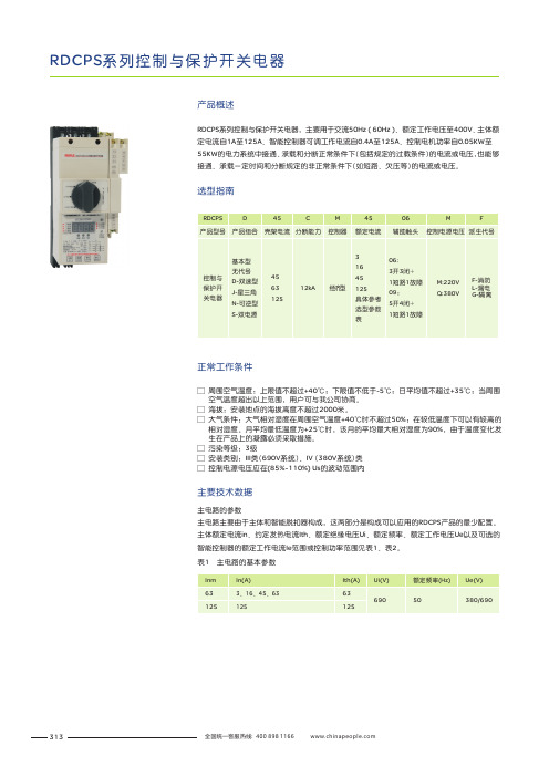
313RDCPS 系列控制与保护开关电器RDCPS 系列控制与保护开关电器,主要用于交流50Hz ( 60Hz )、额定工作电压至400V 、主体额定电流自1A 至125A 、智能控制器可调工作电流自0.4A 至125A 、控制电机功率自0.05KW 至55KW 的电力系统中接通、承载和分断正常条件下(包括规定的过载条件)的电流或电压,也能够接通、承载一定时间和分断规定的非正常条件下(如短路、欠压等)的电流或电压。
□ 周围空气温度:上限值不超过+40℃;下限值不低于-5℃;日平均值不超过+35℃;当周围 空气温度超出以上范围,用户可与我公司协商。
□ 海拔:安装地点的海拔高度不超过2000米。
□ 大气条件:大气相对湿度在周围空气温度+40℃时不超过50%;在较低温度下可以有较高的 相对湿度。
月平均最低温度为+25℃时,该月的平均最大相对湿度为90%,由于温度变化发 生在产品上的凝露必须采取措施。
□ 污染等级:3级□ 安装类别:III 类(690V 系统)、IV (380V 系统)类□ 控制电源电压应在(85%~110%) Us 的波动范围内正常工作条件产品概述选型指南主电路的参数主电路主要由于主体和智能脱扣器构成,这两部分是构成可以应用的RDCPS 产品的最少配置。
主体额定电流in 、约定发热电流Ith 、额定绝缘电压Ui 、额定频率、额定工作电压Ue 以及可选的智能控制器的额定工作电流Ie 范围或控制功率范围见表1、表2。
主要技术数据表1主电路的基本参数314注:□ 瞬时保护参数li 不可调,其值整定在16le电机用产品其短延时保护整定参数ls 可调范围为6lr~12lr □ □ 配电用产品其短延时保护整定参数Is 可调范围为3lr~6lr □ 以上功率范围参考Y 系列三相异步电动机的技术参数 □如有特殊要求时请生产厂家联系表2 主电路的主要参数315RDCPS 系列控制与保护开关电器RDCPS保护特性曲线1.0l r 1最小1.2l r 1最小1.0l r 1最大1.2l r 1最大6l r 1(l r 2最小)12l r 1(l r 2最16l r 1±1520l r 1±20I c s I(A)RDCPS电动机保护时间-电流特性0.1s 0.01s 0.001s1.05l r 1最小1.30l r 1最小1.05l r 1最大1.30l r 1最大3l r 1(l r 2最小)6l r 1(l r 2最大)16l r 1±1520l n ±20%I c sI(A)RDCPS 配电保护时间-电流特性用于电动机控制(使用类别:AC-42、AC-43、AC-44)的动作特性316智能脱扣器主要技术参数□ 起动延时在RDCPS 起动时间内,只对缺相、断相、过压、欠压、欠流、短路、漏电及三相不平衡进行保护,以避免RDCPS 启动大电流和过电流的保护;整定时间为 ( 1~99 ) 秒内之间选择;□ 过压及欠压保护只对辅助电源电压进行保护,以确保线圈与智能控制器正常工作;过压保护:当辅助电源电压超过设定值时(出厂整定在120%Us ),动作时间≤10秒;欠压保护:当辅助电源电压低于设定值时(出厂整定在85%Us ),动作时间≤10秒;□ 反时限过载长延时保护用户根据负载电流I 设定智能脱扣器的额定工作电流Ie ,使负载电流I 在80~100%Ie 之间,动作时间应根据负载特性设定,过流倍数与动作时间特性见表四,反时限过载长延时保护特性曲线出厂设定在F1表3 RDCPS反时限过载长延时保护动作特性用于配电线路负载(使用类别:AC-40、AC-41)的动作特性□ 欠流保护欠流保护:是根据最小电流与额定电流的比值来判断是否启动欠流保护(出厂设定在0),可以对不能空载的电机进行保护;也可以避免用户未根据负载电流I 设定RDCPS 智能脱扣器的工作电流Ie ,从而导致电机不在RDCPS 的保护范围内。
迈普路由器基本配置与维护

显示路由表
? sh ip route
? Codes: C - connected, S - static, R - RIP, O - OSPF, OE-OSPF External, M - Management
?
D - Redirect, E - IRMP, EX - IRMP external, o - SNSP, B - BGP
允许本端
172.168.0.0/24这个网段的地址到任意地址
? interface gigaethernet0
进入相应端口
? ip address 116.52.163.178 255.255.255.248 配置IP地址
? ip nat outside
应用NAT为出方向
? exit
? interface gigaethernet2
? ip dhcp pool 外网
配置DHCP地址池
? network 172.168.0.0 255.255.252.0 配置地址范围
? dns-server 222.172.200.68 61.166.150.123 配置DNS
? default-router 172.168.0.254
? Internet 上 大约99.99%的路由器上都存在一 条缺省路由!
? 缺省路由并不一定都是手工配置的静态路 由,有时也可以由动态路由协议产生。
OSPF路由协议介绍 OSPF协议的一些基本概念
?Router ID
一个32bit 的无符号整数,是一台路由器的唯一标识, 在整个自治系统内唯一。
?协议号
? ip address 172.168.0.254 255.255.252.0
XP151A13A0MR MOS管中文资料
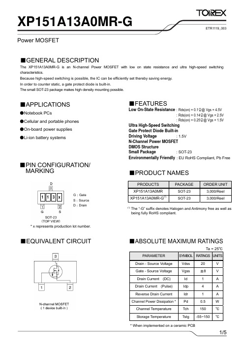
XP151A13A0MR-GPower MOSFETPRODUCTSPACKAGEORDER UNITXP151A13A0MR SOT-23 3,000/Reel XP151A13A0MR-G (*)SOT-233,000/ReelPARAMETER SYMBOL RA TINGS UNITS Drain - Source Voltage Vdss 20VGate - Source Voltage Vgss ±8 V Drain Current (DC) Id 1A Drain Current (Pulse) Idp 4 A Reverse Drain Current Idr1AChannel Power Dissipation * Pd 0.5 W Channel Temperature Tch 150 ℃■GENERAL DESCRIPTIONThe XP151A13A0MR-G is an N-channel Power MOSFET with low on state resistance and ultra high-speed switching characteristics.Because high-speed switching is possible, the IC can be efficiently set thereby saving energy.In order to counter static, a gate protect diode is built-in. The small SOT-23 package makes high density mounting possible.■APPLICATIONS ●Notebook PCs●Cellular and portable phones ●On-board power supplies ●Li-ion battery systems■FEATURESLow On-State Resistance : Rds(on) = 0.1Ω@ Vgs = 4.5V: Rds(on) = 0.14Ω@ Vgs = 2.5V : Rds(on) = 0.25Ω@ Vgs = 1.5V Ultra High-Speed Switching Gate Protect Diode Built-inDriving Voltage : 1.5V N-Channel Power MOSFET DMOS StructureSmall Package : SOT-23Environmentally Friendly : EU RoHS Compliant, Pb Free■PIN CONFIGURATION/ MARKING■PRODUCT NAMES■ABSOLUTE MAXIMUM RATINGS■EQUIVALENT CIRCUITTa = 25℃ETR1119_003G :Gate S :Source D :Drain1 1 3 x* x represents production lot number.(*)The “-G” suffix denotes Halogen and Antimony free as well asbeing fully RoHS compliant.PARAMETER SYMBOL CONDITIONS MIN.TYP .MAX.UNITS Drain Cut-Off Current Idss Vds= 20V, Vgs= 0V - - 10 μA Gate-Source Leak Current Igss Vgs= ±8V, Vds= 0V - - ±10 μA Gate-Source Cut-Off Voltage Vgs(off) Id= 1mA, Vds= 10V 0.5 - 1.2 V Id= 0.5A, Vgs= 4.5V - 0.075 0.100 Ω Id= 0.5A, Vgs= 2.5V - 0.10 0.14 Ω Drain-Source On-State Resistance *1Rds(on)Id= 0.1A, Vgs= 1.5V- 0.17 0.25 Ω Forward Transfer Admittance *1| Yfs | Id= 0.5A, Vds= 10V - 4.2 - S Body Drain Diode Forward VoltageVfIf= 1A, Vgs= 0V-0.81.1VPARAMETER SYMBOL CONDITIONSMIN.TYP .MAX.UNITSThermal Resistance(Channel-Ambience)Rth (ch-a)Implement on a ceramic PCB- 250 - ℃/WPARAMETER SYMBOL CONDITIONSMIN.TYP .MAX.UNITSInput Capacitance Ciss - 220 - pF Output Capacitance Coss - 120 - pF Feedback CapacitanceCrssVds= 10V, Vgs=0Vf= 1MHz - 45 - pFPARAMETER SYMBOL CONDITIONSMIN.TYP .MAX.UNITSTurn-On Delay Timetd (on)- 10 - ns Rise Time tr - 15 - ns Turn-Off Delay Timetd (off) - 75 - nsFall TimetfVgs= 5V, Id= 0.5AVdd= 10V - 65 - ns ■ELECTRICAL CHARACTERISTICSDC CharacteristicsT a = 25℃*1 Effective during pulse test.T a = 25℃Switching CharacteristicsThermal CharacteristicsDynamic CharacteristicsT a = 25℃XP151A13A0MR-G ■TYPICAL PERFOMANCECHARACTERISTICS■TYPICAL PERFOMANCECHARACTERISTICS (Continued)(11) Standardized transition Thermal Resistance vs. Pulse WidthXP151A13A0MR-G。
RD151TS3325ARP中文资料

RD151TS3325ARP中文资料RD151TS3315ARP, RD151TS3325ARP Spread Spectrum Clock for EMI SolutionREJ03D0796-0100Rev.1.00May 11, 2006 DescriptionRD151TS3315ARP and RD151TS3325ARP is a high-performance Spread Spectrum Clock generator. It is suitable for EMI solution of electric systems.FeaturesSupports 20 MHz to 40 MHz operations. Multiple rate (XIN: SSCOUT) = 1: 4Input frequency 80 MHz to 160 MHzSpread spectrum modulation ; RD151TS3315ARP : ±1.5%, ±0.5% (Central spread modulation)RD151TS3325ARP : –3.0%, –1.0% (Down spread modulation) Key SpecificationsSupply voltages: V DD = 3.3 V ±0.3 VCycle to cycle jitter = ±100 ps typ.Clock output duty cycle = 50 ±5%Output slew rate = 0.7 V/ns typ.Ordering InformationPart Name Package TypePackage Code(Previous Code)PackageAbbreviationTaping Abbreviation(Quantity)RD151TS3315ARPH0 RD151TS3325ARPH0 SOP-8 pin (JEDEC)PRSP0008DD-C(FP-8DCV)RP H (2,500 pcs / Reel)Block DiagramPin ArrangementPin DescriptionsPin name No. Type DescriptionpinGNDGND 5Groundpin.supplyPowerVDD 8PowerNC 3 NC Don’t connect any VDD or GND.SSCOUT 6 Output Spread spectrum modulated clock output.input.OscillatorXIN 1InputOscillatoroutput.OutputXOUT 2InputSEL 7SSC% mode select pin. LVCMOS level input.Pull-down by internal resistor (350 k?).InputSSN 4SSC ON/OFF select pin. LVCMOS level input.Pull–down by internal resistor (350 k?).SSC Function TableSTB SEL RD151TS3315ARP(Central spread) RD151TS3325ARP(Down spread)0 0 ±1.5%*1 –3.0%*10 1 ±0.5% –1.0%1 0OFF OFF1 1Note: 1. ±1.5%(TS3315ARP) / -3.0%(TS3325ARP) SSC is selected for default by internal pull-down resistors.Clock Frequency T ableMultiply rate (XIN: SSCOUT)SSCOUT(MHz)PRODUCT XIN(MHz)RD151TS3315ARP 20 to 40 80 to 160 1:4RD151TS3325ARP 20 to 40 80 to 160 1:4Absolute Maximum RatingsItem Symbol Ratings Unit ConditionsSupply voltage V DD –0.5 to 4.6 V Input voltage V I –0.5 to 4.6 VOutput voltage *1V O –0.5 to V DD +0.5 V Input clamp current I IK –50 mA V I < 0 Output clamp current I OK –50 mA V O < 0 Continuous output current I O ±50 mA V O = 0 to V DD Maximum power dissipation 0.7 W T a = 55°C (in still air) Storage temperature T stg –65 to +150 °C Notes: Stresses be yond those listed under “absolute maximum ratings” may cause permanent damage to the device. 1. The input and output negative voltage ratings may be exceeded if the input and output clamp current ratings are observed.Recommended Operating ConditionsItem Symbol Min Typ Max Unit ConditionsSupply voltage V DD 3.0 3.3 3.6 V DC input signal voltage–0.3 — V DD +0.3 VHigh level input voltage V IH 0.7×V DD — V DD +0.3 V Low level input voltage V IL –0.3 —0.3×V DD V Input clock duty cycle 45 50 55 % Operating temperature T a –20 —85 °CDC Electrical CharacteristicsTa = –20 to 85 °C, V DD = 3.0 to 3.6 VItem Symbol Min Typ Max Unit Test Conditions——±20 V I = 0 V or 3.6 V, V DD = 3.6 V,XIN pinInput current I I ——±100 μA V I = 0 V or 3.6 V, V DD = 3.6 V,SEL, SSN pinsInput capacitance C I — 3 — pF SEL, SSN pinsDC Electrical Characteristics / SSC Clock OutputTa = –20 to 85 °C, V DD = 3.0 to 3.6 VItem Symbol Min Typ Max Unit Test Conditions V OH V DD –0.2 —— V I OH = –1 mAOutput voltage V OL —— 200 mV I OL = 1 mAI OH —–44 — V OH = 1.5 V, V DD = 3.3 VOutput current I OL — 44 — mA V OL = 1.5 V, V DD = 3.3 V Output impedance — 40 — ? Note: Parameters are target of design. Not 100% tested in production.AC Electrical Characteristics / SSC Clock OutputT a = 25°C, V DD = 3.3 V, C L = 15 pFItem Symbol Min Typ Max Unit Test Conditions NotesOperating current I DD — 24 30 mA V DD = 3.3 V, C L = 15 pF,XIN = 40 MHzCycle to cycle jitter *1 t CCS — |100| — ps SEL = 0, C L = 0 pF SSC = ±1.5% (TS3315ARP) SSC = –3.0% (TS3325ARP) Figure 1Slew rate t SL — 2.0 5.0 V/ns V DD = 3.3 V,0.2 × V DD to 0.8 × V DDClock duty cycle 45 50 55 %Stabilization time *2—— 2 ms Notes: Parameters are target of design. Not 100% tested in production. 1. Cycle to cycle jitter is included spread spectrum modulation. 2. Stabilization time is the time required for the integrated circuit to obtain phase lock of its input signal afterpower up.Figure 1 Cycle to cycle jitterApplication Information1. Recommended Circuit ConfigurationThe power supply circuit of the optimal performance on the application of a system should refer to Figure 2. VDD decoupling is important to both reduce Jitter and EMI radiation.The C1 decoupling capacitor should be placed as close to the VDD pin as possible, otherwise the increased trace inductance will negate its decoupling capability.Figure 2 Recommended circuit configuration2. Example Board Layout ConfigurationFigure 3 Example Board Layout3. Example of TS33XX EMI Solution IC’s ApplicationFigure 4 Ref. Clock Input ExampleFigure 5 XTAL Ref. Clock Input ExamplePackage Dimensions RENESAS SALES OFFICESRefer to "/en/network" for the latest and detailed information.Renesas Technology America, Inc.450 Holger Way, San Jose, CA 95134-1368, U.S.ATel: <1> (408) 382-7500, Fax: <1> (408) 382-7501Renesas Technology Europe LimitedDukes Meadow, Millboard Road, Bourne End, Buckinghamshire, SL8 5FH, U.K.Tel: <44> (1628) 585-100, Fax: <44> (1628) 585-900Renesas Technology (Shanghai) Co., Ltd.Unit 204, 205, AZIACenter, No.1233 Lujiazui Ring Rd, Pudong District, Shanghai, China 200120Tel: <86> (21) 5877-1818, Fax: <86> (21) 6887-7898Renesas Technology Hong Kong Ltd.7th Floor, North T ower, World Finance Centre, Harbour City, 1 Canton Road, Tsimshatsui, Kowloon, Hong KongTel: <852> 2265-6688, Fax: <852> 2730-6071Renesas Technology Taiwan Co., Ltd.10th Floor, No.99, Fushing North Road, Taipei, TaiwanTel: <886> (2) 2715-2888, Fax: <886> (2) 2713-2999Renesas Technology Singapore Pte. Ltd.1 Harbour Front Avenue, #06-10, Keppel Bay Tower, Singapore 098632Tel: <65> 6213-0200, Fax: <65> 6278-8001Renesas Technology Korea Co., Ltd.Kukje Center Bldg. 18th Fl., 191, 2-ka, Hangang-ro, Yongsan-ku, Seoul 140-702, KoreaTel: <82> (2) 796-3115, Fax: <82> (2) 796-2145Renesas Technology Malaysia Sdn. BhdUnit 906, Block B, Menara Amcorp, Amcorp Trade Centre, No.18, Jalan Persiaran Barat, 46050 Petaling Jaya, Selangor Darul Ehsan, MalaysiaTel: <603> 7955-9390, Fax: <603> 7955-95102006. Renesas Technology Corp., All rights reserved. Printed in Japan.。
莫贾NPort P5150A系列1口RS-232 422 485PoE串行设备服务器产品介绍说明书

NPort P5150A Series1-port RS-232/422/485PoE serial device serversFeatures and Benefits•IEEE802.3af-compliant PoE power device equipment•Speedy3-step web-based configuration•Surge protection for serial,Ethernet,and power•COM port grouping and UDP multicast applications•Screw-type power connectors for secure installation•Real COM and TTY drivers for Windows,Linux,and macOS•Standard TCP/IP interface and versatile TCP and UDP operation modesCertificationsIntroductionNPort®P5150A device servers are designed to make serial devices network-ready in an instant.It is a power device and is IEEE802.3af compliant, so it can be powered by a PoE PSE device without an additional power e the NPort®P5150A device servers to give your PC software direct access to serial devices from anywhere on the network.The NPort®P5150A device servers are ultra-lean,ruggedized,and user-friendly, making simple and reliable serial-to-Ethernet solutions possible.Surge Protection for Serial,Ethernet,and PowerSurge,which is typically caused by high voltages that result from switching and lightning transients,is a common threat to all electrical devices. Moxa’s leading-edge surge immunity solution,which is applied to the NPort®P5150A’s serial,power,and Ethernet lines,is tested and proven compliant with IEC61000-4-5.This state-of-the-art surge protection provides a robust serial-to-Ethernet solution that can protect electrical devices from voltage spikes and withstand electrically noisy environmental conditions.3-Step Web-based ConfigurationThe NPort®P5150A’s3-step web-based configuration tool is straightforward and user-friendly.The NPort®P5150A’s web console guides users through3simple configuration steps that are necessary to activate the serial-to-Ethernet application.With this speedy3-step web-based configuration,a user only needs to spend an average of30seconds to complete the NPort®settings and enable the application,saving a great amount of time and effort.Easy to TroubleshootNPort®P5150A device servers support SNMP,which can be used to monitor all units over Ethernet.Each unit can be configured to send trap messages automatically to the SNMP manager when user-defined errors are encountered.For users who do not use SNMP manager,an email alert can be sent ers can define the trigger for the alerts using Moxa’s Windows utility,or the web console.For example,alerts can be triggered by a warm start,a cold start,or a password change.AppearanceSpecificationsEthernet Interface10/100BaseT(X)Ports(RJ45connector)1Magnetic Isolation Protection 1.5kV(built-in)Standards PoE(IEEE802.3af)Ethernet Software FeaturesConfiguration Options Web Console(HTTP/HTTPS),Windows Utility,Device Search Utility(DSU),TelnetConsole,Serial Console,MCC ToolManagement ARP,BOOTP,DHCP Client,DNS,HTTP,HTTPS,ICMP,IPv4,LLDP,SMTP,SNMPv1/v2c,TCP/IP,Telnet,UDPFilter IGMP v1/v2Windows Real COM Drivers Windows95/98/ME/NT/2000,Windows XP/2003/Vista/2008/7/8/8.1/10(x86/x64),Windows2008R2/2012/2012R2/2016/2019(x64),Windows Embedded CE5.0/6.0,Windows XP EmbeddedLinux Real TTY Drivers Kernel versions:2.4.x,2.6.x,3.x,4.x,and5.xFixed TTY Drivers SCO UNIX,SCO OpenServer,UnixWare7,QNX4.25,QNX6,Solaris10,FreeBSD,AIX5.x,HP-UX11i,Mac OS X,macOS10.12,macOS10.13,macOS10.14,macOS10.15 Android API Android3.1.x and laterMIB RFC1213,RFC1317Serial InterfaceConnector DB9maleNo.of Ports1Serial Standards RS-232,RS-422,RS-485Operation Modes Disabled,Ethernet Modem,Pair Connection,Real COM,Reverse Telnet,RFC2217,TCPClient,TCP Server,UDPBaudrate Supports standard baudrates(unit=bps):50,75,110,134,150,300,600,1200,1800,2400,4800,7200,9600,19200,38400,57600,115200,230.4k,460.8k,921.6kData Bits5,6,7,8Stop Bits1,1.5,2Parity None,Even,Odd,Space,MarkFlow Control RTS/CTS,DTR/DSR,XON/XOFFPull High/Low Resistor for RS-4851kilo-ohm,150kilo-ohmsRS-485Data Direction Control ADDC®(automatic data direction control)Serial SignalsRS-232TxD,RxD,RTS,CTS,DTR,DSR,DCD,GNDRS-422Tx+,Tx-,Rx+,Rx-,GNDRS-485-4w Tx+,Tx-,Rx+,Rx-,GNDRS-485-2w Data+,Data-,GNDPower ParametersInput Current DC Jack I/P:125mA@12VDCPoE I/P:180mA@48VDCInput Voltage12to48VDC(supplied by power adapter),48VDC(supplied by PoE) No.of Power Inputs1Source of Input Power Power input jackPoEReliabilityAutomatic Reboot Trigger Built-in WDTPhysical CharacteristicsHousing MetalDimensions(with ears)100x111x26mm(3.94x4.37x1.02in)Dimensions(without ears)77x111x26mm(3.03x4.37x1.02in)Weight300g(0.66lb)Environmental LimitsOperating Temperature NPort P5150A:0to60°C(32to140°F)NPort P5150A-T:-40to75°C(-40to167°F)Storage Temperature(package included)-40to75°C(-40to167°F)Ambient Relative Humidity5to95%(non-condensing)Standards and CertificationsEMC EN55032/24EMI CISPR32,FCC Part15B Class AEMS IEC61000-4-2ESD:Contact:4kV;Air:8kVIEC61000-4-3RS:80MHz to1GHz:3V/mIEC61000-4-4EFT:Power:2kV;Signal:1kVIEC61000-4-5Surge:Power:2kV;Signal:1kVIEC61000-4-6CS:150kHz to80MHz:3V/m;Signal:3V/mIEC61000-4-8PFMFIEC61000-4-11Safety UL60950-1MTBFTime2,231,530hrsStandards Telcordia(Bellcore)Standard TR/SRWarrantyWarranty Period5yearsDetails See /warrantyPackage ContentsDevice1x NPort P5150A Series device serverDocumentation1x quick installation guide1x warranty cardDimensionsOrdering InformationModel Name Operating Temp.Baudrate Serial Standards No.of Serial Ports Input VoltageNPort P5150A0to60°C50bps to921.6kbps RS-232/422/485112-48VDC by power adapter or48VDC by PoENPort P5150A-T-40to75°C50bps to921.6kbps RS-232/422/485112-48VDC by power adapter or48VDC by PoEAccessories(sold separately)CablesCBL-F9M9-150DB9female to DB9male serial cable,1.5mCBL-F9M9-20DB9female to DB9male serial cable,20cmConnectorsADP-RJ458P-DB9F DB9female to RJ45connectorMini DB9F-to-TB DB9female to terminal block connectorDIN-Rail Mounting KitsDK35A DIN-rail mounting kit,35mmPower AdaptersPWR-12050-USJP-S2PWR-12050-USJP-S2PWR-12050-EU-S2PWR-12050-EU-S2PWR-12050-CN-S2PWR-12050-CN-S2PWR-12050-UK-S2PWR-12050-UK-S2PWR-12050-AU-S2PWR-12050-AU-S2PWR-12150-AU-SA-T Locking barrel plug,12VDC,1.5A,100to240VAC,Australia(AU)plug,-40to75°C operatingtemperaturePWR-12150-CN-SA-T Locking barrel plug,12VDC,1.5A,100to240VAC,China(CN)plug,-40to75°C operatingtemperaturePWR-12150-EU-SA-T Locking barrel plug,12VDC,1.5A,100to240VAC,Continental Europe(EU)plug,-40to75°Coperating temperaturePWR-12150-UK-SA-T Locking barrel plug,12VDC,1.5A,100to240VAC,United Kingdom(UK)plug,-40to75°C operatingtemperaturePWR-12150-USJP-SA-T Locking barrel plug,12VDC1.5A,100to240VAC,United States/Japan(US/JP)plug,-40to75°Coperating temperaturePWR-Plug-USJP-02PWR-Plug-USJP-02PWR-Plug-EU-02PWR-Plug-EU-02PWR-Plug-CN-02PWR-Plug-CN-02PWR-Plug-UK-02PWR-Plug-UK-02PWR-Plug-AU-02PWR-Plug-AU-02Power CordsCBL-PJ21NOPEN-BK-30Locking barrel plug to bare-wire cable©Moxa Inc.All rights reserved.Updated Jun23,2021.This document and any portion thereof may not be reproduced or used in any manner whatsoever without the express written permission of Moxa Inc.Product specifications subject to change without notice.Visit our website for the most up-to-date product information.。
180个电视机CPU主要引脚功能表_元件参数_家电配件网手机版

180个电视机CPU主要引脚功能表_元件参数_家电配件网手机版日期:2013-03-08 09:39微处理器型号应用彩电型号待机控制电源电压时钟振荡复位端音量控制M491 熊猫3608A 26 9 7、8 9 15 M494B1 飞跃54C2Y-2 38 39 25、26 34 M37100M8-581 东芝329P8M 25 1 28、29 27 2 M37102M8 牡丹64C2 58 64 30、31 29 55 M50124SA M50162SA 三洋CTP-6925-00 10 21 2、3 23 41 M50161-554SP 日立CTP-2005D 23 24、25 26 19 M50163-150SP 日立CTP-2008SP 31 21 2、3 23 41 M50430-581SP 东芝182E5C 1 9、10 6 27 M50431-101SP 长城JTC-512 27 42 1、2 36 28 M50431-513SP 索尼KV-2182CH 27 42 1、2 36 28 M50432-551SP 日立CPT-2157SF 30 42 33 34 16 14 M50433-531SP 双喜C541PD-1 16 1 33 34 11 27 M50435-893FP JVC-210C 14 1 33 34 11 27 M50453-101SP 佳丽彩EC-2063R 27 42 1、2 36 28 M50436-560SP 熊猫3631 9 52 28 29 27 2 M50436-582SP 东芝288D6C 6 52 28 29 27M50436-683SP 东芝2500XH 6 52 28 29 27 3 M50436-585SP M50436-589SP东芝289X6M2 6 52 28 29 27 4 M50436-688SP 东芝248X9M 6 52 28 29 27 3 M50436-602SP 牡丹51C5 10 52 28 29 27 2 M34300N4-011SP 快乐HC2808R 30 42 34 35 7 10 M34300N4-012SP 夏华XT-7698T 30 42 34 35 7 10 M34300N4-551SP 日立G7-X 1 42 34 35 7 10 M34300N4-657SP 日立CMT-2518 1 42 34 35 7 10 M37103M4-655SP 日立C21D8A 42 1 28 29 27 2 M34300N4-555SP 日立CMT-2518 30 42 34 35 7 10 M34300N4-584SP 华日C54J-1 33 42 34 35 7 13 M34300N4-585SP 东芝206Q9M 33 42 34 35 7 13 M34300N4-587SP 东芝219R9C 33 42 34 35 7 13 M34300N4-624SP 北京2132MA 17 42 34 35 7 10 M34300N4-628SP 长虹C2151A 17 42 34 35 7 10 M34300N4-721SP 海信TC2520 17 42 34 35 7 10 M37210M3-508SP 熊猫2128 21 27 24 25 30 3 M37210M3-800SP 康佳T2588B 21 27 24 25 30 3 M37210M3-902SP 康佳T3877N 21 27 24 25 30 3 M37210M4-650SP 日立CMT2579-041 27 24 25 30 8M37210M4-688SP熊猫2518 31 27 24 25 30M37210M4-786SPM37210M4-705SP 康佳T3477N 21 27 24 25 30 3M37211M2-609SP 康佳T2989H 22 27 24 25 30 3M37222M6-B80SP 东芝2150XH 7 42 31 32 33M34302MB-612SP 索尼KV-2189TC 6 52 28 29 27 2M37210M3-010SP 康力CE-6448-1 21 27 24 25 30 3M37204MB-852SP 日立CMT2598 58 64 30 31 29M37103M4-750SP 福日HFC-2168 42 1 28 29 27 2M37102M8-503SP 福日HFC-2587 58 64 30 31 29 7M37102M8-509SP 乐华MC-15A 44 64 30 31 29M37220M3 康佳T2136F 26 22 19 20 25 34 MN15151TWE MN15151TWP 松下C-150 29 1 44 45 7 16 MN1871611TKA 松下TC-V292H 6 22 62 63 54 45 MN1872432TWI 松下TC-29V30R 33 22 61 62 63 54 45 MN1874033TNW 松下三超画王33 22 61 62 63 54 24 MN152810TTC3 松下TC-21L3RQ 29 1 44 45 7 16 MN152811TZX 松下TC-2150R 24 1 35 36 7 16 MN1871675T6S 松下TC-29GF70R 35 22 62 63 54MN1871274 长虹R2519N 39 40 41 34MN15245KWC MN15245SAY 华强69510-00 21 42 40 41 8 34 MN14821JTB MN14821TKG 龙江7755JM 7 1 18 19 2 22 MN15142TEAI 松下TC-2185 6 39 37 38 8 32 MN15282 MN15287 康佳2916A 8 52 2、3 4 44 TMP47C433AN 牡丹54C10 8 42 31 32 33 2 TMP47C430N 熊猫C44P3 27 28 22 23 21 2 TMP47C434N 康佳T914H 22 42 31 32 33 2 TMP47C837N 熊猫2158 22 42 31 32 33 4 TMP43238135A 黄河HC47-3 14 42 24 25 23 20 TMP47C1638AU353 长虹C2919P 31 54 42 43 44 2 TMP47C634AN 快乐HC2983N 22 42 31 32 33 2 TMP47C1238ANU068 长虹C2588P 10 54 42 43 44TMP87PM36N 康佳T3888 34 42 31 32 33 2 TMP73C47 长城G8135BF 15 1 33 34 32 39 TMP87CM38N 长虹T2981 7 42 31 32 33TMP87CH33N 19 42 31 32 33 1 TMP47C834N-R122 东芝2125XH 8 42 31 32 33 5 TC9150P 康佳KTN-5145 10 24 22 23 5、6 TC9002AP 东芝C-2021Z 10 3、4TD6368B4/FHO 康佳T2979D1 37 42 31 32 33 5 HD44840A65 汤姆逊TFE5114DK 7 21 17 18 15 13 GS8234-01F 牡丹64C1 44 64 30 31 29LK5103 长城JTC-531 8 42 31 32 33 2LK5140 22 42 31 32 33 2KD9218B 北京8356C 7 23 31 32 24 1 KY88C94 厦华XT7688T 61 15 49 50 55 51 KAIDA8803A 北京8306-3Y 40 1 2、3 6 34 UPD1514C-036 日立N982 1 28 15 16 17 22 UPD1937C 51CD5 1 12 10、11 7 Z86227 牡丹CW25638 4 14 7 、8 9 37 Z86227-SR1285 金星C5416 32 14 7、8 9 40 Z90103-JX-2 金星C5417 32 14 7、8 9 40 Z90361 康佳T3289W 38 34 31 32 33BM5069 松下TC-M25C 32 52 28 29 27 1 CKP1003S 康佳P2993N 24 42 31 32 33 2 CKP1008S 康佳2592N 20 42 31 32 33CKP1009S 康佳A2109E 20 42 31 32 33CKP1105S 康佳F2109C 35 34 31 32 33 6 CKP1301S 康佳F2109E2 20 42 31 32 33CH4001-5B41 长虹C2155 8 13 40 11、12 16 36 CH04001-5553 长虹C2151C 8 13 40 11、12 16 36 CH04001-5C25 长虹C1951K 8 13 40 11、12 16 36 CH0403-5H61 长虹A2928B 7 12、21 10、11 17 39 CH04801-5F43 长虹P2119A 7 12、21 10、11 17 39 CH05001 长虹C2995 41 42 31 32 33 2 CTV222S.PRC1 康佳T2516 41 42 31 32 33 2CTV591S.GW3 海尔692-733AM-0241 42 31 32 33CXP80424-146 东芝3429KTP 37 64 34 35 36 CXP85332-108 东芝 F3SS 机芯37 63 64 34 35 36LA86C3348A 创维 Y 机芯7 12 10、11 17LC863320A 康佳F2979A 7 12 10、11 17 5 LC863324 TCL王牌-2116E 7 12 10、11 17 8 LC863328A-5T45 康佳T2188A 7 12 10、11 17 5 LC863348A 康佳F2109A 7 12 10、11 17 5LC864012L-5711 环宇新宇宙王C5420BZ8 13 11、12 16 36LC864512V-5D18 海尔HS-2588D 7 12、21 10、11 17MN181768 创维 5N10 机芯21 29 40 41 34 14 MN1874876TSH 松下TC-33GF85 33 22 62 63 54 16 TMS73C167 海尔H-2916 10 54 43 44 45 4 TMP47C834N-R122 东芝2128KTV 8 42 31 32 33TMP87CH36N 厦华XT3868T 34 42 31 32 33 2 TMP87CM36N-3649 厦华XT29F8THD 34 42 31 32 33 2 TMP87CK36N 康佳T2988P 34 42 31 32 33 2 TMP87CX38N 康佳T2166E 20 42 31 32 33TMP87CP38N 长虹G2967A 7 42 31 32 33TMP87CH38N 厦华XT-3465 7 42 31 32 33TMP87PS38N 海信TC2902GD 7 42 31 32 33TMP87CK38N TCL王牌2901A 18 42 31 32 33 4 TMP87CS38N 飞利蒲29H8 8 42 31 32 33 6ST6368B4/FHO 康佳T2979D1 37 42 31 32 33 5ST6388 创维 5S01 机芯37 5 31 32 33P87C770 飞利蒲29G8 19 38 39 41 42 43P83C266BDR 海信TC2532F 3、41 28 30 31 32 33 12 ONWA KWEC 康佳T2510 8 52 2、 3 4 44 WH2000C 海尔HP-3408 41 34 31 32 33KONKA266 康佳P3486C 14 28 31 32 33 2KS88C8324 长虹G2573 42 34 31 32 33Z8933212PSC 北京2163 18 34 31 32 33Z90231 康佳F2109C 35 34 31 32 33 6 CCU-2070-LDTV-06A 福日HFC2553 28 27 1 4CH05002 长虹D2963A 41 42 31 32 33 2 CHT0406 长虹R2118K 7 12 10、11 17CHT0803 长虹43PT18 41 42 31 32 33CHT0807 长虹2131FB 7 42 31 32 33CHT0808 长虹29SD83 41 42 31 32 33CKP1001S 康佳T2133G 17 34 31 32 33 2 CKP1004S 康佳T2139N 20 42 31 32 33 2 CKP1101S 康佳T2990N 38 34 31 32 33CKP1103S 康佳T2992N 38 34 28 29 33CTV222S.PRC1 康佳T2516 41 42 31 32 33 2CX519004P 索尼KV-2062CH 10 21 2、3 23 41 CX85116B-621S 索尼KV-2168MT 64 34 35 36CX513-512P 索尼KV-2090CH 1 9、10 6CX522-054 索尼KV-1882CH 2 41 22 23 24CX523-110P 索尼KV-2062CH 17 21 2、3 36 41 CXP80420-134S 金星C7428 37 64 34 35 36CXP80420-139S 北京3931H 37 64 34 35 36 5、6 CXP80424-165S 东芝2929KTP-Ⅱ37 64 34 35 36 9、10 CXP85332-512 东芝F3SS机芯37 34 35 36PCA84C440/401 TCL-9329SP 41 42 31 32 33 2 PCA84C640/019 金星C498 41 42 31 32 33 2 PCA84C841/177 长虹D2965 41 42 31 32 33 2PCF84C644 飞利蒲21GX3566193S19 42 31 32 33 2P87C766 康佳T3498 41 42 31 32 33IX0237CE 夏普C-1885DK 20 14 12、13 4 17 IX0411CEN 夏普DV-5406 15 21 2、3 23 41 IX0442CE 夏普C-5405DK 14 30 24 25 26 19 IX0605CE 夏普C-1805DK 1 9、10 6IX0933CE 夏普CV-2121DK 16 1 33 34 11 27IX0981CE 夏普29S21-A1 7 42 40 41 1 36 IX1194CE 夏普8P-MW2 7 42 40 41 1 36 IX1830CE 夏普CV-2189 58 64 30 31 29 7 IX2321CE 夏普21D-CM 32 27 24 25 30 8 IX2372CE 夏普W328 46 64 30 31 29IX2504CE 夏普21FN1 22 27 24 25 30LC863316A 康佳F2109A 7 12 10、11 17 5 LC864512A-5C77 海信TC2139 7 12 10、11 17 39 LC864516AN 海信TC2146 7 12 10、11 17 39 LC864525A 长虹A2928B 7 12 10、11 17 39 LC864916A 康佳F2589D 7 12 10、11 16 26 SAA1293 上海Z247-8A 5 2 1、6 4 34 SC430402CFC 长虹43PT18 14 57 59 71ST63156 福日2108H 2 40 25 26 24 39 ST6367B1/FEJ 康佳T5432E 37 42 31 32 33 5 ST6378B4/FR1 康佳F2977D2 37 42 31 32 33 5。
电源开关管参数文档
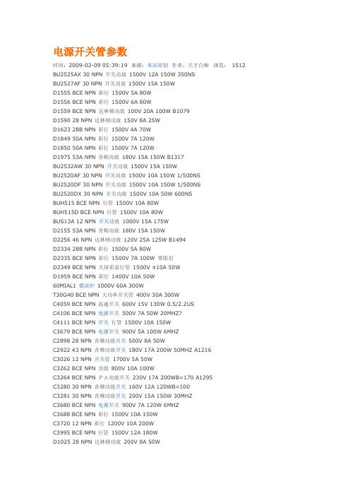
电源开关管参数时间:2009-02-09 05:39:19 来源:本站原创作者:天才白痴浏览:1512BU2525AX 30 NPN 开关功放1500V 12A 150W 350NSBU2527AF 30 NPN 开关功放1500V 15A 150WD1555 BCE NPN 彩行1500V 5A 80WD1556 BCE NPN 彩行1500V 6A 80WD1559 BCE NPN 达林顿功放100V 20A 100W B1079D1590 28 NPN 达林顿功放150V 8A 25WD1623 28B NPN 彩行1500V 4A 70WD1849 50A NPN 彩行1500V 7A 120WD1850 50A NPN 彩行1500V 7A 120WD1975 53A NPN 音频功放180V 15A 150W B1317BU2532AW 30 NPN 开关功放1500V 15A 150WBU2520AF 30 NPN 开关功放1500V 10A 150W 1/500NSBU2520DF 30 NPN 开关功放1500V 10A 150W 1/500NSBU2520DX 30 NPN 开关功放1500V 10A 50W 600NSBUH515 BCE NPN 行管1500V 10A 80WBUH515D BCE NPN 行管1500V 10A 80WBUS13A 12 NPN 开关功放1000V 15A 175WD2155 53A NPN 音频功放180V 15A 150WD2256 46 NPN 达林顿功放120V 25A 125W B1494D2334 28B NPN 彩行1500V 5A 80WD2335 BCE NPN 彩行1500V 7A 100W 带阻尼D2349 BCE NPN 大屏彩显行管1500V ±10A 50WD1959 BCE NPN 彩行1400V 10A 50W60MIAL1 微波炉1000V 60A 300WT30G40 BCE NPN 大功率开关管400V 30A 300WC4059 BCE NPN 高速开关600V 15V 130W 0.5/2.2USC4106 BCE NPN 电源开关500V 7A 50W 20MHZ?C4111 BCE NPN 开关行管1500V 10A 150WC3679 BCE NPN 电源开关900V 5A 100W 6MHZC2898 28 NPN 音频功放开关500V 8A 50WC2922 43 NPN 音频功放开关180V 17A 200W 50MHZ A1216C3026 12 NPN 开关管1700V 5A 50WC3262 BCE NPN 功放800V 10A 100WC3264 BCE NPN PA功放开关230V 17A 200WB=170 A1295C3280 30 NPN 音频功放开关160V 12A 120WB=100C3281 30 NPN 音频功放开关200V 15A 150W 30MHZC3680 BCE NPN 电源开关900V 7A 120W 6MHZC3688 BCE NPN 彩行1500V 10A 150WC3720 12 NPN 彩行1200V 10A 200WC3995 BCE NPN 行管1500V 12A 180WD1025 28 NPN 达林顿功放200V 8A 50WC3997 BCE NPN 行管1500V 15A 250WC3998 BCE NPN 行管1500V 25A 250WC4024 BCE NPN 功放开关100V 10A 35W 24MHZD1037 BCE NPN 音频功放开关150V 30A 180WD1047 30 NPN 音频功放开关160V 12A 100W B817C4119 BCE NPN 微波炉开关1500V 15A 250WC4237 BCE NPN 高压高速开关1000V 8A 120W 30MHZ C4242 BCE NPN 高压高速开关450V 7A 40WC4297 BCE NPN 电源开关500V 12A 75W 10MHZC4429 BCE NPN 电源开关1100V 8A 60WC4532 BCE NPN 大屏行管1700V 10A 200WC4582 BCE NPN 电源开关600V 15A 75W 20MHZC5244 BCE NPN 彩行1700V 15A 200WC5250 BCE NPN 开关1000V 7A 100WC5251 BCE NPN 彩行1500V 12A 50WD1071 28 NPN 达林顿功放300V 6A 40WC4706 BCE NPN 电源开关900V 14A 130W 6MHZC4742 46 NPN 彩行1500V 6A 50WC4745 46 NPN 彩行1500V 6A 50WC4747 46 NPN 彩行1500V 10A 50WC4769 BCE NPN 微机行管1500V 7A 60WC4927 BCE NPN 行管1500V 8A 50WC4927 BCE NPN SONY29行管1500V 8A 50WC4941 BCE NPN 行管1500V 6A 65W 500/380NSC5020 BCE NPN 彩行1000V 7A 100WC5068 BCE NPN 彩行1500V 10A 50WC5086 BCE NPN 彩行1500V 10A 50WC5088 BCE NPN 彩行1500V 10A 50WC5129 BCE NPN 彩显行管1500V 8A 50WD1163A 28 NPN 行偏转用350V 7A 40W 60MHZD1175 12 NPN 行偏转用1500V 5A 100WC5132 BCE NPN 彩行1500V 16A 50WC5144 BCE NPN 大屏彩行1700V 20A 200WC5148 BCE NPN 大屏彩行1500V 8A 50WC5149 BCE NPN 高速高频行管1500V 8A 50WC5198 BCE NPN 功放开关140V 10A 100WC5200 BCE NPN 功放开关230V 15A 150W A1943C5207 BCE NPN 彩行1500V 10A 50WC5243 BCE NPN 彩行1700V 15A 200WC5252 BCE NPN 彩行1500V 15A 100WC5294 BCE NPN 彩行1500V 20A t=200MSC5296 BCE NPN 开关管带阻1500V 8A 80WC5297 BCE NPN 开关管1500V 16A 60WC5331 BCE NPN 大屏彩显行管1500V 15A 180W D325 BCE NPN 功放开关50V 3A 25WD385 11 NPN 达林顿功放100V 7A 30WD1398 BCE NPN 开关1500V 5A 50W 3MHZD1403 BCE NPN 彩行1500V 6A 120W。
- 1、下载文档前请自行甄别文档内容的完整性,平台不提供额外的编辑、内容补充、找答案等附加服务。
- 2、"仅部分预览"的文档,不可在线预览部分如存在完整性等问题,可反馈申请退款(可完整预览的文档不适用该条件!)。
- 3、如文档侵犯您的权益,请联系客服反馈,我们会尽快为您处理(人工客服工作时间:9:00-18:30)。
RD151TS3314ARP, RD151TS3324ARP Spread Spectrum Clock for EMI SolutionREJ03D0795-0100Rev.1.00May 11, 2006 DescriptionRD151TS3314ARP and RD151TS3324ARP is a high-performance Spread Spectrum Clock generator. It is suitable for EMI solution of electric systems.Features• Supports 20 MHz to 40 MHz operations. Multiple rate (XIN: SSCOUT) = 1: 2Input frequency 40 MHz to 80 MHz• Spread spectrum modulation ; RD151TS3314ARP : ±1.5%, ±0.5% (Central spread modulation)RD151TS3324ARP : -3.0%, -1.0% (Down spread modulation)Key Specifications• Supply voltages: V DD = 3.3 V ±0.3 V• Cycle to cycle jitter = ±100 ps typ.• Clock output duty cycle = 50 ±5%• Output slew rate = 0.7 V/ns typ.• Ordering InformationPart Name Package TypePackage Code(Previous Code)PackageAbbreviationTaping Abbreviation(Quantity)RD151TS3314ARPH0 RD151TS3324ARPH0 SOP-8 pin(JEDEC)PRSP0008DD-C(FP-8DCV)RP H (2,500 pcs / Reel)Block DiagramPin ArrangementPin DescriptionsPin name No. Type DescriptionpinGNDGND 5Groundpin.supplyPowerVDD 8PowerNC 3 NC Don’t connect any VDD or GND.SSCOUT 6 Output Spread spectrum modulated clock output.input.OscillatorXIN 1InputOscillatoroutput.OutputXOUT 2InputSEL 7SSC% mode select pin. LVCMOS level input.Pull-down by internal resistor (350 kΩ).InputSSN 4SSC ON/OFF select pin. LVCMOS level input.Pull–down by internal resistor (350 kΩ).SSC Function TableSTB SEL RD151TS3314ARP(Central spread) RD151TS3324ARP(Down spread)0 0 ±1.5%*1 –3.0%*10 1 ±0.5% –1.0%1 0OFF OFF1 1Note: 1. ±1.5%(TS3314ARP) / -3.0%(TS3324ARP) SSC is selected for default by internal pull-down resistors.Clock Frequency TableMultiply rate (XIN: SSCOUT)SSCOUT(MHz)PRODUCT XIN(MHz)RD151TS3314ARP 20 to 40 40 to 80 1:2RD151TS3324ARP 20 to 40 40 to 80 1:2Absolute Maximum RatingsItem Symbol Ratings Unit ConditionsSupply voltage V DD –0.5 to 4.6 V Input voltage V I –0.5 to 4.6 VOutput voltage *1V O –0.5 to V DD +0.5 V Input clamp current I IK –50 mA V I < 0 Output clamp current I OK –50 mA V O < 0 Continuous output current I O ±50 mA V O = 0 to V DD Maximum power dissipation 0.7 W Ta = 55°C (in still air) Storage temperature T stg –65 to +150 °C Notes: Stresses beyond those listed under “absolute maximum ratings” may cause permanent damage to the device. 1. The input and output negative voltage ratings may be exceeded if the input and output clamp current ratingsare observed.Recommended Operating ConditionsItem Symbol Min Typ Max Unit ConditionsSupply voltage V DD 3.0 3.3 3.6 V DC input signal voltage–0.3 — V DD +0.3 VHigh level input voltage V IH 0.7×V DD — V DD +0.3 V Low level input voltage V IL –0.3 — 0.3×V DD V Input clock duty cycle 45 50 55 % Operating temperature –20 — 85 °CDC Electrical CharacteristicsTa = –20 to 85 °C, V DD = 3.0 to 3.6 VItem Symbol Min Typ Max Unit Test Conditions— — ±20 V I = 0 V or 3.6 V, V DD = 3.6 V,XIN pinInput current I I — — ±100 µA V I = 0 V or 3.6 V, V DD = 3.6 V,SEL, SSN pinsInput capacitance C I — 3 — pF SEL, SSN pinsDC Electrical Characteristics / SSC Clock OutputTa = –20 to 85 °C, V DD = 3.0 to 3.6 VItem Symbol Min Typ Max Unit Test Conditions V OH V DD -0.2 — — V I OH = –1 mAOutput voltage V OL — — 200 mV I OL = 1 mAI OH — –19 — V OH = 1.5 V, V DD = 3.3 VOutput current I OL — 19 — mA V OL = 1.5 V, V DD = 3.3 VOutput impedance — 40 — Ω Notes: Parameters are target of design. Not 100% tested in production.AC Electrical Characteristics / SSC Clock OutputTa = 25°C, V DD = 3.3 V, C L = 15 pFItem Symbol Min Typ Max Unit Test Conditions NotesOperating current I DD — 16 22 mA V DD = 3.3 V, C L = 15 pF,XIN = 40 MHzCycle to cycle jitter *1 t CCS — |100| — ps SEL = 0, C L = 0 pF SSC = ±1.5% (TS3314ARP) SSC = –3.0% (TS3324ARP)Figure 1Slew rate t SL — 0.8 4.0 V/ns V DD = 3.3 V,0.2 × V DD to 0.8 × V DDClock duty cycle 45 50 55 % Stabilization time *2 — — 2 ms Notes: Parameters are target of design. Not 100% tested in production. 1. Cycle to cycle jitter is included spread spectrum modulation. 2. Stabilization time is the time required for the integrated circuit to obtain phase lock of its input signal afterpower up.Figure 1 Cycle to cycle jitterApplication Information1. Recommended Circuit ConfigurationThe power supply circuit of the optimal performance on the application of a system should refer to Figure 2. VDD decoupling is important to both reduce Jitter and EMI radiation.The C1 decoupling capacitor should be placed as close to the VDD pin as possible, otherwise the increased trace inductance will negate its decoupling capability.Figure 2 Recommended circuit configuration2. Example Board Layout ConfigurationFigure 3 Example Board Layout3. Example of TS33XX EMI Solution IC’s ApplicationFigure 4 Ref. Clock Input ExampleFigure 5 XTAL Ref. Clock Input ExamplePackage Dimensions RENESAS SALES OFFICESRefer to "/en/network" for the latest and detailed information.Renesas Technology America, Inc.450 Holger Way, San Jose, CA 95134-1368, U.S.ATel: <1> (408) 382-7500, Fax: <1> (408) 382-7501Renesas Technology Europe LimitedDukes Meadow, Millboard Road, Bourne End, Buckinghamshire, SL8 5FH, U.K.Tel: <44> (1628) 585-100, Fax: <44> (1628) 585-900Renesas Technology (Shanghai) Co., Ltd.Unit 204, 205, AZIACenter, No.1233 Lujiazui Ring Rd, Pudong District, Shanghai, China 200120Tel: <86> (21) 5877-1818, Fax: <86> (21) 6887-7898Renesas Technology Hong Kong Ltd.7th Floor, North Tower, World Finance Centre, Harbour City, 1 Canton Road, Tsimshatsui, Kowloon, Hong KongTel: <852> 2265-6688, Fax: <852> 2730-6071Renesas Technology Taiwan Co., Ltd.10th Floor, No.99, Fushing North Road, Taipei, TaiwanTel: <886> (2) 2715-2888, Fax: <886> (2) 2713-2999Renesas Technology Singapore Pte. Ltd.1 Harbour Front Avenue, #06-10, Keppel Bay Tower, Singapore 098632Tel: <65> 6213-0200, Fax: <65> 6278-8001Renesas Technology Korea Co., Ltd.Kukje Center Bldg. 18th Fl., 191, 2-ka, Hangang-ro, Yongsan-ku, Seoul 140-702, KoreaTel: <82> (2) 796-3115, Fax: <82> (2) 796-2145Renesas Technology Malaysia Sdn. BhdUnit 906, Block B, Menara Amcorp, Amcorp Trade Centre, No.18, Jalan Persiaran Barat, 46050 Petaling Jaya, Selangor Darul Ehsan, MalaysiaTel: <603> 7955-9390, Fax: <603> 7955-9510© 2006. Renesas Technology Corp., All rights reserved. Printed in Japan.。