FQT13N06L中文资料
FQP13N50C中文资料
--
--
IGSSF IGSSR
Gate-Body Leakage Current, Forward VGS = 30 V, VDS = 0 V Gate-Body Leakage Current, Reverse VGS = -30 V, VDS = 0 V
--
--
--
--
--
--
1 10 100 -100
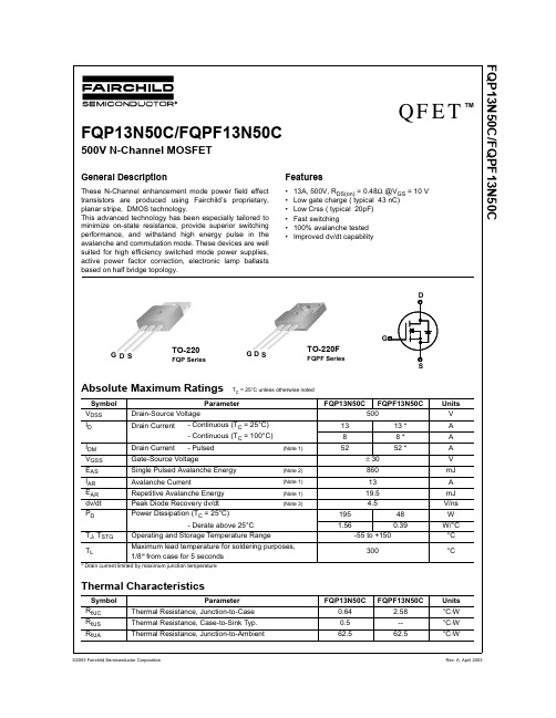
FQP13N50C FQPF13N50C
500
13
13 *
8
8*
52
52 *
± 30
860
13
19.5
4.5
195
48
1.56
0.39
-55 to +150
300
Units V A A A V mJ A mJ
V/ns W
W/°C °C
°C
Thermal Characteristics
Symbol RθJC RθJS RθJA
2.0 --
4.0
V
VGS = 10 V, ID = 6.5 A
-- 0.39 0.48
Ω
VDS = 40 V, ID = 6.5 A
(Note 4) --
15
--
S
Dynamic Characteristics
Ciss
Input Capacitance
Coss
Output Capacitance
Crss
Drain Current - Continuous (TC = 25°C)
- Continuous (TC = 100°C)
IDM
Drain Current - Pulsed
FQAF85N06中文资料

Figure 5. Capacitance Characteristics
VGS , Gate-Source Voltage [V]
IDR, Reverse Drain Current [A]
ID, Drain Current [A]
102
101 175℃
25℃ -55℃
※ Notes :
1. 2.
-55 to +175
300
Thermal Characteristics
Symbol RθJC RθJA
Parameter Thermal Resistance, Junction-to-Case Thermal Resistance, Junction-to-Ambient
Typ
Max
--
1.5
4
2
※ Note : I = 85A D
0
0
20
40
60
80
100
QG, Total Gate Charge [nC]
Figure 6. Gate Charge Characteristics
Capacitance [pF]
©2001 Fairchild Semiconductor Corporation
--
40
Units V A A A V mJ A mJ
V/ns W
W/°C °C
°C
Units °C/W °C/W
©2001 Fairchild Semiconductor Corporation
Rev. A1. May 2001
FQAF85N06
元器件交易网
Electrical Characteristics
FAIRCHILD FQT13N06 说明书

现货库存、技术资料、百科信息、热点资讯,精彩尽在鼎好!FQT13N06Absolute Maximum Ratings T C= 25°C unless otherwise notedParameterDrain-Source VoltageDrain Current- Continuous (T C = 25°C)- Continuous (T C = 70°C)Drain Current- PulsedGate-Source VoltageSOT-223FQT SeriesGDSNotes:1. Repetitive Rating : Pulse width limited by maximum junction temperature2. L = 12.6mH, I AS = 2.8A, V DD = 25V, R G = 25 Ω, Starting T J = 25°C3. I SD ≤ 13A, di/dt ≤ 300A/us, V DD ≤ BV DSS, Starting T J = 25°C4. Pulse Test : Pulse width ≤300µs, Duty cycle ≤2%5. Essentially independent of operating temperatureDSS GS D ∆BV DSS / ∆T J Breakdown Voltage Temperature CoefficientI D = 250 µA, Referenced to 25°C--0.06--V/°C I DSS Zero Gate Voltage Drain Current V DS = 60 V, V GS = 0 V ----1µA V DS = 48 V, T C = 150°C ----10µA I GSSF Gate-Body Leakage Current, Forward V GS = 25 V, V DS = 0 V ----100nA I GSSRGate-Body Leakage Current, ReverseV GS = -25 V, V DS = 0 V-----100nAOn CharacteristicsV GS(th)Gate Threshold VoltageV DS = V GS , I D = 250 µA 2.0-- 4.0V R DS(on)Static Drain-Source On-Resistance V GS = 10 V, I D = 1.4 A --0.110.14Ωg FSForward TransconductanceV DS = 25 V, I D = 1.4 A--3.0--SDynamic CharacteristicsC iss Input Capacitance V DS = 25 V, V GS = 0 V, f = 1.0 MHz--240310pF C oss Output Capacitance--90120pF C rssReverse Transfer Capacitance--1520pFSwitching Characteristicst d(on)Turn-On Delay Time V DD = 30 V, I D = 6.5 A,R G = 25 Ω--520ns t r Turn-On Rise Time --2560ns t d(off)Turn-Off Delay Time --825ns t f Turn-Off Fall Time --1540ns Q g Total Gate Charge V DS = 48 V, I D = 13 A,V GS = 10 V-- 5.87.5nC Q gs Gate-Source Charge -- 2.0--nC Q gdGate-Drain Charge--2.5--nCDrain-Source Diode Characteristics and Maximum RatingsI S Maximum Continuous Drain-Source Diode Forward Current ---- 2.8A I SM Maximum Pulsed Drain-Source Diode Forward Current----11.2A V SD Drain-Source Diode Forward Voltage V GS = 0 V, I S = 2.8 A ---- 1.5V t rr Reverse Recovery Time V GS = 0 V, I S = 13 A,dI F / dt = 100 A/µs --39--ns Q rrReverse Recovery Charge--40--nC(Note 4)(Note 4, 5)(Note 4, 5)(Note 4)DISCLAIMERFAIRCHILD SEMICONDUCTOR RESERVES THE RIGHT TO MAKE CHANGES WITHOUT FURTHER NOTICE TO ANY PRODUCTS HEREIN TO IMPROVE RELIABILITY, FUNCTION OR DESIGN. FAIRCHILD DOES NOT ASSUME ANY LIABILITY ARISING OUT OF THE APPLICATION OR USE OF ANY PRODUCT OR CIRCUIT DESCRIBED HEREIN;NEITHER DOES IT CONVEY ANY LICENSE UNDER ITS PATENT RIGHTS, NOR THE RIGHTS OF OTHERS.LIFE SUPPORT POLICYFAIRCHILD’S PRODUCTS ARE NOT AUTHORIZED FOR USE AS CRITICAL COMPONENTS IN LIFE SUPPORT DEVICES OR SYSTEMS WITHOUT THE EXPRESS WRITTEN APPROVAL OF FAIRCHILD SEMICONDUCTOR CORPORATION.As used herein:1. Life support devices or systems are devices or systems which, (a) are intended for surgical implant into the body,or (b) support or sustain life, or (c) whose failure to perform when properly used in accordance with instructions for use provided in the labeling, can be reasonably expected to result in significant injury to the user.2. A critical component is any component of a life support device or system whose failure to perform can be reasonably expected to cause the failure of the life support device or system, or to affect its safety or effectiveness.PRODUCT STATUS DEFINITIONS Definition of TermsDatasheet Identification Product Status DefinitionAdvance InformationFormative or In Design This datasheet contains the design specifications for product development. Specifications may change in any manner without notice.PreliminaryFirst ProductionThis datasheet contains preliminary data, andsupplementary data will be published at a later date.Fairchild Semiconductor reserves the right to make changes at any time without notice in order to improve design.No Identification Needed Full ProductionThis datasheet contains final specifications. Fairchild Semiconductor reserves the right to make changes at any time without notice in order to improve design.Obsolete Not In ProductionThis datasheet contains specifications on a product that has been discontinued by Fairchild semiconductor.The datasheet is printed for reference information only.TRADEMARKSThe following are registered and unregistered trademarks Fairchild Semiconductor owns or is authorized to use and is not intended to be an exhaustive list of all such trademarks.STAR*POWER is used under licenseACEx™Bottomless™CoolFET™CROSSVOLT ™DenseTrench™DOME™EcoSPARK™E 2CMOS™EnSigna™FACT™FACT Quiet Series™FAST ®FASTr™FRFET™GlobalOptoisolator™GTO™HiSeC™ISOPLANAR™LittleFET™MicroFET™MicroPak™MICROWIRE™OPTOLOGIC™OPTOPLANAR™PACMAN™POP™Power247™PowerTrench ®QFET™QS™QT Optoelectronics™Quiet Series™SLIENT SWITCHER ®SMART START™STAR*POWER™Stealth™SuperSOT™-3SuperSOT™-6SuperSOT™-8SyncFET™TruTranslation™TinyLogic™UHC™UltraFET ®VCX™。
FQT13N06中文资料

Drain Current
- Continuous (TC = 25°C) - Continuous (TC = 70°C)
Drain Current - Pulsed
(Note 1)
Gate-Source Voltage
Single Pulsed Avalanche Energy
(Note 2)
Avalanche Current
2.0
VGS = 10 V, ID = 1.4 A
--
VDS = 25 V, ID = 1.4 A (Note 4) --
-0.11 3.0
Dynamic Characteristics
Ciss
Input Capacitance
Coss
Output Capacitance
Crss
Reverse Transfer Capacitance
FQT13N06
Typical Characteristics (Continued)
--
--
2.8
AISMBiblioteka Maximum Pulsed Drain-Source Diode Forward Current
VSD
Drain-Source Diode Forward Voltage VGS = 0 V, IS = 2.8 A
--
--
11.2
A
--
--
1.5
V
trr
Reverse Recovery Time
Qrr
Reverse Recovery Charge
VGS = 0 V, IS = 13 A,
--
39
--
ns
FQT7N10中文资料

150℃ 25℃
※ Notes : 1. V = 0V 2. 25G0Sμ s Pulse Test
10-1 0.2 0.4 0.6 0.8 1.0 1.2 1.4 1.6 1.8 2.0 V , Source-Drain Voltage [V]
SD
Figure 4. Body Diode Forward Voltage Variation vs. Source Current and Temperature
IS
Maximum Continuous Drain-Source Diode Forward Current
--
--
1.7
A
ISM
Maximum Pulsed Drain-Source Diode Forward Current
--
--
6.8
A
VSD
Drain-Source Diode Forward Voltage VGS = 0 V, IS = 1.7 A
VGS(th) RDS(on)
Gate Threshold Voltage
Static Drain-Source On-Resistance
gFS
Forward Transconductance
VDS = VGS, ID = 250 µA
2.0 --
VGS = 10 V, ID = 0.85 A
-- 0.28
D
S
G SOT-223
FQT Series
Absolute Maximum Ratings TC = 25°C unless otherwise noted
Symbol VDSS ID
IDM VGSS EAS IAR EAR dv/dt PD
F6系列中文使用说明书(all)

使用手册ATEQ F6th 系列F620 / F610 / F6701.04 版Reference: RF-28300D-UF6系列使用手册修订由于持续更新,本使用手册中包含的信息,本设备的功能和设计如有更改,将不另行通知。
前言/演示:定义、特点和测量原理(#673) 前面板和界面 (#676)安装/ 配件:气源 (#677)启动 (#678)配件 (#682)选配件 (#683)错误消息 (#684)以 CC/min显示结果 (#687)F610 电子连接器 (#692/1)F620 电子连接器(#692/2)F670 电子连接器(#692/7)气动连接器(#693)参数/ 特殊循环:特殊循环 (#623)服务特殊循环 (#631)程序选择 (#679)程序参数 (#680)测试循环管理 (#681)爆裂测试 (#698)程序功能:功能管理 (#601)名称 (#602)程序链接 (#603)单位 (#604)自动连接器 (#605)测试检查 (#606)ATR (#607)预充气模式和充气模式 (#608) 阀代码 & 24V辅助输出 (#609) 循环结束 (#610)迷你阀 (#611)复工界限 (#612)密封零件 (#613)N 测试 (#614)参考容积 (#615)标记 (#617)温度校正 1 (#618)峰值保持 (#620) 正负号 (#621)过滤 (#622)流量水平 (#624)非负 (#625)绝对值 (#626)显示模式 (#627) 不排气(#630)蜂鸣器 (#639)外部排气 (#655)ATF (#685)隔断 (#686)By pass (#691)配置菜单:日期 / 时间 (#635)语言 (#642)电子调压阀 (#645)调压阀控制 (#646)稳定调压阀 (#647)压力传感器自动归零 (#648)自动短归零 (#649)排气水平 (#651)RS232 (#652)安全性 (#653)I/O 配置 (#654)IN7 测试 (#656)智能键 (#688)压力单位 (#695)USB (#696)结果菜单 / USB 菜单:储存 (#638)阀服务 (#658)I/O服务 (#661)系统信息 (#665)重置参数 (#669)结果菜单 (#689)服务 / USB (#690)CAN 状态 (#697)# 601: 功能管理# 602: 名称# 603: 程序链接# 604: 单位# 605: 自动连接器# 606: 测试检查# 607: ATR# 608: 预充气模式和充气模式# 609: 阀代码 & 24V 辅助输出# 610: 循环结束# 611: 迷你阀# 612: 复工界限# 613: 密封零件# 614: N 测试# 615: 参考容积# 617: 标记# 618: 温度校准 1# 620: 峰值保持# 621: 符号取反# 622: 过滤# 623: 特殊循环# 624: 流量水平# 625: 非负# 626: 绝对值# 627: 显示模式# 631: 服务特殊循环# 635: 日期 / 时间# 638: 储存# 639 : 蜂鸣器# 642: 语言# 645: 电子调压阀# 646: 调压阀控制# 647: 稳定调压阀# 648: 压力传感器自动归零# 649: 自动短归零# 651: 排气水平# 652: RS232# 653: 安全性# 654: I/O 配置# 655 : 外部排气# 656: IN7 测试# 658: 阀服务# 661: I/O 服务# 665: 系统信息# 669: 重置参数# 673: 定义,特性和测试原理# 676: 前面板和界面# 677: 气源# 678: 启动# 679: 程序选择# 680: 程序参数 (Leak)# 681: 测试循环管理# 682: 配件# 683: 选配件# 684: 错误消息# 685: ATF# 686: 隔断# 687: 以CC/min显示结果# 688: 智能键# 689: 结果菜单# 690: 服务 / USB# 691: By pass# 692/1: F610电子连接器# 692/2: F620电子连接器# 692/7: F670 电子连接器# 693: 气动# 695: 压力单位# 696: USB# 697: CAN 状态# 698 : 爆裂测试功能管理扩展菜单功能能够进行个性化设置和添加个人选项到测试循环当中。
5STB13N6500中文资料

V SM=6500 V I T(AV)M=1405 A I T(RMS)=2205 A I TSM=22×103 A V T0= 1.2 V r T=0.6 mΩBi-Directional Control Thyristor 5STB 13N6500Doc. No. 5SYA1035-03 May 06•Two thyristors integrated into one wafer•Patented free-floating silicon technology•Designed for energy management and industrial applications•Optimum power handling capability•Interdigitated amplifying gate.The electrical and thermal data are valid for one-thyristor-half of the device (unless otherwise stated)BlockingMaximum rated values Note 1Parameter Symbol Conditions min typ max Unit Max. surge peak blockingvoltageV SM1) f = 5 Hz, t p = 10 ms 6500 VMax. repetitive peakreverse blocking voltageV RM1) f = 50 Hz, t p = 10 ms 5600 VCritical rate of rise ofcommutating voltagedv/dt crit Exp. to 3750 V, T vj = 125°C 2000 V/µsCharacteristic valuesParameter Symbol Conditions min typ max UnitMax. leakage current I RM V RM, T vj = 125 °C 400 mA1) V RM is equal to V SM up to T vj = 110 °C; de-rating of 0.11% per °C applicable for Tj below +5 °CMechanical dataMaximum rated values Note 1Parameter Symbol Conditions min typ max UnitMounting force F M 81 90 108 kN Acceleration a Device unclamped 50 m/s2 Acceleration a Device clamped 100 m/s2 Characteristic valuesParameter Symbol Conditions min typ max UnitWeight m 2.9 kg Housing thickness H F M = 90 kN, T a = 25 °C 35 35.6 mm Surface creepage distance D S 53 mm Air strike distance D a 22 mm Note 1 Maximum rated values indicate limits beyond which damage to the device may occur元器件交易网ABB Switzerland Ltd, Semiconductors reserves the right to change specifications without notice.On-stateMaximum rated valuesNote 1ParameterSymbol Conditions mintypmax Unit Average on-state current I T(AV)M Half sine wave, T c = 70 °C 1405 A RMS on-state current I T(RMS)2205 A RMS on-state current I T(RMS) Full sine wave, T c = 70 °C 3120 A Peak non-repetitive surgecurrentI TSM 22.0×10³A Limiting load integral I 2t t p = 10 ms, T vj = 125 °C, sine wave after surge: V D = V R = 0 V2.42×106 A 2s Peak non-repetitive surge currentI TSM 24.0×10³ A Limiting load integralI 2tt p = 8.3 ms, T vj = 125 °C, sine wave after surge: V D = V R = 0 V2.39×106A 2s Characteristic valuesParameter Symbol Conditions mintypmax Unit On-state voltage V T I T = 1500 A, T vj = 125 °C 2.12 V Threshold voltage V T0 1.2 V Slope resistance r T I T = 670 A - 2000 A, T vj = 125 °C0.6 m Ω Holding current I H T vj = 25 °C 300 mAT vj = 125 °C 175 mA Latching current I L T vj = 25 °C 500 mAT vj = 125 °C300mASwitchingMaximum rated valuesNote 1ParameterSymbol Conditions mintypmax Unit Critical rate of rise of on-state currentdi/dt crit Cont. f = 50 Hz 250 A/µs Critical rate of rise of on-state currentdi/dt critT vj = 125 °C, I TRM = 2000 A, V D ≤ 3750 V, I FG = 2 A, t r = 0.5 µsCont. f = 1Hz500 A/µs Circuit commutated turn-off timet q T vj = 125 °C, I TRM = 2000 A, V R = 200 V, di T /dt = -1.5 A/µs, V D ≤ 0.67⋅V RM , dv D /dt = 20V/µs,800µsCharacteristic valuesParameter Symbol Conditions min typmax Unit Recovery charge Q rr 2400 3800 µAs Recovery charge I RM T vj = 125 °C, I TRM = 2000 A, V R = 200 V, di T /dt = -1.5 A/µs 50 70 A Gate turn-on delay timet gdT vj = 25 °C, V D = 0.4⋅V RM , I FG = 2 A, t r = 0.5 µs3µsTriggeringMaximum rated valuesNote 1ParameterSymbol Conditions mintypmax Unit Peak forward gate voltage V FGM 12 V Max. rated peak forwardgate currentI FGM 10 A Peak reverse gate voltage V RGM10 V Max. rated gate power loss P GFor DC gate current3W Max. rated peak forward gate powerP GMsee Fig. 9Characteristic valuesParameter Symbol Conditions mintypmax Unit Gate trigger voltage V GT T vj = 25 °C 2.6 V Gate trigger current I GT T vj = 25 °C400 mA Gate non-trigger voltage V GD V D = 0.4 x V RM , T vj = 125 °C 0.3 V Gate non-trigger current I GDV D = 0.4 x V RM10mAThermalMaximum rated valuesNote 1Parameter Symbol Conditions min typ max Unit Operating junction temperature rangeT vj125 °C Storage temperature range T stg-40 140 °C Characteristic valuesParameterSymbol Conditionsmin typ max Unit R th(j-c) Double-side cooled F m = 81...108 kN 11.4 K/kW R th(j-c)A Anode-side cooled F m = 81...108 kN 22.8 K/kW Thermal resistance junction to case(Valid for one thyristor half no heat flow to the second half.)R th(j-c)C Cathode-side cooled F m = 81...108 kN 22.8K/kW Thermal resistance case to heatsink R th(c-h) Double-side cooled F m = 81...108 kN 2 K/kWR th(c-h)Single-side cooled F m = 81...108 kN4K/kWAnalytical function for transient thermalimpedance:)e -(1R = (t)Z n 1i t/-i c)-th(j ∑=i τi 1 2 3 4 R i (K/kW) 6.770 2.510 1.340 0.780τi (s)0.86510.15580.02120.0075Fig. 1 Transient thermal impedance junction-to caseFig. 2 On-state characteristics,T j = 125°C, 10ms half sine Fig. 3 On-state voltage characteristicsFig. 4 On-state power dissipation vs. mean on-statecurrent. Switching losses excluded.Fig. 5 Max. permissible case temperature vs. meanon-state current. Switching losses ignored.Fig. 6 Surge on-state current vs. pulse length.Half-sine wave.Fig. 7 Surge on-state current vs. number of pulses.Half-sine wave, 10 ms, 50Hz.Fig. 8 Recommended gate current waveformFig. 9 Max. peak gate power lossFig. 10 Recovery charge vs. decay rate of on-statecurrentFig. 11 Peak reverse recovery current vs. decay rateof on-state currentTurn-on and Turn-off lossesFig. 12Turn-on energy, half sinusoidal waves Fig. 13Turn-on energy, rectangular wavesFig. 14Turn-off energy, half sinusoidal waves Fig. 15Turn-off energy, rectangular waves Turn-offABB Switzerland Ltd, Semiconductors reserves the right to change specifications without notice.ABB Switzerland Ltd Doc. No. 5SYA1035-03 May 06Semiconductors Fabrikstrasse 3CH-5600 Lenzburg, SwitzerlandTelephone +41 (0)58 586 1419 Fax +41 (0)58 586 1306Fig. 18 Device Outline DrawingRelated documents:5SYA 2020 Design of RC-Snubber for Phase Control Applications 5SYA 2034 Gate-Drive Recommendations for PCT's5SYA 2036 Recommendations regarding mechanical clamping of Press Pack High Power Semiconductors5SZK 9104 Specification of environmental class for pressure contact diodes, PCTs and GTO, STORAGE available on request, pleasecontact factory5SZK 9105Specification of environmental class for pressure contact diodes, PCTs and GTO, TRANSPORTATION available on request, please contact factoryPlease refer to /semiconductors for actual versions.。
MMDF3N06HD资料

DEVICE MARKING
D3N06
ORDERING INFORMATION
Device MMDF3N06HDR2 Reel Size 13″ Tape Width 12 mm embossed tape Quantity 2500 units
(1) Mounted on G10/FR4 glass epoxy board using minimum recommended footprint.
DUAL TMOS POWER MOSFET 60 VOLTS RDS(on) = 100 mW
™
D
G S D
CASE 751–05, Style 11 SO–8
Source–1 Gate–1 Source–2 G S Gate–2
1 2 3 4
8 7 6 5
Drain–1 Drain–1 Drain–2 Drain–2
Preferred devices are Motorola recommended choices for future use and best overall value.
©Motorola TMOS Power MOSFET Transistor Device Data Motorola, Inc. 1997
1
元器件交易网 MMDF3N06HD
ELECTRICAL CHARACTERISTICS (TA = 25°C unless otherwise noted)
Characteristic OFF CHARACTERISTICS Drain–to–Source Breakdown Voltage (VGS = 0 Vdc, ID = 0.25 mAdc) Zero Gate Voltage Drain Current (VDS = 48 Vdc, VGS = 0 Vdc) (VDS = 48 Vdc, VGS = 0 Vdc, TJ = 125°C) Gate–Body Leakage Current (VGS = ± 20 Vdc, VDS = 0 Vdc) ON CHARACTERISTICS(1) Gate Threshold Voltage (VDS = VGS, ID = 0.25 mAdc) Static Drain–to–Source On–Resistance (VGS = 10 Vdc, ID = 3.3 Adc) (VGS = 4.5 Vdc, ID = 2.5 Adc) Forward Transconductance (VDS = 15 Vdc, ID = 1.5 Adc) DYNAMIC CHARACTERISTICS Input Capacitance Output Capacitance Transfer Capacitance SWITCHING CHARACTERISTICS(2) Turn–On Delay Time Rise Time Turn–Off Delay Time Fall Time Turn–On Delay Time Rise Time Turn–Off Delay Time Fall Time Gate Charge (See Figure 8) ( (VDS = 30 Vd , ID = 3 3 Ad , Vdc, 3.3 Adc, VGS = 10 Vdc) Vdc, 3.0 Adc, (VDD = 15 Vd ID = 3 0 Ad VGS = 10 Vdc Vdc, RG = 9.1 Ω) ) Vdc, 3.3 Adc, (VDD = 30 Vd ID = 3 3 Ad VGS = 4.5 Vdc, 4 5 Vdc RG = 30 Ω) ) td(on) tr td(off) tf td(on) tr td(off) tf QT Q1 Q2 Q3 SOURCE–DRAIN DIODE CHARACTERISTICS Forward On–Voltage (IS = 1.7 Adc, VGS = 0 Vdc) (IS = 1.7 Adc, VGS = 0 Vdc, TJ = 125°C) Reverse Recovery Time (IS = 1 7 Adc VGS = 0 Vdc, 1.7 Adc, Vdc dIS/dt = 100 A/µs) Reverse Recovery Stored Charge (1) Pulse Test: Pulse Width ≤ 300 µs, Duty Cycle ≤ 2%. (2) Switching characteristics are independent of operating junction temperature. trr ta tb QRR VSD — — — — — — 0.78 0.65 27.9 23 4.9 0.038 1.2 — — — — — µC ns Vdc — — — — — — — — — — — — 10.6 15.9 23.8 14.7 7.0 4.8 32.4 14.2 14.5 1.8 3.5 3.75 22.1 31.8 47.6 29.4 14 9.6 64.8 28.4 29 — — — nC ns ns (VDS = 25 Vdc, VGS = 0 Vdc, Vdc Vdc f = 1.0 MHz) Ciss Coss Crss — — — 442 97.6 24.4 618 137 34.2 pF VGS(th) 1.0 RDS(on) — — gFS — 7.5 — 67.5 82.5 100 200 — — mW Vdc V(BR)DSS 60 IDSS — — IGSS — 0.001 0.05 12 1.0 25 100 nAdc — — µAdc Vdc Symbol Min Typ Max Unit
- 1、下载文档前请自行甄别文档内容的完整性,平台不提供额外的编辑、内容补充、找答案等附加服务。
- 2、"仅部分预览"的文档,不可在线预览部分如存在完整性等问题,可反馈申请退款(可完整预览的文档不适用该条件!)。
- 3、如文档侵犯您的权益,请联系客服反馈,我们会尽快为您处理(人工客服工作时间:9:00-18:30)。
* When mounted on the minimum pad size recommended (PCB Mount)
D
!
"
!"
G!
" "
!
S
FQT13N06L 60 2.8 2.24 11.2 ± 20 85 2.8 0.21 7.0 2.1
0.017 -55 to +150
300
Typ
Max
Figure 5. Capacitance Characteristics
Capacitance [pF]
©2001 Fairchild Semiconductor Corporation
VGS , Gate-Source Voltage [V]
IDR, Reverse Drain Current [A]
元器件交易网
FQT13N06L
FQT13N06L
60V LOGIC N-Channel MOSFET
May 2001
QFET TM
General Description
These N-Channel enhancement mode power field effect transistors are produced using Fairchild’s proprietary, planar stripe, DMOS technology. This advanced technology has been especially tailored to minimize on-state resistance, provide superior switching performance, and withstand high energy pulse in the avalanche and commutation mode. These devices are well suited for low voltage applications such as automotive, DC/ DC converters, and high efficiency switching for power management in portable and battery operated products.
(Note 1)
Repetitive Avalanche Energy
(Note 1)
Peak Diode Recovery dv/dt
(Note 3)
Power Dissipation (TC = 25°C) - Derate above 25°C
Operating and Storage Temperature Range
ID, Drain Current [A]
101
100 150℃
25℃ -55℃
※ Notes :
1. 2.
V25DS0μ=s25PVulse
Test
10-1
0
2
4
6
8
10
V , Gate-Source Voltage [V] GS
Figure 2. Transfer Characteristics
tf
Turn-Off Fall Time
Qg
Total Gate Charge
Qgs
Gate-Source Charge
Qgd
Gate-Drain Charge
VDD = 30 V, ID = 6.8 A, RG = 25 Ω
--
8
25
-- 90 190
-- 20
50
(Note 4, 5) --
40
90
VDS = 48 V, ID = 13.6 A,
-- 4.8 6.4
VGS = 5 V
-- 1.6
--
(Note 4, 5) --
2.7
--
V V/°C µA µA nA nA
V Ω S
pF pF pF
ns ns ns ns nC nC nC
Drain-Source Diode Characteristics and Maximum Ratings
101
100
10-1 0.2
150℃
25℃
※ Notes :
1. 2.
V25G0Sμ=s0VPulse
Test
0.4
0.6
0.8
1.0
1.2
V , Source-Drain voltage [V] SD
Figure 4. Body Diode Forward Voltage Variation with Source Current and Temperature
©2001 Fairchild Semiconductor Corporation
Rev. A, May 2001
元器件交易网
FQT13N06L
Typical Characteristics
101 Top :
10.V0GVS
8.0 V
6.0 V
5.0 V
4.5 V
4.0 V
3.5 V
Bottom : 3.0 V
ID, Drain Current [A]
DS(ON) R [mΩ ], Drain-Source On-Resistance
100 10-1
※ Notes : 1. 250μ s Pulse Test
2. TC = 25℃
100
101
V , Drain-Source Voltage [V] DS
Drain Current
- Continuous (TC = 25°C) - Continuous (TC = 70°C)
Drain Current - Pulsed
(Note 1)
Gate-Source Voltage
Single Pulsed Avalanche Energy
(Note 2)
Avalanche Current
Maximum lead temperature for soldering purposes, 1/8" from case for 5 seconds
Thermal Characteristics
Symbol
Parameter
RθJA
Thermal Resistance, Junction-to-Ambient *
800 600 400 200
0 10-1
C = C + C (C = shorted)
iss
gs
gd ds
C =C +C
oss
ds
gd
C =C
rss
gd
※ Notes : 1. V = 0 V
GS
2. F = 1 MHz
Ciss
Coss
C rss
100
101
VDS, Drain-Source Voltage [V]
--
1
--
--
10
IGSSF IGSSR
Gate-Body Leakage Current, Forward VGS = 20 V, VDS = 0 V Gate-Body Leakage Current, Reverse VGS = -20 V, VDS = 0 V
--
--
100
--
-- -100
D
S
G SOT-223
FQT Series
Absolute Maximum Ratings TC = 25°C unless otherwise noted
Symbol VDSS ID
IDM VGSS EAS IAR EAR dv/dt PDTJ, TFra bibliotekTGTL
Parameter
Drain-Source Voltage
Features
• 2.8A, 60V, RDS(on) = 0.11Ω @VGS = 10 V • Low gate charge ( typical 4.8 nC) • Low Crss ( typical 17 pF) • Fast switching • Improved dv/dt capability
--
--
1.5
V
trr
Reverse Recovery Time
Qrr
Reverse Recovery Charge
VGS = 0 V, IS = 13.6 A,
-- 45
--
ns
dIF / dt = 100 A/µs
(Note 4)
--
45
--
nC
Notes:
1. Repetitive Rating : Pulse width limited by maximum junction temperature 2. L = 12.6mH, IAS = 2.8A, VDD = 25V, RG = 25 Ω, Starting TJ = 25°C 3. ISD ≤ 13.6A, di/dt ≤ 300A/µs, VDD ≤ BVDSS, Starting TJ = 25°C 4. Pulse Test : Pulse width ≤ 300µs, Duty cycle ≤ 2% 5. Essentially independent of operating temperature
VGS = 0 V, ID = 250 µA
60
--
--
ID = 250 µA, Referenced to 25°C -- 0.05
--