SN74AHCT595NSR中文资料
74HC595中文手册(手工翻译,可复制)
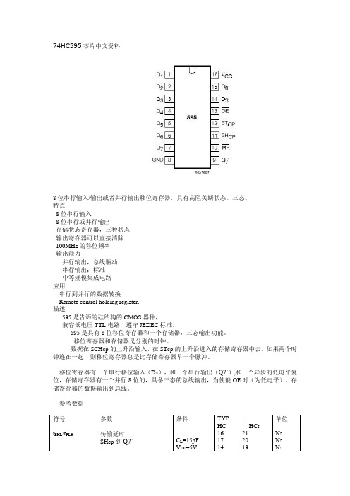
74HC595/74HCT595
它是带控制端的8位串行输入并行输入的移位寄存器,具有3态输出。
特点
➢8位串行输入
➢8位串行或并行输出
➢带有3态输出的存储寄存器
➢移位寄存器具有清零控制端
➢100MHz移位输出频率
➢输出能力:并行输出,总线驱动;串行输出,标准输出
应用
串行数据转并行
远程控制保持寄存器
相关描述
74HC/HCT595是高速硅栅CMOS元件与低功耗肖特基TTL引脚兼容。
它们符合JEDEC第7A号标准。
“595”是一个带存储器的8级串行移位寄存器,有3态输出。
移位寄存器以及存储寄存器有独立的时钟输入端。
当SH_CP端接收一个上跳沿时数据会发生移位。
当ST_CP端接收一个上跳沿时,移位寄存器中的数据将被送入存储寄存器。
当SH_CP端和ST_CP端短接时,移位寄存器当中所存储的数据将会永远比存储寄存器中的数据状态早一个时钟周期。
移位寄存器有一个串行输入(DS端)以及一个标准的串行级联输出端(Q7’)。
该芯片的8位移位寄存器有一个复位引脚(MR,低电平有效)。
存储寄存器有8条并行的3态总线连接至输出引脚。
只要芯片的输出使能引脚(OE)处于低电平,芯片就实时将存储寄存器中的数据输出至输出引脚。
74HC595完整中文资料之欧阳美创编
74HC595芯片是一种串入并出的芯片,在电子显示屏制作当中有广泛的应用。
74HC595是8位串行输入/输出或者并行输出移位寄存器,具有高阻、关、断状态。
三态。
特点 8位串行输入 8位串行或并行输出存储状态寄存器,三种状态输出寄存器可以直接清除 100MHz的移位频率输出能力并行输出,总线驱动串行输出;标准中等规模集成电路应用串行到并行的数据转换 Remote c ontrol holding register. 描述 595是告诉的硅结构的CMOS 器件,兼容低电压TTL电路,遵守JEDEC标准。
595是具有8位移位寄存器和一个存储器,三态输出功能。
移位寄存器和存储器是分别的时钟。
数据在SCHcp的上升沿输入,在STcp的上升沿进入的存储寄存器中去。
如果两个时钟连在一起,则移位寄存器总是比存储寄存器早一个脉冲。
移位寄存器有一个串行移位输入(Ds),和一个串行输出(Q7’),和一个异步的低电平复位,存储寄存器有一个并行8位的,具备三态的总线输出,当使能OE时(为低电平),存储寄存器的数据输出到总线。
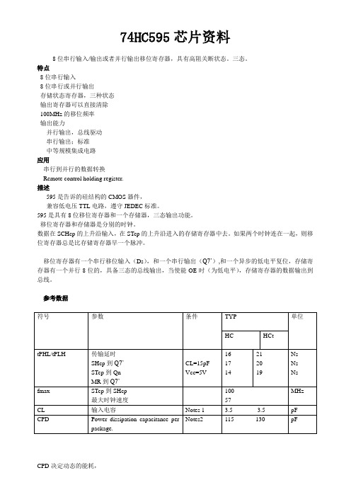
CPD决定动态的能耗, PD=CP D×VCC×f1+∑(CL×VCC2×f0) F1=输入频率,CL=输出电容 f0=输出频率(MHz) Vcc=电源电压引脚说明符号引脚描述内部结构结合引脚说明就能很快理解 595的工作情况引脚功能表:真值表:74595的数据端:QA--QH: 八位并行输出端,可以直接控制数码管的8个段。
QH': 级联输出端。
我将它接下一个595的SI端。
SI: 串行数据输入端。
74595的控制端说明:/SRCLR(10脚): 低点平时将移位寄存器的数据清零。
通常我将它接Vcc。
SRCK(11脚):上升沿时数据寄存器的数据移位。
QA-->QB-->QC-->...-->QH;下降沿移位寄存器数据不变。
(脉冲宽度:5V时,大于几十纳秒就行了。
74HC595芯片资料53971
74HC595芯片资料8位串行输入/输出或者并行输出移位寄存器,具有高阻关断状态。
三态。
特点8位串行输入8位串行或并行输出存储状态寄存器,三种状态输出寄存器可以直接清除100MHz的移位频率输出能力并行输出,总线驱动串行输出;标准中等规模集成电路应用串行到并行的数据转换Remote control holding register.描述595是告诉的硅结构的CMOS器件,兼容低电压TTL电路,遵守JEDEC标准。
595是具有8位移位寄存器和一个存储器,三态输出功能。
移位寄存器和存储器是分别的时钟。
数据在SCHcp的上升沿输入,在STcp的上升沿进入的存储寄存器中去。
如果两个时钟连在一起,则移位寄存器总是比存储寄存器早一个脉冲。
移位寄存器有一个串行移位输入(Ds),和一个串行输出(Q7’),和一个异步的低电平复位,存储寄存器有一个并行8位的,具备三态的总线输出,当使能OE时(为低电平),存储寄存器的数据输出到总线。
参考数据CPD决定动态的能耗,PD=CPD×VCC×f1+∑(CL×VCC2×f0)F1=输入频率,CL=输出电容f0=输出频率(MHz)Vcc=电源电压功能表H=高电平状态L=低电平状态↑=上升沿↓=下降沿Z=高阻NC=无变化×=无效当MR为高电平,OE为低电平时,数据在SHCP上升沿进入移位寄存器,在STCP上升沿输出到并行端口。
/***************************************************************************************/ 给个74HC595的"慢动作"void WriteSIOByte(unsigned char val){unsigned char i;ACC = val;for (i = 8; i > 0; i --) {SRCLK = 0;//拉低74HC595时钟_rrca_();//右移一位数据SER = CY;//发送74HC595一位串行数据SRCLK = 1;//拉高74HC595时钟_nop_();//延时}SER = 1;//释放数据总线//以下3条指令若在多字节时,应该移入多字节全发送完后在执行此3条指令RCLK = 0;_nop_();//延时RCLK = 1;//打入并行数据}74ls595"速射"hotpowerfor(i = 0; i < buffsize; i ++){SBUF = siobuff[i];while(TI == 0);TI = 0;}RCLK = 0;_nop_();//延时RCLK = 1;//打入并行数据/************************************************************************/摘要:本文介绍了应用移位寄存器芯片74HC595实现LED动、静态显示的基本原理。
74ls595芯片中文资料
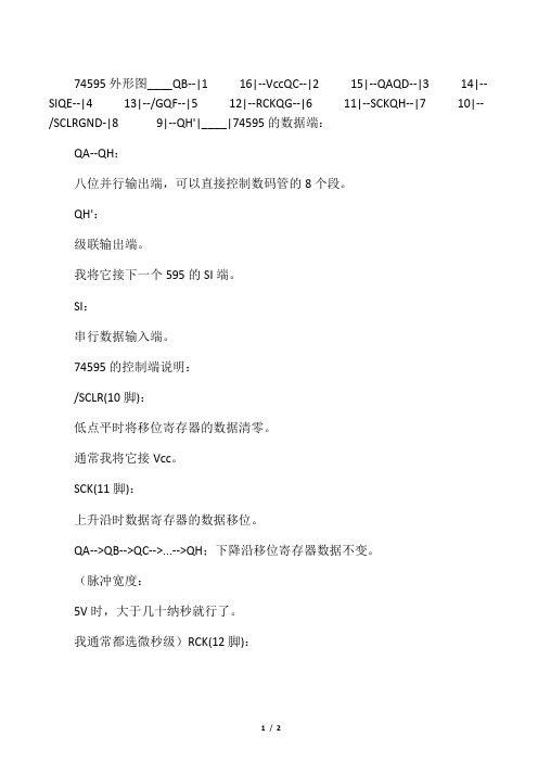
74595外形图____QB--|1 16|--VccQC--|2 15|--QAQD--|3 14|--SIQE--|4 13|--/GQF--|5 12|--RCKQG--|6 11|--SCKQH--|7 10|--/SCLRGND-|8 9|--QH'|____|74595的数据端:QA--QH:八位并行输出端,可以直接控制数码管的8个段。
QH':级联输出端。
我将它接下一个595的SI端。
SI:串行数据输入端。
74595的控制端说明:/SCLR(10脚):低点平时将移位寄存器的数据清零。
通常我将它接Vcc。
SCK(11脚):上升沿时数据寄存器的数据移位。
QA-->QB-->QC-->...-->QH;下降沿移位寄存器数据不变。
(脉冲宽度:5V时,大于几十纳秒就行了。
我通常都选微秒级)RCK(12脚):上升沿时移位寄存器的数据进入数据存储寄存器,下降沿时存储寄存器数据不变。
通常我将RCK置为低点平,当移位结束后,在RCK端产生一个正脉冲(5V 时,大于几十纳秒就行了。
我通常都选微秒级),更新显示数据。
/G(13脚):高电平时禁止输出(高阻态)。
如果单片机的引脚不紧张,用一个引脚控制它,可以方便地产生闪烁和熄灭效果。
比通过数据端移位控制要省时省力。
注:74164和74595功能相仿,都是8位串行输入转并行输出移位寄存器。
74164的驱动电流(25mA)比74595(35mA)的要小,14脚封装,体积也小一些。
74595的主要优点是具有数据存储寄存器,在移位的过程中,输出端的数据可以保持不变。
这在串行速度慢的场合很有用处,数码管没有闪烁感。
与164只有数据清零端相比,595还多有输出端时能/禁止控制端,可以使输出为高阻态。
另外,据网上报价,贴片164每只1元钱,贴片5950.8元/只。
74HC595史上最全的中文资料【中为电科】

X X 注:
X X
H L L L
L H H H
X H X X
L Q6S NC Q6S
Z NC QnS QnS
清空移位寄存器,并行输出高阻态 移位寄存器数据分别移动一位; 第 6 位数据 移入 Q7S 移位寄存器的内容传给存储寄存器并输出 移位寄存器的所有数据移动一位; 移位寄存 器中的所有数据转入存储寄存器并输出
7. 8. 9. 10. 11. 12. 13.
1 / 15
科技效法自然 中为电科
74HC595;74HCT595
8 位串行输入,串行或并行输出移位寄存器,输出具有锁存、三态功能
1. 简介
74HC595、 74HCT595 是一款高速硅栅 (Si‐gate) COMS 器件, 并且与低压肖特基 TTL (LSTTL) 兼容。它们符合 JEDEC 7A 号文件标准。 74HC595、74HCT595 是一个 8 位串行并且带有存储寄存器和三态输出的移位寄存器, 存储寄存器和移位寄存器同步于不同的时钟。 数据在移位寄存器时钟(SHCP)的正跳变下移动,在存储寄存器时钟(STCP)的正跳 变下数据由移位寄存器转存到存储寄存器。假如 SHCP 和 STCP 被连在一起,移位寄存器将 总是超前于存储寄存器一个时钟脉冲。 移位寄存器有一个串行输入端(DS) ,还有一个用于级联的串行输出端。8 位移位寄存 器可以异步复位 (低电平复位) 。 存储寄存器有一个 8 位三态并行输出端。 当输出使能端 (OE) 被使能(低有效)数据将从存储寄存器中输出至器件引脚。
4 / 15
科技效法自然 中为电科
6. 引脚定义
6.1 引脚图
图 4 引脚定义 6.2 引脚描述 符号 Q1 Q2 Q3 Q4 Q5 Q6 Q7 GND Q7S MR SHCP STCP OE DS Q0 Vcc 引脚号 1 2 3 4 5 6 7 8 9 10 11 12 13 14 15 16 地(0V) 数据串行输出 复位(低有效) 移位寄存器时钟(输入) 存储寄存器时钟(输入) 输出使能(低有效) 数据串行输入 数据并行输出 0 电源 数据并行输出 1 ~ 7 描述
74hc595资料
74HC595芯片中文资料8位串行输入/输出或者并行输出移位寄存器,具有高阻关断状态。
三态。
特点8位串行输入8位串行或并行输出存储状态寄存器,三种状态输出寄存器可以直接清除100MHz的移位频率输出能力并行输出,总线驱动串行输出;标准中等规模集成电路应用串行到并行的数据转换Remote control holding register.描述595是告诉的硅结构的CMOS器件,兼容低电压TTL电路,遵守JEDEC标准。
595是具有8位移位寄存器和一个存储器,三态输出功能。
移位寄存器和存储器是分别的时钟。
数据在SCHcp的上升沿输入,在STcp的上升沿进入的存储寄存器中去。
如果两个时钟连在一起,则移位寄存器总是比存储寄存器早一个脉冲。
移位寄存器有一个串行移位输入(Ds),和一个串行输出(Q7’),和一个异步的低电平复位,存储寄存器有一个并行8位的,具备三态的总线输出,当使能OE时(为低电平),存储寄存器的数据输出到总线。
参考数据符号参数条件TYP单位HC HCtt PHL/t PLH传输延时SHcp到Q7’C L=15pFVcc=5V 161714212019NsNsNsC PD 决定动态的能耗,P D =C PD ×V CC ×f 1+∑(C L ×V CC 2×f 0)F 1=输入频率,C L =输出电容 f 0=输出频率(MHz ) Vcc=电源电压 引脚说明 符号 引脚 描述 Q0…Q7 15, 1, 7 并行数据输出 GND 8 地 Q7’ 9 串行数据输出 MR 10 主复位(低电平) SH CP 11 移位寄存器时钟输入 ST CP 12 存储寄存器时钟输入 OE 13 输出有效(低电平) D S 14 串行数据输入 V CC 16 电源 功能表输入 输出功能SH CP ST CP OE MR D S Q7’ Q n× × L ↓ × L NC MR 为低电平时紧紧影响移位寄存器× ↑ L L × L L 空移位寄存器到输出寄存器 × × H L × L Z 清空移位寄存器,并行输出为高阻状态↑ × L H H Q 6’ NC 逻辑高电平移入移位寄存器状态0,包含所有的移位寄存器状态移入,例如,以前的状态6(内部Q6”)出现在串行输出位。
74HC595D中文资料_数据手册_参数
74HC595D中⽂资料_数据⼿册_参数74HC595; 74HCT5958-bit serial-in, serial or parallel-out shift register with outputlatches; 3-stateRev. 6 — 12 December 2011Product data sheet1. General descriptionThe 74HC595; 74HCT595 are high-speed Si-gate CMOS devices and are pin compatible with Low-power Schottky TTL (LSTTL). They are specified in compliance with JEDEC standard No.7A.The 74HC595; 74HCT595 are 8-stage serial shift registers with a storage register and3-state outputs. The registers have separate clocks.Data is shifted on the positive-going transitions of the shift register clock input (SHCP). The data in each register is transferred to the storage register on a positive-going transition of the storage register clock input (STCP). If both clocks are connected together, the shift register will always be one clock pulse ahead of the storage register.The shift register has a serial input (DS) and a serial standard output (Q7S) for cascading. It is also provided with asynchronous reset (active LOW) for all 8 shift register stages. The storage register has 8 parallel 3-state bus driver outputs. Data in the storage register appears at the output whenever the output enable input (OE) is LOW.2. Features and benefits8-bit serial input8-bit serial or parallel outputStorage register with 3-state outputsShift register with direct clear100MHz (typical) shift out frequencyESD protection:◆HBM JESD22-A114F exceeds2000V◆MM JESD22-A115-A exceeds200VMultiple package optionsSpecified from -40C to+85C and from -40C to+125C3. ApplicationsSerial-to-parallel data conversionRemote control holding register3-state4. Ordering information5. Functional diagramTable 1.Ordering informationType numberPackageTemperature rangeName DescriptionVersion 74HC595N -40?C to +125?CDIP16plastic dual in-line package; 16leads (300mil)SOT38-474HCT595N 74HC595D -40?C to +125?CSO16plastic small outline package; 16leads;body width 3.9mmSOT109-174HCT595D 74HC595DB -40?C to +125?CSSOP16plastic shrink small outline package; 16leads; body width 5.3mmSOT338-174HCT595DB 74HC595PW -40?C to +125?CTSSOP16plastic thin shrink small outline package; 16leads; body width 4.4mmSOT403-174HCT595PW 74HC595BQ -40?C to +125?CDHVQFN16plastic dual in-line compatible thermal enhanced very thin quad flat package; no leads; 16terminals; body 2.5 ? 3.5 ? 0.85 mmSOT763-174HCT595BQ3-state3-state 6. Pinning information3-state6.2Pin descriptionTable 2.Pin description Symbol Pin DescriptionQ11parallel data output 1Q22parallel data output 2Q33parallel data output 3Q44parallel data output 4Q55parallel data output 5Q66parallel data output 6Q77parallel data output 7 GND8ground (0 V)Q7S9serial data outputMR10master reset (active LOW)OE13output enable input (active LOW)DS14serial data inputQ015parallel data output 0V CC16supply voltage7. Functional descriptionTable 3.Function table[1]Control Input Output FunctionSHCP STCP OE MR DS Q7S QnX X L L X L NC a LOW-level on MR only affects the shift registersX↑L L X L L empty shift register loaded into storage registerX X H L X L Z shift register clear; parallel outputs in high-impedance OFF-state↑X L H H Q6S NC logic HIGH-level shifted into shift register stage 0. Contents of all shift register stages shifted through, e.g. previous state of stage 6(internal Q6S) appears on the serial output (Q7S).X↑L H X NC QnS contents of shift register stages (internal QnS) are transferred to the storage register and parallel output stages↑↑L H X Q6S QnS contents of shift register shifted through; previous contents of the shift register is transferred to the storage register and the paralleloutput stages[1]H=HIGH voltage state;L=LOW voltage state;↑=LOW-to-HIGH transition;X=don’t care;NC=no change;Z=high-impedance OFF-state.3-state8. Limiting valuesTable 4.Limiting valuesIn accordance with the Absolute Maximum Rating System (IEC 60134). Voltages are referenced to GND (ground = 0 V). Symbol Parameter Conditions Min Max UnitV CC supply voltage-0.5+7VI IK input clamping current V I < -0.5V or V I>V CC+0.5 V-±20mAI OK output clamping current V O<-0.5V or V O > V CC + 0.5 V-±20mAI O output current V O=-0.5V to (V CC+0.5V)pin Q7S-±25mApins Qn-±35mAI CC supply current-70mAI GND ground current-70-mAT stg storage temperature-65+150?CP tot total power dissipationDIP16 package[1]-750mWSO16 package[2]-500mWSSOP16 package[3]-500mWTSSOP16 package[3]-500mWDHVQFN16 package[4]-500mW[1]For DIP16 package: P tot derates linearly with 12mW/K above 70 ?C.[2]For SO16 package: P tot derates linearly with 8mW/K above 70 ?C.[3]For SSOP16 and TSSOP16 packages: P tot derates linearly with 5.5mW/K above 60 ?C.9. Recommended operating conditions10. Static characteristicsTable 5.Recommended operating conditionsSymbol ParameterConditions74HC59574HCT595UnitMinTyp Max Min Typ Max V CC supply voltage 2.0 5.0 6.0 4.5 5.0 5.5V V I input voltage 0-V CC 0-V CC V V O output voltage 0-V CC 0-V CC V ?t/?Vinput transition rise and fall rateV CC = 2.0 V --625---ns/V V CC = 4.5 V - 1.67139- 1.67139ns/V V CC = 6.0 V--83---ns/V T ambambient temperature-40+25+125-40+25+125C Table 6.Static characteristicsAt recommended operating conditions; voltages are referenced to GND (ground =0V).Symbol ParameterConditions-40?C to +85?C -40?C to +125?C UnitMinTypMaxMinMax74HC595V IHHIGH-level input voltageV CC =2.0V 1.5 1.2- 1.5-V V CC =4.5V 3.15 2.4- 3.15-V V CC =6.0VV CC =2.0V -0.80.5-0.5V V CC =4.5V - 2.1 1.35- 1.35V V CC =6.0V- 2.81.8- 1.8VV OHHIGH-level output voltageV I =V IH or V IL all outputsI O =-20µA; V CC =2.0V 1.9 2.0- 1.9-V I O =-20µA; V CC =4.5V 4.4 4.5- 4.4-V I O =-20µA; V CC =6.0V 5.96.0- 5.9-VQ7S outputI O =-4mA; V CC =4.5V 3.84 4.32- 3.7-V I O =-5.2mA; V CC =6.0V 5.345.81- 5.2-VQn bus driver outputs I O =-6mA; V CC =4.5V 3.84 4.32- 3.7-V I O =-7.8mA; V CC =6.0V5.345.81- 5.2-V3-stateV OL LOW-leveloutput voltage V I=V IH or V ILall outputsI O=20µA; V CC=2.0V-00.1-0.1V I O=20µA; V CC=4.5V-00.1-0.1V I O=20µA; V CC=6.0V-00.1-0.1V Q7S output I O=4mA;V CC=4.5V-0.150.33-0.4V I O=5.2mA;V CC=6.0V-0.160.33-0.4V Qn bus driver outputsI O=6mA;V CC=4.5V-0.150.33-0.4V I O=7.8mA;V CC=6.0V-0.160.33-0.4VI I input leakagecurrentV I=V CC or GND; V CC=6.0V--±1.0-±1.0µAI OZ OFF-state--80-160µAC I inputcapacitance- 3.5---pF 74HCT595V IH HIGH-levelinput voltageV CC=4.5V to 5.5V 2.0 1.6- 2.0-VV IL LOW-levelinput voltageV CC=4.5V to 5.5V- 1.20.8-0.8VV OH HIGH-leveloutput voltage V I=V IH or V IL; V CC=4.5Vall outputsI O=-20µA 4.4 4.5- 4.4-V Q7S outputI O=-4mA 3.84 4.32- 3.7-V Qn bus driver outputsI O=-6mA 3.7 4.32- 3.7-VV OL LOW-leveloutput voltage V I=V IH or V IL; V CC=4.5Vall outputsI O=20µA-00.1-0.1V Q7S outputI O=4.0mA-0.150.33-0.4V Qn bus driver outputsI O=6.0mA-0.160.33-0.4VI I input leakagecurrent V I=V CC or GND; V CC=5.5V--±1.0-±1.0µATable 6.Static characteristics …continuedAt recommended operating conditions; voltages are referenced to GND (ground=0V). Symbol Parameter Conditions-40?C to +85?C-40?C to +125?C UnitMin Typ Max Min Max3-stateI OZ OFF-state--80-160µAI CC additionalsupply current per input pin; I O=0A; V I=V CC-2.1V; other inputs at V CC or GND;V CC=4.5V to5.5Vpins MR, SHCP, STCP, OE-150675-735µA pin DS-25113-123µAC I inputcapacitance - 3.5---pFTable 6.Static characteristics …continuedAt recommended operating conditions; voltages are referenced to GND (ground=0V).Symbol Parameter Conditions-40?C to +85?C-40?C to +125?C UnitMin Typ Max Min Max3-state 11. Dynamic characteristicsTable 7.Dynamic characteristicsVoltages are referenced to GND (ground = 0 V); for test circuit see Figure14.Symbol Parameter Conditions25 ?C-40?C to+85 ?C-40?C to+125 ?C UnitMin Typ[1]Max Min Max Min Max74HC595t pd propagationdelay SHCP to Q7S; see Figure9[2]V CC = 2 V-52160-200-240ns V CC = 4.5 V-1932-40-48ns V CC = 6 V-1527-34-41ns STCP to Qn; see Figure10[2] V CC = 2 V-55175-220-265ns V CC = 4.5 V-2035-44-53ns V CC = 6 V-1630-37-45ns MR to Q7S; see Figure12[3] V CC = 2 V-47175-220-265ns V CC = 4.5 V-1735-44-53ns V CC = 6 V-1430-37-45nst en enable time OE to Qn; see Figure13[4]V CC = 2 V-47150-190-225nsV CC = 4.5 V-1730-38-45nsV CC = 6 V-1426-33-38ns t dis disable time OE to Qn; see Figure13[5]V CC = 2 V-41150-190-225nsV CC = 4.5 V-1530-38-45nsV CC = 6 V-1227-33-38ns t W pulse width SHCP HIGH or LOW;V CC = 4.5 V156-19-22-nsV CC = 6 V135-16-19-nsSTCP HIGH or LOW;see Figure10V CC = 2 V7511-95-110-nsV CC = 4.5 V154-19-22-nsV CC = 6 V133-16-19-nsMR LOW; see Figure12V CC = 2 V7517-95-110-nsV CC = 4.5 V156-19-22-nsV CC = 6 V135-16-19-ns3-statet suset-up timeDS to SHCP; see Figure 10V CC = 2 V 5011-65-75-ns V CC = 4.5 V 104-13-15-ns V CC = 6 V 9 3-11-13-nsSHCP to STCP; see Figure 11V CC = 2 V 7522-95-110-ns V CC = 4.5 V 158-19-22-ns V CC = 6 V 137-16-19-ns t hhold timeDS to SHCP; see Figure 11V CC = 2 V 3-6-3-3-ns V CC = 4.5 V 3-2-3-3-ns V CC = 6 V3-2-3-3-ns t recrecovery timeMR to SHCP; see Figure 12V CC = 2 V 50-19-65-75-ns V CC = 4.5 V 10-7-13-15-ns V CC = 6 V 9-6-11-13f maxmaximum frequencySHCP or STCP; see Figure 9 and 10V CC = 2 V 930- 4.8-4-MHz V CC = 4.5 V 3091-24-20-MHz V CC = 6 V35108-28-24-MHz C PDpower dissipation capacitancef i = 1 MHz; V I =GND to V CC [6][7]-115-----pF74HCT595; V CC = 4.5 V to 5.5 V t pdpropagation delay SHCP to Q7S; see Figure 9[2]-2542-53-63ns STCP to Qn; see Figure 10[2]-2440-50-60ns MR to Q7S; see Figure 12[3]-2340-50-60ns t en enable time OE to Qn; see Figure 13[4]-2135-44-53ns t dis disable time OE to Qn; see Figure 13[5] -1830-38-45ns t Wpulse widthSHCP HIGH or LOW;see Figure 9166-20-24-ns STCP HIGH or LOW; see Figure 10165-20-24-ns MR LOW; see Figure 12208-25-30-ns t suset-up timeDS to SHCP; see Figure 10165-20-24-ns SHCP to STCP; see Figure 11168-20-24-ns t hhold timeDS to SHCP; see Figure 113-2-3-nsTable 7.Dynamic characteristics …continuedVoltages are referenced to GND (ground = 0 V); for test circuit see Figure 14.Symbol Parameter Conditions25 ?C -40?C to +85 ?C -40?C to +125 ?C Unit Min Typ [1]Max Min Max Min Max3-state[1]Typical values are measured at nominal supply voltage.[2]t pd is the same as t PHL and t PLH .[3]t pd is the same as t PHL only.[4]t en is the same as t PZL and t PZH .[5]t dis is the same as t PLZ and t PHZ .[6]C PD is used to determine the dynamic power dissipation (P D in µW).P D =C PD ?V CC 2?f i +∑(C L ?V CC 2?f o )where:f i=input frequency in MHz;f o =output frequency in MHz;∑(C L ?V CC 2?f o )=sum of outputs;C L =output load capacitance in pF;V CC =supply voltage in V.[7]All 9outputs switching.12. Waveformst rec recovery time MR to SHCP; see Figure 1210-7-13-15-ns f max maximum frequencySHCP and STCP; see Figure 9 and 103052-24-20-MHz C PDpower dissipation capacitancef i = 1 MHz; V I =GND to V CC [6] [7]-130-----pFTable 7.Dynamic characteristics …continuedVoltages are referenced to GND (ground = 0 V); for test circuit see Figure 14.Symbol Parameter Conditions25 ?C -40?C to +85 ?C -40?C to +125 ?C Unit Min Typ [1]Max Min Max Min Max3-stateTable 8.Measurement points Type Input OutputV M V M74HC5950.5V CC0.5V CC 74HCT595 1.3V 1.3V3-stateTable 9.Test data74HC595V CC6ns50 pF1kΩopen GND V CC74HCT5953V6ns50 pF1kΩopen GND V CC3-state 13. Package outlineDIP16: plastic dual in-line package; 16 leads (300 mil)SOT38-4Fig 15.Package outline SOT38-4 (DIP16)3-state SO16: plastic small outline package; 16 leads; body width 3.9 mm SOT109-1Fig 16.Package outline SOT109-1 (SO16)3-state SSOP16: plastic shrink small outline package; 16 leads; body width 5.3 mm SOT338-1Fig 17.Package outline SOT338-1 (SSOP16)3-state TSSOP16: plastic thin shrink small outline package; 16 leads; body width 4.4 mm SOT403-1Fig 18.Package outline SOT403-1 (TSSOP16)。
74HC595D中文资料_数据手册_参数

NXP Semiconductors
74HC595; 74HCT595
8-bit serial-in, serial or parallel-out shift register with output latches; 3-state
11 12
SHCP STCP
14 DS
Q7S 9 15
All information provided in this document is subject to legal disclaimers.
Rev. 6 — 12 December 2011
© NXP B.V. 2011. All rights reserved.
3 of 24
NXP Semiconductors
Fig 7. Pin configuration for DHVQFN16
74HC_HCT595
Product data sheet
All information provided in this document is subject to legal disclaimers.
Rev. 6 — 12 December 2011
16 VCC 15 Q0 14 DS 13 OE 12 STCP 11 SHCP 10 MR 9 Q7S
001aao241
Fig 5. Pin configuration DIP16, SO16
74HC595 74HCT595
Q1 1 Q2 2 Q3 3 Q4 4 Q5 5 Q6 6 Q7 7 GND 8
5. Functional diagram
14 DS 11 SHCP 10 MR
8-STAGE SHIFT REGISTER
- 1、下载文档前请自行甄别文档内容的完整性,平台不提供额外的编辑、内容补充、找答案等附加服务。
- 2、"仅部分预览"的文档,不可在线预览部分如存在完整性等问题,可反馈申请退款(可完整预览的文档不适用该条件!)。
- 3、如文档侵犯您的权益,请联系客服反馈,我们会尽快为您处理(人工客服工作时间:9:00-18:30)。
PACKAGING INFORMATIONOrderable Device Status(1)PackageType PackageDrawingPins PackageQtyEco Plan(2)Lead/Ball Finish MSL Peak Temp(3)SN74AHCT595D ACTIVE SOIC D1640Green(RoHS&no Sb/Br)CU NIPDAU Level-1-260C-UNLIMSN74AHCT595DBR ACTIVE SSOP DB162000Green(RoHS&no Sb/Br)CU NIPDAU Level-1-260C-UNLIMSN74AHCT595DBRE4ACTIVE SSOP DB162000Green(RoHS&no Sb/Br)CU NIPDAU Level-1-260C-UNLIMSN74AHCT595DE4ACTIVE SOIC D1640Green(RoHS&no Sb/Br)CU NIPDAU Level-1-260C-UNLIMSN74AHCT595DR ACTIVE SOIC D162500Green(RoHS&no Sb/Br)CU NIPDAU Level-1-260C-UNLIMSN74AHCT595DRE4ACTIVE SOIC D162500Green(RoHS&no Sb/Br)CU NIPDAU Level-1-260C-UNLIMSN74AHCT595N ACTIVE PDIP N1625Pb-Free(RoHS)CU NIPDAU N/A for Pkg TypeSN74AHCT595NE4ACTIVE PDIP N1625Pb-Free(RoHS)CU NIPDAU N/A for Pkg TypeSN74AHCT595NSR ACTIVE SO NS162000Green(RoHS&no Sb/Br)CU NIPDAU Level-1-260C-UNLIMSN74AHCT595NSRE4ACTIVE SO NS162000Green(RoHS&no Sb/Br)CU NIPDAU Level-1-260C-UNLIMSN74AHCT595PW ACTIVE TSSOP PW1690Green(RoHS&no Sb/Br)CU NIPDAU Level-1-260C-UNLIMSN74AHCT595PWE4ACTIVE TSSOP PW1690Green(RoHS&no Sb/Br)CUNIPDAU Level-1-260C-UNLIMSN74AHCT595PWR ACTIVE TSSOP PW162000Green(RoHS&no Sb/Br)CU NIPDAU Level-1-260C-UNLIMSN74AHCT595PWRE4ACTIVE TSSOP PW162000Green(RoHS&no Sb/Br)CU NIPDAU Level-1-260C-UNLIM(1)The marketing status values are defined as follows:ACTIVE:Product device recommended for new designs.LIFEBUY:TI has announced that the device will be discontinued,and a lifetime-buy period is in effect.NRND:Not recommended for new designs.Device is in production to support existing customers,but TI does not recommend using this part in a new design.PREVIEW:Device has been announced but is not in production.Samples may or may not be available.OBSOLETE:TI has discontinued the production of the device.(2)Eco Plan-The planned eco-friendly classification:Pb-Free(RoHS),Pb-Free(RoHS Exempt),or Green(RoHS&no Sb/Br)-please check /productcontent for the latest availability information and additional product content details.TBD:The Pb-Free/Green conversion plan has not been defined.Pb-Free(RoHS):TI's terms"Lead-Free"or"Pb-Free"mean semiconductor products that are compatible with the current RoHS requirements for all6substances,including the requirement that lead not exceed0.1%by weight in homogeneous materials.Where designed to be soldered at high temperatures,TI Pb-Free products are suitable for use in specified lead-free processes.Pb-Free(RoHS Exempt):This component has a RoHS exemption for either1)lead-based flip-chip solder bumps used between the die and package,or2)lead-based die adhesive used between the die and leadframe.The component is otherwise considered Pb-Free(RoHS compatible)as defined above.Green(RoHS&no Sb/Br):TI defines"Green"to mean Pb-Free(RoHS compatible),and free of Bromine(Br)and Antimony(Sb)based flame retardants(Br or Sb do not exceed0.1%by weight in homogeneous material)(3)MSL,Peak Temp.--The Moisture Sensitivity Level rating according to the JEDEC industry standard classifications,and peak solder temperature.Important Information and Disclaimer:The information provided on this page represents TI's knowledge and belief as of the date that it is 18-Jul-2006provided.TI bases its knowledge and belief on information provided by third parties,and makes no representation or warranty as to the accuracy of such information.Efforts are underway to better integrate information from third parties.TI has taken and continues to take reasonable steps to provide representative and accurate information but may not have conducted destructive testing or chemical analysis on incoming materials and chemicals.TI and TI suppliers consider certain information to be proprietary,and thus CAS numbers and other limited information may not be available for release.In no event shall TI's liability arising out of such information exceed the total purchase price of the TI part(s)at issue in this document sold by TI to Customer on an annualbasis.18-Jul-2006IMPORTANT NOTICETexas Instruments Incorporated and its subsidiaries (TI) reserve the right to make corrections, modifications, enhancements, improvements, and other changes to its products and services at any time and to discontinue any product or service without notice. Customers should obtain the latest relevant information before placing orders and should verify that such information is current and complete. All products are sold subject to TI’s terms and conditions of sale supplied at the time of order acknowledgment.TI warrants performance of its hardware products to the specifications applicable at the time of sale in accordance with TI’s standard warranty. T esting and other quality control techniques are used to the extent TI deems necessary to support this warranty. Except where mandated by government requirements, testing of all parameters of each product is not necessarily performed.TI assumes no liability for applications assistance or customer product design. Customers are responsible for their products and applications using TI components. T o minimize the risks associated with customer products and applications, customers should provide adequate design and operating safeguards.TI does not warrant or represent that any license, either express or implied, is granted under any TI patent right, copyright, mask work right, or other TI intellectual property right relating to any combination, machine, or process in which TI products or services are used. Information published by TI regarding third-party products or services does not constitute a license from TI to use such products or services or a warranty or endorsement thereof. Use of such information may require a license from a third party under the patents or other intellectual property of the third party, or a license from TI under the patents or other intellectual property of TI.Reproduction of information in TI data books or data sheets is permissible only if reproduction is without alteration and is accompanied by all associated warranties, conditions, limitations, and notices. Reproduction of this information with alteration is an unfair and deceptive business practice. TI is not responsible or liable for such altered documentation.Resale of TI products or services with statements different from or beyond the parameters stated by TI for that product or service voids all express and any implied warranties for the associated TI product or service and is an unfair and deceptive business practice. TI is not responsible or liable for any such statements. Following are URLs where you can obtain information on other Texas Instruments products and application solutions:Products ApplicationsAmplifiers Audio /audioData Converters Automotive /automotiveDSP Broadband /broadbandInterface Digital Control /digitalcontrolLogic Military /militaryPower Mgmt Optical Networking /opticalnetwork Microcontrollers Security /securityLow Power Wireless /lpw Telephony /telephonyVideo & Imaging /videoWireless /wirelessMailing Address:Texas InstrumentsPost Office Box 655303 Dallas, Texas 75265Copyright 2006, Texas Instruments Incorporated。