H5N2306PF中文资料
上海钽电容规格

上海钽电容规格一、产品概述钽电容是一种高性能的电子元器件,具有高频响应、低失真、低温漂、长寿命等优点。
上海钽电容是一款高品质的钽电容产品,广泛应用于通信、计算机、航空航天等领域。
二、产品特点1. 高频响应:上海钽电容具有快速的响应速度,适用于高频率的信号传输。
2. 低失真:上海钽电容具有良好的线性特性,能够减少信号失真。
3. 低温漂:上海钽电容在不同温度下保持稳定的性能,能够适应各种环境要求。
4. 长寿命:上海钽电容采用优质材料和先进工艺制造,具有长期稳定的使用寿命。
三、产品参数1. 容量范围:0.1μF-1000μF2. 工作电压范围:4V-50V3. 容差范围:±10%、±20%4. 工作温度范围:-55℃~+125℃5. 封装形式:SMD、插件式四、产品应用1. 通信设备:上海钽电容广泛应用于手机、平板电脑、路由器等通信设备中,能够提高信号传输质量。
2. 计算机设备:上海钽电容在计算机主板、显卡等设备中应用广泛,能够提高系统性能和稳定性。
3. 航空航天:上海钽电容具有良好的耐高温性能和抗辐射性能,适用于航空航天领域的各种应用。
五、产品认证上海钽电容通过了ISO9001质量管理体系认证和ISO14001环境管理体系认证,产品符合RoHS环保要求。
六、质量保证1. 上海钽电容采用优质材料和先进工艺制造,确保产品的品质稳定可靠。
2. 上海钽电容实行严格的质量控制标准,每一批产品都经过严格测试和检验。
3. 上海钽电容提供完善的售后服务,对产品出现的任何问题都进行及时处理。
七、包装与交付1. 包装方式:上海钽电容采用防静电包装,在运输过程中能够有效避免静电干扰对产品造成的影响。
2. 交付时间:上海钽电容能够按照客户要求提供定制化服务,交付时间根据订单量和生产进度而定。
八、售后服务1. 上海钽电容提供全面的售后服务,对因产品质量问题造成的损失进行赔偿。
2. 上海钽电容提供技术支持和咨询服务,为客户解决使用过程中遇到的问题。
焊机常用电源芯片
焊机常用电源芯片(中英文实用版)英文文档:Title: Common Power Supply Chips for Welding MachinesWelding machines are essential tools in various industries, and their performance is highly dependent on the quality and type of power supply chips used.Power supply chips play a crucial role in regulating and stabilizing the power output of welding machines, ensuring consistent and reliable welding operations.One commonly used power supply chip in welding machines is the integrated circuit (IC) controller.This chip is responsible for managing the flow of electricity and maintaining the desired output voltage and current levels.It protects the machine from overcurrent, overvoltage, and short-circuit conditions, ensuring safe and reliable operation.Another essential type of power supply chip used in welding machines is the voltage regulator.This chip ensures that the voltage supplied to the welding torch and other components remains stable, regardless of fluctuations in the input voltage.Voltage regulators are available in different types, such as linear regulators and switching regulators, each offering specific advantages in terms of efficiency and size.Furthermore, power supply chips for welding machines often includeprotection features, such as overtemperature protection and undervoltage lockout.These features help prevent damage to the welding machine due to excessive heat or low voltage conditions, extending the lifespan of the equipment.In conclusion, the choice of power supply chips for welding machines is crucial for achieving optimal performance, reliability, and safety.By selecting the appropriate power supply chips, welders can ensure efficient and consistent welding operations, even in challenging environments.中文文档:标题:焊接机常用电源芯片焊接机是各种行业中不可或缺的工具,其性能在很大程度上取决于所使用电源芯片的质量和类型。
SGM2306中文资料

Fig 12. Gate Charge Waveform
/
Any changing of specification will not be informed individual
01-Jun-2002 Rev. A
Page 4 of 4
SOT-89
Features
* Capable Of 2.5V Gate Drive * Lower On-Resistance
Millimeter Min. Max. 4.4 4.6 4.05 4.25 1.50 1.70 1.30 1.50 2.40 2.60 0.89 1.20 Millimeter Min. Max. 3.00 REF. 1.50 REF. 0.40 0.52 1.40 1.60 0.35 0.41 5° TYP. 0.70 REF.
Description
The SGM2306 utilized advanced processing techniques to achieve the lowest possible on-resistance, extremely efficient and cost-effectiveness device.The SGM2306 is universally used for all commercial-industrial applications.
REF. A B C D E F
REF. G H I J K L M
D
G
S
Absolute Maximum Ratings
Parameter
Drain-Source Voltage Gate-Source Voltage Continuous Drain Current, VGS@4.5V Continuous Drain Current, VGS@4.5V Pulsed Drain Current
AM2306N规格书

PRODUCT SUMMARY
VDS (V)
rDS(on) m(Ω)
30
58 @ VGS = 10V
82 @ VGS = 4.5V
SOT-23 Top View
ID (A) 3.5 3.0
D
•
Low rDS(on) Provides Higher Efficiency and
Extends Battery Life
C A P A C IT A N C E (p F
ID, DRAIN CURRENT (A)
30 VDS = 5V
25
20
TA = -55oC
25oC 125oC
15
10
5
0
0.5
1.5
2.5
3.5
4.5
VGS, GATE TO SOURCE VOLTAGE (V)
Figure 2. Body Diode Forward Voltage Variation with Source Current and Temperature
朱小姐 Q Q :23 55 60 80 68 T el :13510 6668 20 w w w .cx tk e.c om
深圳市信德意电子有限公司
Analog Power
AM2306NE
ID , D R A IN C U R R E N T (A
Analog Power
AM2306NE
N-Channel 30-V (D-S) MOSFET
These miniature surface mount MOSFETs utilize High Cell Density process. Low rDS(on) assures minimal power loss and conserves energy, making this device ideal for use in power management circuitry. Typical applications are PWMDC-DC converters, power management in portable and battery-powered products such as computers, printers, battery charger, telecommunication power system, and telephones power system.
高频小功率电源技术参数及应用领域

高频小功率电源型号简介
输出电流:0~50000A 输出电压:0~1000V 输入电压:三相AC380V±10%, 50~60HZ等 稳压精度:≤1% 稳流精度:≤1% 额定效率:≥85% 操作环境:-10~40℃ 存放温度: -20~50℃ 冷却系统: 全水冷或风水冷 运行状况: 满负荷24小时运行 IP等级:全水冷IP54
全水冷ip54高频小功率电源高频小功率电源高频小功率电源高频小功率电源特点特点点采用五柱芯变压器六相半波整流器取代了平衡电抗器从而主配线相对简洁损耗减少电磁噪音较低比一般三柱变压器节能10以采用水冷结构功率部件通水冷却冷却效果好能够延迟功率元件的使用寿命
高频小功率电源
指示灯不亮原因
台兴智能电源
护等级可达IP54。
高频小功率电源特点特点
À
· 产品外形美观,结构合理,有多种外形选择。
À
· 稳压、稳流控制模式。
À
· 可提供RS485接口或者标准的4~20MA、0~10V、0~5V控制信号。
À
· 采用普通自来水冷却即可,推荐采用去离子水。
高频小功率电源特点说明
À À
À
À
故障原因有以下几点: a、电源线没有插好,有可能是电源插座不牢固,或者是电源线,插座等 的损坏。这时应该插牢插座,接好电源,可用电笔检测是哪一个出现了问题。 b、整流器总开关未闭合,这个可能是因为工作人员一时忘记造成的,所 以请闭合开关闸就可以了。 c、还有就是三相电源中缺相时也会造成电镀整流器的无法正常供电,应及 时检查维修。
高频小功率电源
高频小功率电源特点点
· 采用五柱芯变压器 ,六相半波整流器取代了平衡电抗器,从而主配 线相对简洁,损耗减少,电磁噪音较低,比一般三柱变压器节能10%以 上。 · 采用水冷结构,功率部件通水冷却,冷却效果好,能够延迟功 率元件的使用寿命。
AP2306N中文资料

N-CHANNEL ENHANCEMENT MODE POWER MOSFET▼ Capable of 2.5V gate drive BV DSS20V ▼ Lower on-resistance R DS(ON)32m Ω▼ Surface mount packageI D5.3ADescriptionAbsolute Maximum RatingsSymbol Units V DS V V GSV I D @T A =25℃A I D @T A =70℃A I DMA P D @T A =25℃W W/℃T STG ℃T J℃Symbol Value Unit Rthj-aThermal Resistance Junction-ambient 3Max.90℃/WData and specifications subject to change without notice200509032AP2306NParameterRating Drain-Source Voltage 20Gate-Source VoltageContinuous Drain Current 3, V GS @ 4.5V 5.3Continuous Drain Current 3, V GS @ 4.5V 4.3Pulsed Drain Current 1,210Total Power Dissipation 1.38-55 to 150Operating Junction Temperature Range-55 to 150Linear Derating Factor 0.01Thermal DataParameterStorage Temperature Range± 12DGSSOT-23Advanced Power MOSFETs utilized advanced processing techniques to achieve the lowest possible on-resistance, extremely efficient and cost-effectiveness device.The SOT-23 package is universally used for all commercial-industrial applications.Electrical Characteristics@T j =25o C(unless otherwise specified)Symbol ParameterTest ConditionsMin.Typ.Max.Units BV DSSDrain-Source Breakdown VoltageV GS =0V, I D =250uA 20--V ΔB V DSS /ΔT jBreakdown Voltage Temperature Coefficient Reference to 25℃, I D =1mA-0.1-V/℃R DS(ON)Static Drain-Source On-ResistanceV GS =10V, I D =5.5A --27m ΩV GS =4.5V, I D =5.3A --32m ΩV GS =2.5V, I D =2.6A --50m ΩV GS =1.8V, I D =1.0A--90m ΩV GS(th)Gate Threshold Voltage V DS =V GS , I D =250uA 0.5--V g fs Forward TransconductanceV DS =5V, I D =5.3A -13-S I DSS Drain-Source Leakage Current (T j =25o C)V DS =20V, V GS =0V --1uA Drain-Source Leakage Current (T j =55o C)V DS =16V ,V GS =0V --10uA I GSS Gate-Source Leakage V GS =--nA Q g Total Gate Charge 2I D =5.3A -8.7-nC Q gs Gate-Source Charge V DS =10V - 1.5-nC Q gd Gate-Drain ("Miller") Charge V GS =4.5V - 3.6-nC t d(on)Turn-on Delay Time 2V DS =15V -6-ns t r Rise TimeI D =1A-14-ns t d(off)Turn-off Delay Time R G =2Ω,V GS =10V -18.4-ns t f Fall Time R D =15Ω- 2.8-ns C iss Input Capacitance V GS =0V -603-pF C oss Output CapacitanceV DS =15V -144-pF C rssReverse Transfer Capacitancef=1.0MHz-111-pFSource-Drain DiodeSymbol ParameterTest ConditionsMin.Typ.Max.Units V SD Forward On Voltage 2I S =1.2A, V GS =0V -- 1.2V trr Reverse Recovery TimeI S =5A, V GS =0V,-16.8-ns QrrReverse Recovery ChargedI/dt=100A/µs-11-nCNotes:1.Pulse width limited by Max. junction temperature.2.Pulse width <300us , duty cycle <2%.3.Surface mounted on 1 in 2 copper pad of FR4 board ; 270℃/W when mounted on min. copper pad.± 12V ±100AP2306NFig 1. Typical Output CharacteristicsFig 4. Normalized On-Resistancev.s. Junction TemperatureFig 5. Forward Characteristic ofFig 6. Gate Threshold Voltage v.s.Reverse DiodeJunction TemperatureFig 7. Gate Charge Characteristics Fig 8. Typical Capacitance CharacteristicsFig 9. Maximum Safe Operating Area Fig 10. Effective Transient Thermal ImpedanceFig 11. Switching Time Circuit Fig 12. Gate Charge CircuitAP2306N。
矽钢H50与H23有什么区别
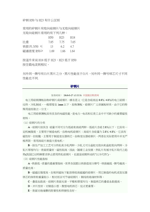
矽钢H50与H23有什么区别常用的矽钢片有取向硅钢片与无取向硅钢片无取向硅钢片常用的有下列几种:H50 H23 H18比重7.85 7.75 7.65铁损P1.5/50 ≤13 6.2 4.7磁通密度B50≥ 1.69 1.66 1.64按温升来说H18低于H23,H23低于H50按空载电流则相反。
另外同一牌号有白片黑片之分,黑片性能优于白片。
另外同一牌号铁芯尺寸不同性能也不同.矽钢片发布时间:2010-3-27 15:55:31 中国废旧物资网电工用硅钢薄板俗称矽钢片或硅钢片。
顾名思义,它是含硅高达0.8%-4.8%的电工硅钢,经热、冷轧制成。
一般厚度在1mm以下,故称薄板。
硅钢片广义讲属板材类,由于它的特殊用途而独立一分支。
电工用硅钢薄板具有优良的电磁性能,是电力、电讯和仪表工业中不可缺少的重要磁性材料。
(1)硅钢片的分类A、硅钢片按其含硅量不同可分为低硅和高硅两种。
低硅片含硅2.8%以下,它具有一定机械强度,主要用于制造电机,俗称电机硅钢片;高硅片含硅量为2.8%-4.8%,它具有磁性好,但较脆,主要用于制造变压器铁芯,俗称变压器硅钢片。
两者在实际使用中并无严格界限,常用高硅片制造大型电机。
B、按生产加工工艺可分热轧和冷轧两种,冷轧又可分晶粒无取向和晶粒取向两种。
冷轧片厚度均匀、表面质量好、磁性较高,因此,随着工业发展,热轧片有被冷轧片取代之趋势(我国已经明确要求停止使用热轧硅钢片,也就是前期所说的"以冷代热")。
(2)硅钢片性能指标A、铁损低。
质量的最重要指标,世界各国都以铁损值划分牌号,铁损越低,牌号越高,质量也高。
B、磁感应强度高。
在相同磁场下能获得较高磁感的硅钢片,用它制造的电机或变压器铁芯的体积和重量较小,相对而言可节省硅钢片、铜线和绝缘材料等。
C、叠装系数高。
硅钢片表面光滑,平整和厚度均匀,制造铁芯的叠装系数提高。
D、冲片性好。
对制造小型、微型电机铁芯,这点更重要。
RF2306中文资料

Operating Voltage Operating Current
Operating Current Range
DC to 2000
18
19.5
22
19.5
21
23.5
3.5 < 2:1
< 2:1 +20
+10
+12
+15
> 20
3.7
28
35
42
20 to 65
MHz dB dB dB
Ordering Information
RF2306
General Purpose Amplifier
RF2306 PCBA Fully Assembled Evaluation Board
Functional Block Diagram
RF Micro Devices, Inc. 7625 Thorndike Road Greensboro, NC 27409, USA
Tel (336) 664 1233 Fax (336) 664 0454
Rev B2 000228
4-63
元器件交易网
RF2306
Absolute Maximum Ratings
Parameter
Rating
Unit
Supply Current Input RF Power Operating Ambient Temperature Storage Temperature
RF OUT
Application Schematic
22 pF
RF IN
1
2
3
4
- 1、下载文档前请自行甄别文档内容的完整性,平台不提供额外的编辑、内容补充、找答案等附加服务。
- 2、"仅部分预览"的文档,不可在线预览部分如存在完整性等问题,可反馈申请退款(可完整预览的文档不适用该条件!)。
- 3、如文档侵犯您的权益,请联系客服反馈,我们会尽快为您处理(人工客服工作时间:9:00-18:30)。
H5N2306PF
Silicon N Channel MOS FET
High Speed Power Switching
REJ03G0031-0200Z
Rev.2.00
Jun.25.2004 Features
•Low on-resistance
•Low leakage current
•High speed switching
Outline
Absolute Maximum Rating
(Ta = 25°C) Item Symbol Rating Unit
Drain to source voltage V DSS230V
Gate to source voltage V GSS±30V
Drain current I D30A
Drain peak current I D (pulse)Note1160A
Body-drain diode reverse drain
I DR30A
current
I DR (pulse)Note1160A
Body-drain diode reverse drain
peak current
Avalanche current I AP Note315A
Channel dissipation Pch Note260W
Channel to case thermal impedanceθch-c 2.08°C/W
Channel temperature Tch150°C
Storage temperature Tstg–55 to +150°C
Notes: 1.PW ≤ 10 µs, duty cycle ≤ 1%
2.Value at Tc = 25°C
3. STch = 25°C, Tch ≤ 150°C
Electrical Characteristics
(Ta = 25°C) Item Symbol Min Typ Max Unit Test condition
Drain to Source breakdown
voltage
V(BR)DSS230——V I D = 10 mA, V GS = 0
Zero gate voltage drain current I DSS——1µA V DS = 230 V, V GS = 0
Gate to source leak current I GSS——±0.1µA V GS = ±30 V, V DS = 0
Gate to source cutoff voltage V GS(off) 2.5— 4.0V V DS = 10 V, I D = 1 mA Forward transfer admittance|yfs|1932—S I D = 15 A, V DS = 10 V Note4 Static drain to source on state
resistance
R DS(on)—0.0410.052ΩI D = 15 A, V GS = 10 V Note4
Input capacitance Ciss—3500—pF Output capacitance Coss—480—pF Reverse transfer capacitance Crss—40—pF V DS = 25 V V GS = 0
f = 1 MHz
Turn-on deray time td(on)—45—ns Rise time tr—110—ns Turn-off delay time td(off)—125—ns Fall time tf—80—ns I D = 15 A V GS = 10 V R L = 6.7 ΩRg = 10 Ω
Total gate charge Qg—70—nC Gate to source charge Qgs—17—nC Gate to drain charge Qgd—24—nC V DD = 160 V V GS = 10 V I D = 30 A
Body-drain diode forward
voltage
V DF—0.9 1.4V I F = 30 A, V GS = 0 Note4
Body-drain diode reverse
recovery time
trr—170—ns
Body-drain diode reverse recovery charge Qrr— 1.0—µC
I F = 30 A, V GS = 0
diF/dt = 100 A/µs
Notes: 4.Pulse test
Main Characteristics
Package Dimensions
Ordering Information
Part Name Quantity Shipping Container
H5N2306PF-E30 pcs Plastic magazine
Note:For some grades, production may be terminated. Please contact the Renesas sales office to check the state of production before ordering the product.
RENESAS SALES OFFICES
Renesas Technology America, Inc.
450 Holger Way, San Jose, CA 95134-1368, U.S.A
Tel: <1> (408) 382-7500 Fax: <1> (408) 382-7501
Renesas Technology Europe Limited.
Dukes Meadow, Millboard Road, Bourne End, Buckinghamshire, SL8 5FH, United Kingdom
Tel: <44> (1628) 585 100, Fax: <44> (1628) 585 900
Renesas Technology Europe GmbH
Dornacher Str. 3, D-85622 Feldkirchen, Germany
Tel: <49> (89) 380 70 0, Fax: <49> (89) 929 30 11
Renesas Technology Hong Kong Ltd.
7/F., North Tower, World Finance Centre, Harbour City, Canton Road, Hong Kong
Tel: <852> 2265-6688, Fax: <852> 2375-6836
Renesas Technology Taiwan Co., Ltd.
FL 10, #99, Fu-Hsing N. Rd., Taipei, Taiwan
Tel: <886> (2) 2715-2888, Fax: <886> (2) 2713-2999
Renesas Technology (Shanghai) Co., Ltd.
26/F., Ruijin Building, No.205 Maoming Road (S), Shanghai 200020, China
Tel: <86> (21) 6472-1001, Fax: <86> (21) 6415-2952
Renesas Technology Singapore Pte. Ltd.
1, Harbour Front Avenue, #06-10, Keppel Bay Tower, Singapore 098632
Tel: <65> 6213-0200, Fax: <65> 6278-8001
Colophon .1.0。