ATF2500C_08中文资料
AT24C08

1Features•Low-voltage and Standard-voltage Operation –2.7 (V CC = 2.7V to 5.5V)–1.8 (V CC = 1.8V to 5.5V)•Internally Organized 128 x 8 (1K), 256 x 8 (2K), 512 x 8 (4K),1024 x 8 (8K) or 2048 x 8 (16K)•Two-wire Serial Interface•Schmitt Trigger, Filtered Inputs for Noise Suppression •Bidirectional Data Transfer Protocol•100 kHz (1.8V) and 400 kHz (2.7V , 5V) Compatibility •Write Protect Pin for Hardware Data Protection•8-byte Page (1K, 2K), 16-byte Page (4K, 8K, 16K) Write Modes •Partial Page Writes Allowed•Self-timed Write Cycle (5 ms max)•High-reliability–Endurance: 1 Million Write Cycles –Data Retention: 100 Years•Automotive Grade and Lead-free/Halogen-free Devices Available •8-lead PDIP , 8-lead JEDEC SOIC, 8-lead MAP , 5-lead SOT23,8-lead TSSOP and 8-ball dBGA2 Packages•Die Sales: Wafer Form, Waffle Pack and Bumped WafersDescriptionThe AT24C01A/02/04/08A/16A provides 1024/2048/4096/8192/16384 bits of serial electrically erasable and programmable read-only memory (EEPROM) organized as 128/256/512/1024/2048 words of 8 bits each. The device is optimized for use in many industrial and commercial applications where low-power and low-voltage operation are essential. The AT24C01A/02/04/08A/16A is available in space-saving 8-lead PDIP , 8-lead JEDEC SOIC, 8-lead MAP , 5-lead SOT23 (AT24C01A/AT24C02/AT24C04), 8-lead TSSOP , and 8-ball dBGA2 packages and is accessed via a Two-wire serial inter-face. In addition, the entire family is available in 2.7V (2.7V to 5.5V) and 1.8V (1.8V to 5.5V) versions.Table 1. Pin ConfigurationPin Name Function A0 - A2Address Inputs SDA Serial Data SCL Serial Clock Input WP Write Protect NC No Connect GND Ground VCCPower Supply8-lead SOIC8-lead PDIP8-lead MAPBottom View 5-lead SOT238-ball dBGA2Bottom View 8-lead TSSOP2AT24C01A/02/04/08A/16A0180V–SEEPR–8/05Figure 1. Block DiagramAbsolute Maximum RatingsOperating T emperature..................................–55°C to +125°C *NOTICE:Stresses beyond those listed under “Absolute Maximum Ratings” may cause permanent dam-age to the device. This is a stress rating only and functional operation of the device at these or any other conditions beyond those indicated in the operational sections of this specification is not implied. Exposure to absolute maximum rating conditions for extended periods may affect device reliability.Storage T emperature.....................................–65°C to +150°C Voltage on Any Pinwith Respect to Ground....................................–1.0V to +7.0V Maximum Operating Voltage ..........................................6.25V DC Output Current........................................................5.0 mA元器件配套服务中心丗3AT24C01A/02/04/08A/16A0180V–SEEPR–8/05Pin DescriptionSERIAL CLOCK (SCL): The SCL input is used to positive edge clock data into each EEPROM device and negative edge clock data out of each device.SERIAL DATA (SDA): The SDA pin is bidirectional for serial data transfer. This pin is open-drain driven and may be wire-ORed with any number of other open-drain or open-collector devices.DEVICE/PAGE ADDRESSES (A2, A1, A0): The A2, A1 and A0 pins are device address inputs that are hard wired for the AT24C01A and the AT24C02. As many as eight 1K/2K devices may be addressed on a single bus system (device addressing is discussed in detail under the Device Addressing section).The AT24C04 uses the A2 and A1 inputs for hard wire addressing and a total of four 4K devices may be addressed on a single bus system. The A0 pin is a no connect.The AT24C08A only uses the A2 input for hardwire addressing and a total of two 8K devices may be addressed on a single bus system. The A0 and A1 pins are no connects.The AT24C16A does not use the device address pins, which limits the number of devices on a single bus to one. The A0, A1 and A2 pins are no connects.WRITE PROTECT (WP): The AT24C01A/02/04/08A/16A has a Write Protect pin that provides hardware data protection. The Write Protect pin allows normal Read/Write operations when connected to ground (GND). When the Write Protect pin is connected to V CC , the write protection feature is enabled and operates as shown in Table 2.Table 2. Write ProtectMemory OrganizationAT24C01A, 1K SERIAL EEPROM: Internally organized with 16 pages of 8 bytes each,the 1K requires a 7-bit data word address for random word addressing.AT24C02, 2K SERIAL EEPROM: Internally organized with 32 pages of 8 bytes each,the 2K requires an 8-bit data word address for random word addressing.AT24C04, 4K SERIAL EEPROM: Internally organized with 32 pages of 16 bytes each,the 4K requires a 9-bit data word address for random word addressing.AT24C08A, 8K SERIAL EEPROM: Internally organized with 64 pages of 16 bytes each,the 8K requires a 10-bit data word address for random word addressing.AT24C16A, 16K SERIAL EEPROM: Internally organized with 128 pages of 16 bytes each, the 16K requires an 11-bit data word address for random word addressing.WP Pin Status Part of the Array Protected24C01A 24C0224C0424C08A 24C16A At V CC Full (1K) ArrayFull (2K) ArrayFull (4K) ArrayFull (8K) ArrayFull (16K) ArrayAt GNDNormal Read/Write Operations4AT24C01A/02/04/08A/16A0180V–SEEPR–8/05Note:1.This parameter is characterized and is not 100% tested.Note:1.V IL min and V IH max are reference only and are not tested.Table 3. Pin Capacitance (1)Applicable over recommended operating range from T A = 25°C, f = 1.0 MHz, V CC = +1.8VSymbol Test ConditionMax Units Conditions C I/O Input/Output Capacitance (SDA)8pF V I/O = 0V C IN Input Capacitance (A 0, A 1, A 2, SCL)6pFV IN = 0VTable 4. DC CharacteristicsApplicable over recommended operating range from: T AI = –40°C to +85°C, V CC = +1.8V to +5.5V, V CC =+1.8V to +5.5V (unless otherwise noted)Symbol Parameter Test ConditionMin TypMax Units V CC1Supply Voltage 1.8 5.5V V CC2Supply Voltage 2.7 5.5V V CC3Supply Voltage4.55.5V I CC Supply Current V CC = 5.0V READ at 100 kHz 0.4 1.0mA I CC Supply Current V CC = 5.0V WRITE at 100 kHz 2.0 3.0mA I SB1Standby Current V CC = 1.8V V IN = V CC or V SS 0.6 3.0µA I SB2Standby Current V CC = 2.5V V IN = V CC or V SS 1.4 4.0µA I SB3Standby Current V CC = 2.7V V IN = V CC or V SS 1.6 4.0µA I SB4Standby Current V CC = 5.0V V IN = V CC or V SS 8.018.0µA I LI Input Leakage Current V IN = V CC or V SS 0.10 3.0µA I LO Output Leakage Current V OUT = V CC or V SS0.05 3.0µA V IL Input Low Level (1)–0.6V CC x 0.3V V IH Input High Level (1)V CC x 0.7V CC + 0.5V V OL2Output Low Level V CC = 3.0V I OL = 2.1 mA 0.4V V OL1Output Low Level V CC = 1.8VI OL = 0.15 mA 0.2V5AT24C01A/02/04/08A/16A0180V–SEEPR–8/05Note:1.This parameter is characterized.Table 5. AC CharacteristicsApplicable over recommended operating range from T AI = –40°C to +85°C, V CC = +1.8V to +5.5V, V CC = +2.7V to +5.5V,CL = 1 TTL Gate and 100pF (unless otherwise noted)Symbol Parameter1.8-volt2.7, 5.0-volt Units MinMax MinMax f SCL Clock Frequency, SCL 100400kHz t LOW Clock Pulse Width Low 4.7 1.2µs t HIGH Clock Pulse Width High 4.00.6µs t I Noise Suppression Time (1)10050ns t AA Clock Low to Data Out Valid 0.1 4.50.10.9µs t BUF Time the bus must be free before a new transmission can start (1) 4.7 1.2µs t HD.ST A Start Hold Time 4.00.6µs t SU.ST A Start Setup Time 4.70.6µs t HD.DA T Data In Hold Time 00µs t SU.DAT Data In Setup Time 200100ns t R Inputs Rise Time (1) 1.00.3µs t F Inputs Fall Time (1)300300ns t SU.STO Stop Setup Time 4.70.6µs t DH Data Out Hold Time 10050ns t WRWrite Cycle Time 55ms Endurance (1) 5.0V , 25°C, Byte Mode1M 1MWrite Cycles6AT24C01A/02/04/08A/16A0180V–SEEPR–8/05Device OperationCLOCK and DATA TRANSITIONS: The SDA pin is normally pulled high with an exter-nal device. Data on the SDA pin may change only during SCL low time periods (see Figure 4 on page 7). Data changes during SCL high periods will indicate a start or stop condition as defined below.START CONDITION: A high-to-low transition of SDA with SCL high is a start condition which must precede any other command (see Figure 5 on page 8).STOP CONDITION: A low-to-high transition of SDA with SCL high is a stop condition.After a read sequence, the stop command will place the EEPROM in a standby power mode (see Figure 5 on page 8).ACKNOWLEDGE: All addresses and data words are serially transmitted to and from the EEPROM in 8-bit words. The EEPROM sends a zero to acknowledge that it has received each word. This happens during the ninth clock cycle.STANDBY MODE: The AT24C01A/02/04/08A/16A features a low-power standby mode which is enabled: (a) upon power-up and (b) after the receipt of the STOP bit and the completion of any internal operations.MEMORY RESET: After an interruption in protocol, power loss or system reset, any 2-wire part can be reset by following these steps:1.Clock up to 9 cycles.2.Look for SDA high in each cycle while SCL is high.3.Create a start condition.7AT24C01A/02/04/08A/16A0180V–SEEPR–8/05Bus TimingFigure 2. SCL: Serial Clock, SDA: Serial Data I/OWrite Cycle TimingFigure 3. SCL: Serial Clock, SDA: Serial Data I/ONote:1.The write cycle time t WR is the time from a valid stop condition of a write sequence to the end of the internal clear/write cycle.Figure 4.Data Validity8AT24C01A/02/04/08A/16A0180V–SEEPR–8/05Figure 5. Start and Stop DefinitionFigure 6.Output Acknowledge9AT24C01A/02/04/08A/16A0180V–SEEPR–8/05Device AddressingThe 1K, 2K, 4K, 8K and 16K EEPROM devices all require an 8-bit device address word following a start condition to enable the chip for a read or write operation (refer to Figure 7).The device address word consists of a mandatory one, zero sequence for the first four most significant bits as shown. This is common to all the EEPROM devices.The next 3 bits are the A2, A1 and A0 device address bits for the 1K/2K EEPROM.These 3 bits must compare to their corresponding hard-wired input pins.The 4K EEPROM only uses the A2 and A1 device address bits with the third bit being a memory page address bit. The two device address bits must compare to their corre-sponding hard-wired input pins. The A0 pin is no connect.The 8K EEPROM only uses the A2 device address bit with the next 2 bits being for memory page addressing. The A2 bit must compare to its corresponding hard-wired input pin. The A1 and A0 pins are no connect.The 16K does not use any device address bits but instead the 3 bits are used for mem-ory page addressing. These page addressing bits on the 4K, 8K and 16K devices should be considered the most significant bits of the data word address which follows.The A0, A1 and A2 pins are no connect.The eighth bit of the device address is the read/write operation select bit. A read opera-tion is initiated if this bit is high and a write operation is initiated if this bit is low.Upon a compare of the device address, the EEPROM will output a zero. If a compare is not made, the chip will return to a standby state.Write OperationsBYTE WRITE: A write operation requires an 8-bit data word address following the device address word and acknowledgment. Upon receipt of this address, the EEPROM will again respond with a zero and then clock in the first 8-bit data word. Following receipt of the 8-bit data word, the EEPROM will output a zero and the addressing device, such as a microcontroller, must terminate the write sequence with a stop condi-tion. At this time the EEPROM enters an internally timed write cycle, t WR , to the nonvolatile memory. All inputs are disabled during this write cycle and the EEPROM will not respond until the write is complete (see Figure 8 on page 11).PAGE WRITE: The 1K/2K EEPROM is capable of an 8-byte page write, and the 4K, 8K and 16K devices are capable of 16-byte page writes.A page write is initiated the same as a byte write, but the microcontroller does not send a stop condition after the first data word is clocked in. Instead, after the EEPROM acknowledges receipt of the first data word, the microcontroller can transmit up to seven (1K/2K) or fifteen (4K, 8K, 16K) more data words. The EEPROM will respond with a zero after each data word received. The microcontroller must terminate the page write sequence with a stop condition (see Figure 9 on page 11).The data word address lower three (1K/2K) or four (4K, 8K, 16K) bits are internally incremented following the receipt of each data word. The higher data word address bits are not incremented, retaining the memory page row location. When the word address,internally generated, reaches the page boundary, the following byte is placed at the beginning of the same page. If more than eight (1K/2K) or sixteen (4K, 8K, 16K) data words are transmitted to the EEPROM, the data word address will “roll over” and previ-ous data will be overwritten.10AT24C01A/02/04/08A/16A0180V–SEEPR–8/05ACKNOWLEDGE POLLING: Once the internally timed write cycle has started and the EEPROM inputs are disabled, acknowledge polling can be initiated. This involves sending a start condition followed by the device address word. The read/write bit is representative of the operation desired. Only if the internal write cycle has completed will the EEPROM respond with a zero allowing the read or write sequence to continue.ReadOperationsRead operations are initiated the same way as write operations with the exception that the read/write select bit in the device address word is set to one. There are three read operations:current address read, random address read and sequential read.CURRENT ADDRESS READ: The internal data word address counter maintains the last address accessed during the last read or write operation, incremented by one. This address stays valid between operations as long as the chip power is maintained. The address “roll over” during read is from the last byte of the last memory page to the first byte of the first page.The address “roll over” during write is from the last byte of the current page to the first byte of the same page.Once the device address with the read/write select bit set to one is clocked in and acknowl-edged by the EEPROM, the current address data word is serially clocked out. The microcontroller does not respond with an input zero but does generate a following stop condi-tion (see Figure 10 on page 12).RANDOM READ: A random read requires a “dummy” byte write sequence to load in the data word address. Once the device address word and data word address are clocked in and acknowledged by the EEPROM, the microcontroller must generate another start condition.The microcontroller now initiates a current address read by sending a device address with the read/write select bit high. The EEPROM acknowledges the device address and serially clocks out the data word. The microcontroller does not respond with a zero but does generate a fol-lowing stop condition (see Figure 11 on page 12).SEQUENTIAL READ: Sequential reads are initiated by either a current address read or a ran-dom address read. After the microcontroller receives a data word, it responds with an acknowledge. As long as the EEPROM receives an acknowledge, it will continue to increment the data word address and serially clock out sequential data words. When the memory address limit is reached, the data word address will “roll over” and the sequential read will con-tinue. The sequential read operation is terminated when the microcontroller does not respond with a zero but does generate a following stop condition (see Figure 12 on page 12).11AT24C01A/02/04/08A/16A0180V–SEEPR–8/05Figure 7. Device AddressFigure 8. Byte WriteFigure 9. Page Write(* = DON’T CARE bit for 1K)12AT24C01A/02/04/08A/16A0180V–SEEPR–8/05Figure 10. Current Address ReadFigure 11. Random Read(* = DON’T CARE bit for 1K)Figure 12.Sequential Read13AT24C01A/02/04/08A/16A0180V–SEEPR–8/05Notes:1.For2.7V devices used in the 4.5V to 5.5V range, please refer to performance values in the AC and DC characteristics table.2.“U” designates Green Package + RoHS compliant.3.Available in waffle pack and wafer form; order as SL719 for wafer form. Bumped die available upon request. Please contactSerial EEPROM Marketing.AT24C01A Ordering Information (1)Ordering Code Package Operation Range A T24C01A-10PI-2.7A T24C01A-10SI-2.7A T24C01A-10TI-2.78P38S18A2Industrial T emperature (–40°C to 85°C)A T24C01A-10PI-1.8A T24C01A-10SI-1.8A T24C01A-10TI-1.88P38S18A2Industrial T emperature (–40°C to 85°C)A T24C01A-10PU-2.7(2)A T24C01A-10PU-1.8(2)A T24C01A-10SU-2.7(2)A T24C01A-10SU-1.8(2)A T24C01A-10TU-2.7(2)A T24C01A-10TU-1.8(2)A T24C01A-10TSU-1.8(2)A T24C01AU3-10UU-1.8(2)A T24C01AY1-10YU-1.8(2)8P38P38S18S18A28A25TS18U318Y1Lead-free/Halogen-free/Industrial T emperature (–40°C to 85°C)A T24C01A-W2.7-11(3)A T24C01A-W1.8-11(3)Die Sale Die SaleIndustrial T emperature (–40°C to 85°C)Package Type8P38-lead, 0.300" Wide, Plastic Dual Inline Package (PDIP)8S18-lead, 0.150" Wide, Plastic Gull Wing Small Outline (JEDEC SOIC)8A28-lead, 4.4 mm Body, Plastic Thin Shrink Small Outline Package (TSSOP)8Y18-lead, 4.90 mm x 3.00 mm Body, Dual Footprint, Non-leaded, Miniature Array Package (MAP)5TS15-lead, 2.90 mm x 1.60 mm Body, Plastic Thin Shrink Small Outline Package (SOT23)8U3-18-ball, die Ball Grid Away Package (dBGA2)Options–2.7Low-voltage (2.7V to 5.5V)–1.8Low-voltage (1.8V to 5.5V)14AT24C01A/02/04/08A/16A0180V–SEEPR–8/05Notes:1.For2.7V devices used in the 4.5V to 5.5V range, please refer to performance values in the AC and DC characteristics table.2.“U” designates Green Package + RoHS compliant.3.Available in waffle pack and wafer form; order as SL719 for wafer form. Bumped die available upon request. Please contactSerial EEPROM Marketing.AT24C02 Ordering Information (1)Ordering Code Package Operation Range A T24C02-10PI-2.7A T24C02N-10SI-2.7A T24C02-10TI-2.78P38S18A2Industrial Temperature (–40°C to 85°C)A T24C02-10PI-1.8A T24C02N-10SI-1.8A T24C02-10TI-1.88P38S18A2Industrial Temperature (–40°C to 85°C)A T24C02-10PU-2.7(2)A T24C02-10PU-1.8(2)A T24C02N-10SU-2.7(2)A T24C02N-10SU-1.8(2)A T24C02-10TU-2.7(2)A T24C02-10TU-1.8(2)A T24C02Y1-10YU-1.8(2)A T24C02-10TSU-1.8(2)A T24C02U3-10UU-1.8(2)8P38P38S18S18A28A28Y15TS18U3-1Lead-free/Halogen-free/Industrial Temperature (–40°C to 85°C)A T24C02-W2.7-11(3)A T24C02-W1.8-11(3)Die Sale Die SaleIndustrial Temperature (–40°C to 85°C)Package Type8P38-lead, 0.300" Wide, Plastic Dual Inline Package (PDIP)8S18-lead, 0.150" Wide, Plastic Gull Wing Small Outline (JEDEC SOIC)8A28-lead, 4.4 mm Body, Plastic Thin Shrink Small Outline Package (TSSOP)8Y18-lead, 4.90 mm x 3.00 mm Body, Dual Footprint, Non-leaded, Miniature Array Package (MAP)5TS15-lead, 2.90 mm x 1.60 mm Body, Plastic Thin Shrink Small Outline Package (SOT23)8U3-18-ball, die Ball Grid Away Package (dBGA2)Options–2.7Low-voltage (2.7V to 5.5V)–1.8Low-voltage (1.8V to 5.5V)15AT24C01A/02/04/08A/16A0180V–SEEPR–8/05Notes:1.For2.7V devices used in the 4.5V to 5.5V range, please refer to performance values in the AC and DC characteristics table.2.“U” designates Green Package + RoHS compliant.3.Available in waffle pack and wafer form; order as SL719 for wafer form. Bumped die available upon request. Please contactSerial EEPROM Marketing.AT24C04 Ordering Information (1)Ordering Code Package Operation Range A T24C04-10PI-2.7A T24C04N-10SI-2.7A T24C04-10TI-2.78P38S18A2Industrial T emperature (–40°C to 85°C)A T24C04-10PI-1.8A T24C04N-10SI-1.8A T24C04-10TI-1.88P38S18A2Industrial T emperature (–40°C to 85°C)A T24C04-10PU-2.7(2)A T24C04-10PU-1.8(2)A T24C04N-10SU-2.7(2)A T24C04N-10SU-1.8(2)A T24C04-10TU-2.7(2)A T24C04-10TU-1.8(2)A T24C04Y1-10YU-1.8(2)A T24C04-10TSU-1.8(2)A T24C04U3-10UU-1.8(2)8P38P38S18S18A28A28Y15TS18U3-1Lead-free/Halogen-free/Industrial T emperature (–40°C to 85°C)A T24C04-W2.7-11(3)A T24C04-W1.8-11(3)Die Sale Die SaleIndustrial T emperature (–40°C to 85°C)Package Type8P38-lead, 0.300" Wide, Plastic Dual Inline Package (PDIP)8S18-lead, 0.150" Wide, Plastic Gull Wing Small Outline (JEDEC SOIC)8A28-lead, 4.4 mm Body, Plastic Thin Shrink Small Outline Package (TSSOP)8Y18-lead, 4.90 mm x 3.00 mm Body, Dual Footprint, Non-leaded, Miniature Array Package (MAP)5TS15-lead, 2.90 mm x 1.60 mm Body, Plastic Thin Shrink Small Outline Package (SOT23)8U3-18-ball, die Ball Grid Away Package (dBGA2)Options–2.7Low-voltage (2.7V to 5.5V)–1.8Low-voltage (1.8V to 5.5V)16AT24C01A/02/04/08A/16A0180V–SEEPR–8/05Notes:1.For2.7V devices used in the 4.5V to 5.5V range, please refer to performance values in the AC and DC characteristics table.2.“U” designates Green Package + RoHS compliant.3.Available in waffle pack and wafer form; order as SL719 for wafer form. Bumped die available upon request. Please contactSerial EEPROM Marketing.AT24C08A Ordering Information (1)Ordering Code PackageOperation Range A T24C08A-10PI-2.7A T24C08AN-10SI-2.7A T24C08A-10TI-2.78P38S18A2Industrial T emperature (–40°C to 85°C)A T24C08A-10PI-1.8A T24C08AN-10SI-1.8A T24C08A-10TI-1.88P38S18A2Industrial T emperature (–40°C to 85°C)A T24C08A-10PU-2.7(2)A T24C08A-10PU-1.8(2)A T24C08AN-10SU-2.7(2)A T24C08AN-10SU-1.8(2)A T24C08A-10TU-2.7(2)A T24C08A-10TU-1.8(2)A T24C08AY1-10YU-1.8(2)A T24C08AY5-10YU-1.8(2)A T24C08AU2-10UU-1.8(28P38P38S18S18A28A28Y18Y58U2-1Lead-free/Halogen-free/Industrial T emperature (−40°C to 85°C)A T24C08A-W2.7-11(3)A T24C08A-W1.8-11(3)Die Sale Die SaleIndustrial T emperature (−40°C to 85°C)Package Type8P38-pin, 0.300" Wide, Plastic Dual Inline Package (PDIP)8S18-lead, 0.150" Wide, Plastic Gull Wing Small Outline (JEDEC SOIC)8A28-lead, 4.4 mm Body, Plastic Thin Shrink Small Outline Package (TSSOP)8Y18-lead, 4.90 mm x 3.00 mm Body, Dual Footprint, Non-leaded, Miniature Array Package (MAP)8Y58-lead, 2.00 mm x 3.00 mm Body, Dual Footprint, Non-Leaded, Miniature Array Package (MAP)8U2-18-ball, die Ball Grid Array Package (dBGA2)Options−2.7Low Voltage (2.7V to 5.5V)−1.8Low Voltage (1.8V to 5.5V)17AT24C01A/02/04/08A/16A0180V–SEEPR–8/05Notes:1.For2.7V devices used in the 4.5V to 5.5V range, please refer to performance values in the AC and DC characteristics table.2.“U” designates Green Package + RoHS compliant.3.Available in waffle pack and wafer form; order as SL719 for wafer form. Bumped die available upon request. Please contactSerial EEPROM Marketing.AT24C16A Ordering Information (1)Ordering Code PackageOperation Range A T24C16A-10PI-2.7A T24C16AN-10SI-2.7A T24C16A-10TI-2.78P38S18A2Industrial T emperature (–40°C to 85°C)A T24C16A-10PI-1.8A T24C16AN-10SI-1.8A T24C16A-10TI-1.88P38S18A2Industrial T emperature (–40°C to 85°C)A T24C16A-10PU-2.7(2)A T24C16A-10PU-1.8(2)A T24C16AN-10SU-2.7(2)A T24C16AN-10SU-1.8(2)A T24C16A-10TU-2.7(2)A T24C16A-10TU-1.8(2)A T24C16AY1-10YU-1.8(2)A T24C16AY5-10YU-1.8(2)A T24C16AU2-10UU-1.8(2)8P38P38S18S18A28A28Y18Y58U2-1Lead-free/Halogen-free/Industrial T emperature (−40°C to 85°C)A T24C16A-W2.7-11(3)A T24C16A-W1.8-11(3)Die Sale Die SaleIndustrial T emperature (−40°C to 85°C)Package Type8P38-pin, 0.300" Wide, Plastic Dual Inline Package (PDIP)8S18-lead, 0.150" Wide, Plastic Gull Wing Small Outline (JEDEC SOIC)8A28-lead, 0.170" Wide, Thin Shrink Small Outline Package (TSSOP)8Y18-lead, 4.90 mm x 3.00 mm Body, Dual Footprint, Non-leaded, Miniature Array Package (MAP)8Y58-lead, 2.00 mm x 3.00 mm Body, Dual Footprint, Non-leaded, Miniature Array Package (MAP)8U2-18-ball, die Ball Grid Array Package (dBGA2)Options−2.7Low Voltage (2.7V to 5.5V)−1.8Low Voltage (1.8V to 5.5V)18AT24C01A/02/04/08A/16A0180V–SEEPR–8/05Packaging Information8P3 – PDIP19AT24C01A/02/04/08A/16A0180V–SEEPR–8/058S1 – JEDEC SOIC20AT24C01A/02/04/08A/16A0180V–SEEPR–8/058A2 – TSSOP21AT24C01A/02/04/08A/16A0180V–SEEPR–8/058Y1 – MAP22AT24C01A/02/04/08A/16A0180V–SEEPR–8/055TS1 – SOT2323AT24C01A/02/04/08A/16A0180V–SEEPR–8/058U3-1 – dBGA20180V–SEEPR–8/05Disclaimer: The information in this document is provided in connection with Atmel products. No license, express or implied, by estoppel or otherwise,to any intellectual property right is granted by this document or in connection with the sale of Atmel products. EXCEPT AS SET FORTH IN ATMEL ’S TERMS AND CONDI-TIONS OF SALE LOCATED ON ATMEL ’S WEB SITE, ATMEL ASSUMES NO LIABILITY WHATSOEVER AND DISCLAIMS ANY EXPRESS, IMPLIED OR STATUTORY WARRANTY RELATING TO ITS PRODUCTS INCLUDING, BUT NOT LIMITED TO, THE IMPLIED WARRANTY OF MERCHANTABILITY, FITNESS FOR A PARTICULAR PURPOSE, OR NON-INFRINGEMENT. IN NO EVENT SHALL ATMEL BE LIABLE FOR ANY DIRECT, INDIRECT, CONSEQUENTIAL, PUNITIVE, SPECIAL OR INCIDEN-TAL DAMAGES (INCLUDING, WITHOUT LIMITATION, DAMAGES FOR LOSS OF PROFITS, BUSINESS INTERRUPTION, OR LOSS OF INFORMATION) ARISING OUT OF THE USE OR INABILITY TO USE THIS DOCUMENT, EVEN IF ATMEL HAS BEEN ADVISED OF THE POSSIBILITY OF SUCH DAMAGES. Atmel makes no representations or warranties with respect to the accuracy or completeness of the contents of this document and reserves the right to make changes to specifications and product descriptions at any time without notice. Atmel does not make any commitment to update the information contained herein. Unless specifically provided otherwise, Atmel products are not suitable for, and shall not be used in, automotive applications. Atmel’s products are not intended, authorized, or warranted for use as components in applications intended to support or sustain life.Atmel CorporationAtmel Operations2325 Orchard Parkway San Jose, CA 95131, USA Tel: 1(408) 441-0311Fax: 1(408) 487-2600Regional HeadquartersEuropeAtmel SarlRoute des Arsenaux 41Case Postale 80CH-1705 Fribourg SwitzerlandTel: (41) 26-426-5555Fax: (41) 26-426-5500AsiaRoom 1219Chinachem Golden Plaza 77 Mody Road Tsimshatsui East Kowloon Hong KongTel: (852) 2721-9778Fax: (852) 2722-1369Japan9F, Tonetsu Shinkawa Bldg.1-24-8 ShinkawaChuo-ku, Tokyo 104-0033JapanTel: (81) 3-3523-3551Fax: (81) 3-3523-7581Memory2325 Orchard Parkway San Jose, CA 95131, USA Tel: 1(408) 441-0311Fax: 1(408) 436-4314Microcontrollers2325 Orchard Parkway San Jose, CA 95131, USA Tel: 1(408) 441-0311Fax: 1(408) 436-4314La Chantrerie BP 7060244306 Nantes Cedex 3, France Tel: (33) 2-40-18-18-18Fax: (33) 2-40-18-19-60ASIC/ASSP/Smart CardsZone Industrielle13106 Rousset Cedex, France Tel: (33) 4-42-53-60-00Fax: (33) 4-42-53-60-011150 East Cheyenne Mtn. Blvd.Colorado Springs, CO 80906, USA Tel: 1(719) 576-3300Fax: 1(719) 540-1759Scottish Enterprise Technology Park Maxwell BuildingEast Kilbride G75 0QR, Scotland Tel: (44) 1355-803-000Fax: (44) 1355-242-743RF/AutomotiveTheresienstrasse 2Postfach 353574025 Heilbronn, Germany Tel: (49) 71-31-67-0Fax: (49) 71-31-67-23401150 East Cheyenne Mtn. Blvd.Colorado Springs, CO 80906, USA Tel: 1(719) 576-3300Fax: 1(719) 540-1759Biometrics/Imaging/Hi-Rel MPU/High Speed Converters/RF DatacomAvenue de Rochepleine BP 12338521 Saint-Egreve Cedex, France Tel: (33) 4-76-58-30-00Fax: (33) 4-76-58-34-80Literature Requests/literature© Atmel Corporation 2005. All rights reserved. Atmel ®, logo and combinations thereof, Everywhere You Are ® and others, are registered trade-marks or trademarks of Atmel Corporation or its subsidiaries. Other terms and product names may be trademarks of others.。
cc2500中文
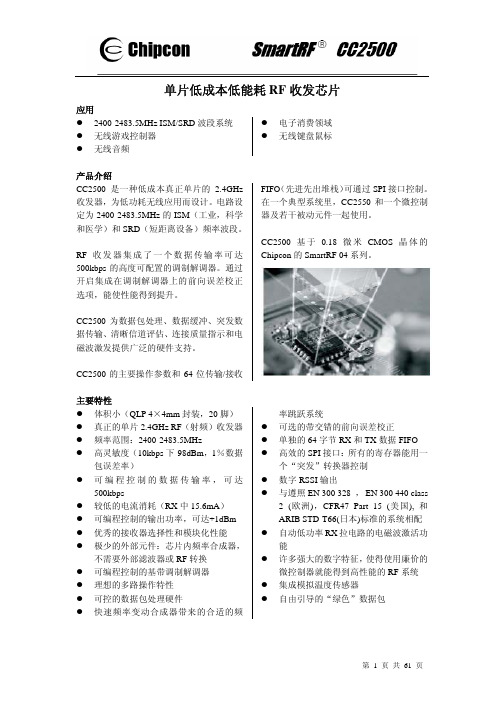
第 1 页 共 61 页
z 对数据包导向系统的灵活支持:对同步 词汇插入的芯片侦测,地址检查,灵活 的数据包长度及自动 CRC 处理
z 可编程信道滤波带宽 z OOK 和灵活的 ASK 整型支持 z 2-FSK 和 MSK 支持 z 自动频率补偿可用来调整频率合成器
到接收中间频率 z 对数据的可选自动白化处理 z 对现存通信协议的向后兼容的异步透
第 2 页 共 61 页
目录 1 缩写词 ....................................................................................................................... 2 2 绝对最大等级 ........................................................................................................... 5 3 工作条件 ................................................................................................................... 5 4 电气规范 ................................................................................................................... 6 5 常规特性 .............................................................................................
AT88SC0808C Atmel 密码型存储器数据手册说明书
AT88SC0808CAtmel CryptoMemory, 8-KbitSUMMARY DATASHEETFeatures • One of a family of nine devices with user memories from 1-Kbit to 256-Kbit •8-Kbit (1-Kbyte) EEPROM user memory• Eight 128-byte (1-Kbit) zones • Self-timed write cycle• Single byte or 16-byte page write mode • Programmable access rights for each zone• 2-Kbit configuration zone• 37-byte OTP area for user-defined codes• 160-byte area for user-defined keys and passwords •High security features• 64-bit mutual authentication protocol (under license of ELVA) • Encrypted checksum • Stream encryption• Four key sets for authentication and encryption • Eight sets of two 24-bit passwords • Anti-tearing function• Voltage and frequency monitor•Smart card features• ISO 7816 Class A (5V) or Class B (3V) operation• ISO 7816-3 asynchronous T = 0 protocol (Gemplus ®patent) * • Multiple zones, key sets and passwords for multi-application use • Synchronous 2-wire serial interface for faster device initialization * • Programmable 8-byte answer-to-reset register •ISO 7816-2 compliant modules•Embedded application features• Low voltage operation: 2.7V to 5.5V• Secure nonvolatile storage for sensitive system or user information • 2-wire serial interface• 1.0MHz compatibility for fast operation• Standard 8-lead plastic packages, green compliant (exceeds RoHS) •Same pinout as 2-wire Serial EEPROMs•High reliability• Endurance: 100,000 cycles • Data retention: 10 years • ESD protection: 4,000V min* Note: Modules available with either T=0 / 2-wire modes or 2-wire mode onlyThis is a summary document. The complete document is available on the Atmel website at .AT88SC0808C [SUMMARY DATASHEET]Atmel-2024MS-CryptoMem-AT88SC0808C-Datasheet-Summary_1220132Table 1. Pin AssignmentFigure 1.Pin Configuration1. DescriptionThe Atmel ®AT88SC0808C member of the Atmel CryptoMemory ®family is a high-performance secure memory providing 8-Kbits of user memory with advanced security and cryptographic features built in. The user memory is divided into eight 128-byte zones, each of which may be individually set with different security access rights or effectively combined together to provide space for one to eight data files.1.1 Smart Card ApplicationsThe AT88SC0808C provides high security, low cost, and ease of implementation without the need for a microprocessor operating system. The embedded cryptographic engine provides for dynamic and symmetric mutual authentication between the device and host, as well as performing stream encryption for all data and passwords exchanged between the device and host. Up to four unique key sets may be used for these operations. The AT88SC0808C offers the ability to communicate with virtually any smart card reader using the asynchronous T = 0 protocol (Gemplus Patent) defined in ISO 7816-3.1.2 Embedded ApplicationsThrough dynamic and symmetric mutual authentication, data encryption, and the use of encrypted checksums, theAT88SC0808C provides a secure place for storage of sensitive information within a system. With its tamper detection circuits, this information remains safe even under attack. A 2-wire serial interface running at 1.0MHz is used for fast and efficientcommunications with up to 15 devices that may be individually addressed. The AT88SC0808C is available in industry standard 8-lead packages with the same familiar pinout as 2-wire Serial EEPROMs.V CC =C1RST=C2SCL/CLK=C3NC=C4ISO Smart Card ModuleC5=GND C6=NC C7=SDA/IO C8=NCNC NC NC GND123487658-lead SOIC, PDIP V CC NC SCL SDAV CC =C1NC=C2SCL/CLK=C3NC=C4TWI Smart Card ModuleC5=GND C6=NC C7=SDA/IO C8=NCAT88SC0808C [SUMMARY DATASHEET]Atmel-2024MS-CryptoMem-AT88SC0808C-Datasheet-Summary_1220133Figure 1-1. Block Diagram2.Pin Descriptions2.1Supply Voltage (V CC )The V CC input is a 2.7V to 5.5V positive voltage supplied by the host.2.2 Clock (SCL/CLK)In the asynchronous T = 0 protocol, the SCL/CLK input is used to provide the device with a carrier frequency f . The nominal length of one bit emitted on I/O is defined as an “elementary time unit” (ETU) and is equal to 372/f. When the synchronous protocol is used, the SCL/CLK input is used to positive edge clock data into the device and negative edge clock data out of the device.2.3 Reset (RST)The AT88SC0808C provides an ISO 7816-3 compliant asynchronous answer to reset sequence. When the reset sequence is activated, the device will output the data programmed into the 64-bit answer-to-reset register. An internal pull-up on the RST input pad allows the device to be used in synchronous mode without bonding RST. The AT88SC0808C does not support the synchronous answer-to-reset sequence2.4 Serial Data (SDA/IO)The SDA pin is bidirectional for serial data transfer. This pin is open-drain driven and may be wired with any number of other open drain or open collector devices. An external pull-up resistor should be connected between SDA and V CC . The value of this resistor and the system capacitance loading the SDA bus will determine the rise time of SDA. This rise time will determine the maximum frequency during read operations. Low value pull-up resistors will allow higher frequency operations while drawing higher average power. SDA/IO information applies to both asynchronous and synchronous protocols.When the synchronous protocol is used, the SCL/CLK input is used to positive edge clock data into the device and negative edge clock data out of the device.V CCAT88SC0808C [SUMMARY DATASHEET]Atmel-2024MS-CryptoMem-AT88SC0808C-Datasheet-Summary_12201343.*NOTICE: Stresses beyond those listed under “AbsoluteMaximum Ratings” may cause permanent damage to the device. This is a stress rating only and functional operation of the device at these or any other condition beyond those indicated in the operational sections of this specification is not implied. Exposure to absolute maximum rating conditions for extended periods of time may affect device reliability.Table 3-1.DC CharacteristicsNote:1. V IL min and V IH max are reference only and are not tested2. To prevent latch up conditions from occurring during power up of the AT88SCxxxxC, V CC must be turned onbefore applying V IH . For powering down, V IH must be removed before turning V CC offAT88SC0808C [SUMMARY DATASHEET]Atmel-2024MS-CryptoMem-AT88SC0808C-Datasheet-Summary_1220135Table 3-2.AC CharacteristicsApplicable over recommended operating range from V CC = +2.7 to 5.5V,4. Device Operation for Synchronous ProtocolsClock and Data Transitions:The SDA pin is normally pulled high with an external device. Data on the SDA pin may change only during SCL low time periods (see Figure 4-3 on page 7). Data changes during SCL high periods will indicate a start or stop condition as defined below.Start Condition:A high-to-low transition of SDA with SCL high is a start condition which must precede any other command (see Figure 4-4 on page 7).Stop Condition:A low-to-high transition of SDA with SCL high is a stop condition. After a read sequence, the stop command will place the EEPROM in a standby power mode (see Figure 4-4 on page 7).Acknowledge:All addresses and data words are serially transmitted to and from the EEPROM in 8-bit words. The EEPROM sends a zero to acknowledge that it has received each word. This happens during the ninth clock cycle (see Figure 4-5 on page 7). Memory Reset:After an interruption in protocol, power loss or system reset, any 2-wire part can be reset by following these steps: 1. Clock up to nine cycles2. Look for SDA high in each cycle while SCL is high3. Create a start conditionAT88SC0808C [SUMMARY DATASHEET] Atmel-2024MS-CryptoMem-AT88SC0808C-Datasheet-Summary_1220136 Figure 4-1. Bus Timing for 2-wire Communications:SCL: Serial Clock, SDA – Serial Data I/OFigure 4-2. Write Cycle Timing:SCL: Serial Clock, SDA – Serial Data I/ONote: The write cycle time t WR is the time from a valid stop condition of a write sequence to the end of the internalclear/write cycleSCLSDA INSDA OUTSTOPCONDITIONSTARTCONDITIONSCLSDAAT88SC0808C [SUMMARY DATASHEET]Atmel-2024MS-CryptoMem-AT88SC0808C-Datasheet-Summary_1220137Figure 4-3. Data ValidityFigure 4-4. Start and Stop DefinitionsFigure 4-5. Output AcknowledgeDATA CHANGE ALLOWEDDATA STABLEDATA STABLESDASCLSDASCLSTART STOPSCLDAT A INDAT A OUTEG D E L W O N K C A T R A T S 981AT88SC0808C [SUMMARY DATASHEET]Atmel-2024MS-CryptoMem-AT88SC0808C-Datasheet-Summary_12201385.Device Architecture5.1User ZonesThe EEPROM user memory is divided into eight zones of 1024 bits each. Multiple zones allow for different types of data or files to be stored in different zones. Access to the user zones is allowed only after security requirements have been met. These security requirements are defined by the user during the personalization of the device in the configuration memory. If the same security requirements are selected for multiple zones, then these zones may effectively be accessed as one larger zone.6. Control LogicAccess to the user zones occurs only through the control logic built into the device. This logic is configurable through access registers, key registers and keys programmed into the configuration memory during device personalization. Also implemented in the control logic is a cryptographic engine for performing the various higher-level security functions of the device.AT88SC0808C [SUMMARY DATASHEET]Atmel-2024MS-CryptoMem-AT88SC0808C-Datasheet-Summary_12201397. Configuration MemoryThe configuration memory consists of 2048 bits of EEPROM memory used for storing passwords, keys and codes and defining security levels to be used for each user zone. Access rights to the configuration memory are defined in the control logic and may not be altered by the user.AT88SC0808C [SUMMARY DATASHEET]Atmel-2024MS-CryptoMem-AT88SC0808C-Datasheet-Summary_122013108. Security FusesThere are three fuses on the device that must be blown during the device personalization process. Each fuse locks certain portions of the configuration memory as OTP memory. Fuses are designed for the module manufacturer, card manufacturer and card issuer and should be blown in sequence, although all programming of the device and blowing of the fuses may be performed at one final step.9. Protocol selectionThe AT88SC0808C supports two different communication protocols.• Smart Card Applications:The asynchronous T = 0 protocol defined by ISO 7816-3 is used for compatibility with the industry’s standard smart card readers• Embedded Applications:A 2-wire serial interface is used for fast and efficient communication with logic or controllersThe power-up sequence determines which of the two communication protocols will be used.9.1 Asynchronous T = 0 ProtocolThis power-up sequence complies with ISO 7816-3 for a cold reset in smart card applications.• V CC goes high; RST, I/O-SDA and CLK-SCL are low • Set I/O-SDA in receive mode • Provide a clock signal to CLK-SCL •RST goes high after 400 clock cyclesThe device will respond with a 64-bit ATR code, including historical bytes to indicate the memory density within theCryptoMemory family. Once the asynchronous mode has been selected, it is not possible to switch to the synchronous mode without powering off the device.Figure 9-1. Asynchronous T = 0 Protocol (Gemplus Patent)V cc I/O-SDARSTCLK-SCL9.2 Synchronous 2-wire Serial InterfaceThe synchronous mode is the default after powering up V CC due to an internal pull-up on RST. For embedded applications using CryptoMemory in standard plastic packages, this is the only communication protocol.• Power-up V CC , RST goes high also• After stable V CC , CLK-SCL and I/O-SDA may be drivenFigure 9-2. Synchronous 2-wire ProtocolNote:Five clock pulses must be sent before the first command is issued10. Communication Security ModesCommunications between the device and host operate in three basic modes. Standard mode is the default mode for the device after power-up. Authentication mode is activated by a successful authentication sequence. Encryption mode is activated by a successful encryption activation following a successful authentication. Table 10-1. Communication Security Modes (1)Note:1. Configuration data include viewable areas of the configuration zone except the passwords:• MDC: Modification Detection Code •MAC: Message Authentication CodeV cc I/O-SDARST CLK-SCL1234511. Security Options11.1 Anti-tearingIn the event of a power loss during a write cycle, the integrity of the device’s stored data may be recovered. This function is optional: the host may choose to activate the anti-tearing function, depending on application requirements. When anti-tearing is active, write commands take longer to execute, since more write cycles are required to complete them, and data are limited to eight bytes.Data are written first to a buffer zone in EEPROM instead of the intended destination address, but with the same accessconditions. The data are then written in the required location. If this second write cycle is interrupted due to a power loss, the device will automatically recover the data from the system buffer zone at the next power-up.In 2-wire mode, the host is required to perform ACK polling for up to 8mS after write commands when anti-tearing is active. At power-up, the host is required to perform ACK polling, in some cases for up to 2mS, in the event that the device needs to carry out the data recovery process.11.2 Write LockIf a user zone is configured in the write lock mode, the lowest address byte of an 8-byte page constitutes a write access byte for the bytes of that page.Example: The write lock byte at $080 controls the bytes from $080 to $087The write lock byte may also be locked by writing its least significant (rightmost) bit to “0”. Moreover, when write lock mode is activated, the write lock byte can only be programmed — that is, bits written to “0” cannot return to “1”.In the write lock configuration, only one byte can be written at a time. Even if several bytes are received, only the first byte will be taken into account by the device.12. Password VerificationPasswords may be used to protect read and/or write access of any user zone. When a valid password is presented, it ismemorized and active until power is turned off, unless a new password is presented or RST becomes active. There are eight password sets that may be used to protect any user zone. Only one password is active at a time, but write passwords give read access also..12.1 Authentication ProtocolThe access to a user zone may be protected by an authentication protocol. Any one of four keys may be selected to use with a user zone.The authentication success is memorized and active as long as the chip is powered, unless a new authentication is initialized or RST becomes active. If the new authentication request is not validated, the card loses its previous authentication and itshould be presented again. Only the last request is memorized.Note: Password and authentication may be presented at any time and in any order. If the trials limit has been reached (after four consecutive incorrect attempts), the password verification or authentication process will not be takeninto accountFigure 12-1. Password and Authentication OperationsREAD ACCESS12.2 ChecksumThe AT88SC0808C implements a data validity check function in the form of a checksum, which may function in standard,authentication or encryption modes.In the standard mode, the checksum is implemented as a Modification Detection Code (MDC), in which the host may read an MDC from the device in order to verify that the data sent was received correctly.In the authentication and encryption modes, the checksum becomes more powerful since it provides a bidirectional dataintegrity check and data origin authentication capability in the form of a Message Authentication Code (MAC). Only thehost/device that carried out a valid authentication is capable of computing a valid MAC. While operating in the authentication or encryption modes, the use of a MAC is required. For an ingoing command, if the device calculates a MAC different from the MAC transmitted by the host, not only is the command abandoned but the mode is also reset. A new authentication and/or encryption activation will be required to reactivate the MAC.12.3 EncryptionThe data exchanged between the device and the host during read, write and verify password commands may be encrypted to ensure data confidentiality.The issuer may choose to require encryption for a user zone by settings made in the configuration memory. Any one of four keys may be selected for use with a user zone. In this case, activation of the encryption mode is required in order to read/write data in the zone and only encrypted data will be transmitted. Even if not required, the host may elect to activate encryption provided the proper keys are known.12.4 Supervisor ModeEnabling this feature allows the holder of one specific password to gain full access to all eight password sets, including the ability to change passwords.12.5 Modify ForbiddenNo write access is allowed in a user zone protected with this feature at any time. The user zone must be written during device personalization prior to blowing the security fuses.12.6 Program OnlyFor a user zone protected by this feature, data within the zone may be changed from a “1” to a “0”, but never from a “0” to a “1”.13. Initial Device ProgrammingTo enable the security features of CryptoMemory, the device must first be personalized to set up several registers and load in the appropriate passwords and keys. This is accomplished through programming the configuration memory of CryptoMemory using simple write and read commands. To gain access to the configuration memory, the secure code must first besuccessfully presented. For the AT88SC0808C device, the secure code is $22 E8 3F. After writing and verifying data in the configuration memory, the security fuses must be blown to lock this information in the device. For additional information on personalizing CryptoMemory, please see the application notes Programming CryptoMemory for Embedded Applications and Initializing CryptoMemory for Smart Card Applications (at ).14.Note: 1. Formal drawings may be obtained from an Atmel sales office2. Both the J and P module packages are used for either ISO (T=0 / 2-wire mode) or TWI (2-wire mode only)15. Packaging InformationOrdering Code: MJ or MJTG Ordering Code: MP or MPTGModule Size: M2Dimension*: 12.6 x 11.4 [mm] Glob Top: Round - ∅ 8.5 [mm] Thickness: 0.58 [mm]Pitch: 14.25mm Module Size: M2Dimension*: 12.6 x 11.4 [mm]Glob Top: Square - 8.8 x 8.8 [mm] Thickness: 0.58 [mm]Pitch: 14.25mmNote: *The module dimensions listed refer to the dimensions of the exposed metal contact area. The actual dimensions of the module after excise or punching from the carrier tape are generally 0.4mm greater in both directions (i.e., apunched M2 module will yield 13.0 x 11.8mm)15.1 Atmel AT88SC0808C Package Marking Information15.2 Ordering Code: SH8S1 – 8-lead JEDEC SOIC15.3 Ordering Code: PU8P3 – 8-lead PDIP16. Revision History。
UDC2500通用数字控制器产品说明书(中文)

初级版本-不作为出版物51-52-03-36UDC25003/04 Page 1 of 14通用数字控制器Specification概述UDC2500通用数字控制器是霍尼韦尔控制器家族新增的一种新型低价产品。
这种控制器以受欢迎的低价1/4DIN尺寸提供了新的特性,同时也保留了霍尼韦尔UDC2300中所有的可靠性,低成本,简易性和受欢迎的HMI。
UDC2500监测并控制应用的温度和其他参数,如:•熔炉和烤炉•环境舱•包装机械•塑料加工机器特性•1个通用输入+1个高阶输入•0.25%精度•快速扫描率(166毫秒)•多达5个模拟或数字输出•2个数字输入•以太网和Modbus通讯•红外PC & 袖珍PC组态•NEMA4X/IP56面板防护•多种语言提示•1/4DIN尺寸•无跳线组态•简便的现场更新•与现有UDC2300应用的向下兼容•有限型号标准特性包括Accutune II™和普及的单排显示,自动模式型号。
可选择带有自动/手动控制模式的双排显示型号。
也可用限位控制型号。
UDC2500为很多应用提供不同的1/4DIN尺寸。
其特性包括:通用AC电源供应,可选RS422/485Modbus®RTU或以太网10Base-T TCP/IP通讯协议,输入/输出隔离,隔离辅助电流输出。
由于这些特性结合了AccutuneII™的调整技术和模糊逻辑的超调抑制,使该产品占据了性/价比的领先地位。
使用PC通过通讯方式,或使用袖珍PC通过内置的红外通讯端口,可以很容易地组态。
无需进入控制器的背面来下载或上传一种全新的组态!那些成百上千对UDC2300满意的用户,UDC2500与现有的UDC2300应用可以向下兼容。
第2个输入是高阶型,能用作远程设定点,来进行数据采集或作为报警参数。
这种输入接受0-5V, 1-5V, 0-2V, 0-20mA或 4-20mA的输入范围。
冷接点补偿提供给热电偶类型输入。
上限或下限传感器断电保护可以通过键盘组态。
AT2(CC03)-8路模拟二线中继板

目录CC03AT2 8路模拟二线中继板 (1)功能及原理 (1)面板及指示灯说明 (2)开关及跳线说明 (4)外部配线 (4)CC03AT2 8路模拟二线中继板功能及原理模拟中继板包括环路中继板(AT0)、二线实线中继板(AT2)、四线载波中继板(AT4)、E/M中继板等。
CC03AT2 8路模拟二线中继板主要功能如下:(1) C&C08交换机2线模拟中继板提供8路模拟中继接口。
(2) 单板采用8031单片机控制电路系统,循环定时扫描和控制中继端口的输入、输出信号,将中继口信令变化上报给主控系统,并执行主控系统下发的接续命令。
此外,模拟二线中继接口用于配合本局和它局完成接续,可以完成以下信令配合:DC(1)程控和特种业务台等,长市合一。
DC(6)支局、用户交换机至端局。
DC(7)端局至支局、用户交换机。
DC(8)本地局至长话局全自动去话。
DC(9A)纵横制本地局至程控长话局半自动呼叫。
DC(10)长话局至本地局的全自动来话。
DC(15)纵横制本地局与程控本地局至业务台。
2线模拟中继板内部电路原理如图1所示:DHW至至至至UHW2MFS:::灯:::::指指灯:::自自::灯图1CC03AT2单板原理框图面板及指示灯说明图2是CC03AT2板面板图,表1是CC03AT2板指示灯的具体含义。
图2CC03AT2板面板图表1CC03AT2板指示灯含义灯名颜色含义说明正常状态RUN 红运行指示灯用来指示AT2运行状态。
有以下几种状态:1. 单板未开工,单板各灯0.5秒亮0.5秒灭;2. 单板正常后,RUN指示灯1秒闪。
1秒闪T1~T8 绿忙闲指示灯分别为第1~8路模拟中继的忙闲指示灯,中继占用时灯亮亮F1~F8 绿自检指示灯分别为第1~8路模拟中继的单板自检指示灯,故障时灯亮灭开关及跳线说明图3为CC03AT2单板布局示意图。
图3CC03AT2单板布局示意图CC03AT2单板无跳线,只有4个拨码开关如图3所示,通过AT2板上的开关和保险S1~S4将相应的中继设为输入或输出中继:(1) 将S1~S4的2腿置为ON,可分别将第1、3、5、7路中继设为入中继;将S1~S4的5腿置为ON,可分别将2、4、6、8路中继置为入中继。
UDC2500中文介绍

UDC2500中文介绍
UDC2500配备了一个大屏幕液晶显示屏,提供直观的用户界面,使操作员可以轻松配置控制器和进行参数调整。
它还具有多种通信接口,包括RS232、RS485和Modbus通信协议,使用户能够方便地将控制器与其他设备连接在一起,实现远程控制和数据传输。
UDC2500还配备了一系列功能齐全的控制算法,包括比例控制、比例-积分控制和比例-积分-微分控制等。
这些算法能够根据用户的需要自动调整控制器的输出信号,以实现对工艺参数的精确控制。
此外,UDC2500还具有自适应控制功能,可以根据工艺参数的变化自动调整控制策略,以保持系统的稳定性和响应性。
UDC2500的可靠性和耐用性也是其优点之一、它采用了工业级的设计和材料,具有良好的抗干扰性和抗干扰能力。
此外,UDC2500还具有多种安全功能,如密码保护和权限控制,以防止未经授权的人员篡改参数和设置。
总之,UDC2500是一款功能强大、易于操作和可靠的多功能控制器。
它可以广泛应用于各种工业自动化领域,如化工、电力、制药、食品和饮料等,为用户提供精确、可靠的温度、压力、液位等工艺参数的控制和监测。
交大方菱数控平面切割控制系统F2500_Ver1.0_操作手册

方菱数控切割机控制系统使用手册(Ver 1.0)(型号:F2500)上海交亿数控设备有限公司2010-08使用注意事项阅读手册本说明书适用于上海交亿数控设备有限公司生产的F2500型数控切割控制系统。
使用前请认真阅读该使用说明书和当地安全条例。
注意:本产品的设计不适合现场维护,如有任何维护要求,请返回上海交亿数控设备有限公司售后服务(维修)中心:地址:上海市紫竹科技园紫日路609号电计大楼201室电话:021-******** 34290970 传真:021-********E-mail:support@环境要求z本数控系统适宜工作在环境温度为-10℃至60℃,相对湿度0-95%无凝结。
z工作电压为DC +24V。
z本控制器应当安装在具有保护粉尘的控制台外壳内。
z本系统最好在远离高压高频等高辐射性的场合使用。
维护z手脚远离运动的机器,控制操作或手动可以通过前面板键盘进行。
z操作机器时不能穿宽松的衣服及有线绳之类的服饰,以防被机器缠住。
z该设备应该且只能由受过培训的人操作。
z不是本公司授权的技术人员,严禁自主拆缷机器。
z使用时,切勿溅泼酸性、碱性、腐蚀性等物品到本控制系统上。
高压电z电击能伤人致死。
必须按照装箱件规定步骤及要求进行安装。
z电源接通时,不能接触电线及电缆。
z该设备应该且只能由受过培训的人操作。
目录方菱数控切割机控制系统 (I)使用手册(VER 1.0) (I)阅读手册.............................................................................................................................................. I I 环境要求.............................................................................................................................................. I I 维护...................................................................................................................................................... I I 高压电.................................................................................................................................................. I I第一章概述 (1)1.1系统简介 (1)1.2系统特点 (1)1.3技术指标 (2)1.4系统接口 (2)1.5硬件配置 (2)第二章系统开机 (4)2.1系统操作面板说明 (4)2.2系统启运及主界面说明 (4)2.3主界面功能索引 (7)第三章切割功能 (8)3.1切割操作索引 (10)3.2调速 (11)3.2.1 正常调速 (11)3.2.2 快速调速 (11)3.3前进 (11)3.4后退 (11)3.5边缘切割/偏移切割/返回 (11)3.6图形功能 (12)3.7氧燃气预热时间调整 (14)3.7选穿孔点 (15)3.7动态放大 (16)第四章部件选项 (18)4.1XY镜像 (18)4.2角度校正 (19)3.8镜像 ............................................................................................................. 错误!未定义书签。
爱斯顿 HLD2500 型号 C 完整包装型铜筋电路保护器说明说明书

Eaton HLD2500Eaton Series C complete molded case circuit breaker, L-frame, HLD, Complete breaker, Fixed thermal, fixed magnetic trip, Two-pole, 500A, 600 Vac, 250 Vdc, 100 kAIC at 240 Vac, 65 kAIC at 480 Vac, Aluminum, Line and load, 50/60 HzGeneral specificationsEaton Series C complete molded case circuit breakerHLD250078667904240313.1 in 10.2 in 10.2 in 19 lb Eaton Selling Policy 25-000, one (1) year from the date of installation of the Product or eighteen (18) months from the date of shipment of the Product, whichever occurs first.UL Listed Product NameCatalog Number UPCProduct Length/Depth Product Height Product Width Product Weight WarrantyCertificationsSeries C65 kAIC at 480 Vac100 kAIC at 240 VacLHLD50 to 60 HzComplete breakerLine and load600 Vac, 250 Vdc Aluminum500 AFixed thermal, fixed magnetic Two-pole UL listed 100%-rated molded case circuit breakersApplication of Multi-Wire Terminals for Molded Case Circuit Breakers Application of Tap Rules to Molded Case Breaker TerminalsCircuit breaker motor operators product aidMulti-wire lugs product aidStrandAble terminals product aidMotor protection circuit breakers product aidPlug-in adapters for molded case circuit breakers product aid MOEM MCCB Product Selection GuideCurrent limiting Series C molded case circuit breakers product aid Power metering and monitoring with Modbus RTU product aid Breaker service centersMolded case circuit breakers catalogEaton's Volume 4—Circuit ProtectionSeries C L-Frame with Digitrip OPTIM Trip Unit - ILShunt Trip for Series C L-Frame - ILCircuit Breakers ExplainedCircuit breakers explainedSeries C J-Frame molded case circuit breakers time current curves Eaton Specification Sheet - HLD2500Series C F-Frame molded case circuit breakersSeries C G-Frame molded case circuit breakers time current curves MOEM MCCB product selection guideSeries C L-Frame 125-600A, 240-600V Time Current CurvesSeriesInterrupt ratingFrameCircuit breaker type Frequency ratingCircuit breaker frame type TerminalsVoltage ratingTerminal material Amperage RatingTrip TypeNumber of poles Application notesBrochuresCatalogsInstallation instructions MultimediaSpecifications and datasheets Time/current curvesEaton Corporation plc Eaton House30 Pembroke Road Dublin 4, Ireland © 2023 Eaton. All Rights Reserved. Eaton is a registered trademark.All other trademarks areproperty of their respectiveowners./socialmedia。
- 1、下载文档前请自行甄别文档内容的完整性,平台不提供额外的编辑、内容补充、找答案等附加服务。
- 2、"仅部分预览"的文档,不可在线预览部分如存在完整性等问题,可反馈申请退款(可完整预览的文档不适用该条件!)。
- 3、如文档侵犯您的权益,请联系客服反馈,我们会尽快为您处理(人工客服工作时间:9:00-18:30)。
Features•High-performance, High-density, Electrically-erasable Programmable Logic Device •Fully Connected Logic Array with 416 Product Terms •15 ns Maximum Pin-to-pin Delay for 5V Operation •24 Flexible Output Macrocells–48 Flip-flops – Two per Macrocell –72 Sum Terms–All Flip-flops, I/O Pins Feed in Independently •D- or T -type Flip-flops•Product Term or Direct Input Pin Clocking•Registered or Combinatorial Internal Feedback•Backward Compatible with ATV2500B/BQ and ATV2500H Software •Advanced Electrically-erasable Technology –Reprogrammable –100% Tested•44-lead Surface Mount Package and 40-pin DIP Package•Flexible Design: Up to 48 Buried Flip-flops and 24 Combinatorial Outputs Simultaneously•8 Synchronous Product Terms•Individual Asynchronous Reset per Macrocell •OE Control per Macrocell•Functionality Equivalent to ATV2500B/BQ and ATV2500H •2000V ESD Protection•Security Fuse Feature to Protect the Code•Commercial, Industrial and Military Temperature Range Offered •10 Year Data Retention •Pin Keeper Option•200 mA Latch-up Immunity•Green Package Options (Pb/Halide-free/RoHS Compliant) Available1.DescriptionThe ATF2500C is the highest-density PLD available in a 44-pin surface mount pack-age. With its fully connected logic array and flexible macrocell structure, high gate utilization is easily obtainable. The ATF2500C is a high-performance CMOS (electri-cally-erasable) programmable logic device (PLD) that utilizes Atmel’s proven electrically-erasable technology. This PLD is now available in a fully Green or LHF (lead and halide-free) packages.Figure 1-1.Block Diagram20777K–PLD–1/24/08ATF2500CThe ATF2500C is organized around a single universal array. All pins and feedback terms are always available to every macrocell. Each of the 38 logic pins are array inputs, as are the out-puts of each flip-flop.In the ATF2500C, four product terms are input to each sum term. Furthermore, each macrocell’s three sum terms can be combined to provide up to 12 product terms per sum term with no per-formance penalty. Each flip-flop is individually selectable to be either D- or T-type, providing further logic compaction. Also, 24 of the flip-flops may be bypassed to provide internal combina-torial feedback to the logic array.Product terms provide individual clocks and asynchronous resets for each flip-flop. The flip-flops may also be individually configured to have direct input pin clocking. Each output has its own enable product term. Eight synchronous preset product terms serve local groups of either four or eight flip-flops. Register preload functions are provided to simplify testing. All registers automati-cally reset upon power-up.2.Pin ConfigurationsTable 2-1.Pin ConfigurationsPin Name Function IN Logic Inputs CLK/IN Pin Clock and Input I/O Bi-directional Buffers I/O 0,2,4...Even I/O Buffers I/O 1,3,5...Odd I/O Buffers GND Ground VCC+5V SupplyFigure 2-1.DIPFigure 2-2.PLCCNote:(PLCC package) pin 4 and pin 26 GND connections are not required, but are recommended for improved noise immunity.30777K–PLD–1/24/08ATF2500Cing the ATF2500C Family’s Many Advanced FeaturesThe ATF2500Cs advanced flexibility packs more usable gates into 44 leads than other PLDs.Some of the ATF2500Cs key features are:•Fully Connected Logic Array – Each array input is always available to every product term. This makes logic placement a breeze.•Selectable D- and T-Type Registers – Each ATF2500C flip-flop can be individuallyconfigured as either D- or T -type. Using the T -type configuration, JK and SR flip-flops are also easily created. These options allow more efficient product term usage.•Buried Combinatorial Feedback – Each macrocell’s Q2 register may be bypassed to feed its input (D/T2) directly back to the logic array. This provides further logic expansion capability without using precious pin resources.•Selectable Synchronous/Asynchronous Clocking – Each of the ATF2500Cs flip-flops has a dedicated clock product term. This removes the constraint that all registers use the same clock. Buried state machines, counters and registers can all coexist in one device while running on separate clocks. Individual flip-flop clock source selection further allows mixing higher performance pin clocking and flexible product term clocking within one design.•A Total of 48 Registers – The ATF2500C provides two flip-flops per macrocell – a total of 48. Each register has its own clock and reset terms, as well as its own sum term.•Independent I/O Pin and Feedback Paths – Each I/O pin on the ATF2500C has a dedicated input path. Each of the 48 registers has its own feedback term into the array as well. These features, combined with individual product terms for each I/O’s output enable, facilitate true bi-directional I/O design.•Combinable Sum Terms – Each output macrocell’s three sum terms may be combined into a single term. This provides a fan in of up to 12 product terms per sum term with no speed penalty.•Programmable Pin-keeper Circuits – These weak feedback latches are useful for bus interfacing applications. Floating pins can be set to a known state if the Pin-keepers are enabled.•User Row (64 bits) – Use to store information such as unit history.40777K–PLD–1/24/08ATF2500C4.Power-up ResetThe registers in the ATF2500Cs are designed to reset during power-up. At a point delayed slightly from V CC crossing V RST , all registers will be reset to the low state. The output state will depend on the polarity of the output buffer.This feature is critical for state as nature of reset and the uncertainty of how V CC actually rises in the system, the following conditions are required:1.The V CC rise must be monotonic,2.After reset occurs, all input and feedback setup times must be met before driving theclock pin or terms high, and 3.The clock pin, and any signals from which clock terms are derived, must remain stableduring t PR .Figure 4-1.Power-up Reset WaveformTable 4-1.Power-up ResetParameter DescriptionTyp Max Units t PR Power-up Reset Time 6001000ns V RSTPower-up Reset Voltage3.84.5V50777K–PLD–1/24/08ATF2500C5.Preload and Observability of Registered OutputsThe ATF2500Cs registers are provided with circuitry to allow loading of each register asynchro-nously with either a high or a low. This feature will simplify testing since any state can be forced into the registers to control test sequencing. A V IH level on the odd I/O pins will force the appro-priate register high; a V IL will force it low, independent of the polarity or other configuration bit settings.The PRELOAD state is entered by placing an 10.25V to 10.75V signal on SMP lead 42. When the preload clock SMP lead 23 is pulsed high, the data on the I/O pins is placed into the 12 reg-isters chosen by the Q select and even/odd select pins.Register 2 observability mode is entered by placing an 10.25V to 10.75V signal on pin/lead 2. In this mode, the contents of the buried register bank will appear on the associated outputs when the OE control signals are active.Figure 5-1.Preload WaveformsTable 5-1.Preload LevelsLevel Forced on OddI/O Pin during PRELOAD CycleQ Select Pin State Even/Odd Select Even Q1 State after Cycle Even Q2 State after CycleOdd Q1 State after CycleOdd Q2 State after CycleV IH /V IL Low Low High/LowX X X V IH /V IL High Low X High/LowX X V IH /V IL Low High X X High/LowX V IH /V ILHighHighXXXHigh/Low60777K–PLD–1/24/08ATF2500C6.Software SupportAll family members of the ATF2500C can be designed with Atmel-WinCUPL.Additionally, the ATF2500C may be programmed to perform the ATV2500Hs functional subset (no T-type flip-flops, pin clocking or D/T2 feedback) using the ATV2500H JEDEC file. In this case, the ATF2500C becomes a direct replacement or speed upgrade for the ATV2500H. The ATF2500C are direct replacements for the ATV2500B/BQ and the ATV2500H, including the lack of extra grounds on P4 and P26.6.1Software Compiler Mode Selection6.2Third Party Programmer SupportNote:The A TF2500C has 71816 Jedec fuses.Table 6-1.Software Compiler Mode SelectionDevice Atmel - WinCupL Device MnemonicPin-keeper A TF2500C-DIP V2500C V2500CPPK Disabled Enabled A TF2500C-PLCCV2500LCC V2500CPPKLCCDisabled EnabledTable 6-2.Third Party Programmer SupportMajor Third Party Device Programmers support three types of JEDEC files.DeviceDescriptionA TF2500C (V2500)V2500 Cross-programming . JEDEC file compatible with standard V2500 JEDEC file (T otal fuses in JEDEC file = 71648). The Programmer will automatically disable the User row fuses and also disable the pin-keeper feature. The Fuse checksum will be the same as the old A TV2500H/L file. This Device type is recommended for customers that are directly migrating from an A TV2500H/L device to an A TF2500C device.A TF2500C (V2500B)V2500B Cross-programming . JEDEC file compatible with standardV2500B JEDEC file (Total fuses in JEDEC file = 71745). The Programmer will automatically disable the User row fuses and also disable the pin-keeper feature. The Fuse checksum will be the same as the oldA TV2500B/BQ/BQL/BL file. This Device type is recommended for customers that are directly migrating from an A TV2500B/BQ/BQL/BL device to an A TF2500C device.A TF2500CProgramming of User Row bits supported and Pin keeper bit is user-programmable. (Total fuses in JEDEC file = 71816). This is the default device type and is recommended for users that have Re-compiled their Source Design files to specifically target the A TF2500C device.70777K–PLD–1/24/08ATF2500C7.Security Fuse UsageA single fuse is provided to prevent unauthorized copying of ATF2500C fuse patterns. Once pro-grammed, the outputs will read programmed during verify.The security fuse should be programmed last, as its effect is immediate. The security fuse also inhibits Preload and Q2 observability.8.Bus-friendly Pin-keeper Input and I/OAll ATF2500C family members have programmable internal input and I/O pin-keeper circuits. The default condition, including when using the AT2500C/CQ family to replace the AT2500B/BQ or AT2500H, is that the pin-keepers are not activated.When pin-keepers are active, inputs or I/Os not being driven externally will maintain their last driven state. This ensures that all logic array inputs and device outputs are known states. Pin-keepers are relatively weak active circuits that can be easily overridden by TTL-compatible driv-ers (see input and I/O diagrams below).Enabling or disabling of the pin-keeper circuits is controlled by the device type chosen in the logic compiler device selection menu. Please refer to the Software Compiler Mode Selection table for more details. Once the pin-keeper circuits are disabled, normal termination procedures required for unused inputs and I/Os.Figure 8-1.Input Diagram80777K–PLD–1/24/08ATF2500CFigure 8-2.I/O Diagram9.Functional Logic Diagram DescriptionThe ATF2500C functional logic diagram describes the interconnections between the input, feed-back pins and logic cells. All interconnections are routed through the single global bus.The ATF2500Cs are straightforward and uniform PLDs. The 24 macrocells are numbered 0through 23. Each macrocell contains 17 AND gates. All AND gates have 172 inputs. The five lower product terms provide AR1, CK1, CK2, AR2, and OE. These are: one asynchronous reset and clock per flip-flop, and an output enable. The top 12 product terms are grouped into three sum terms, which are used as shown in the macrocell diagrams.Eight synchronous preset terms are distributed in a 2/4 pattern. The first four macrocells share Preset 0, the next two share Preset 1, and so on, ending with the last two macrocells sharing Preset 7.The 14 dedicated inputs and their complements use the numbered positions in the global bus as shown. Each macrocell provides six inputs to the global bus: (left to right) feedback F2(1) true and false, flip-flop Q1 true and false, and the pin true and false. The positions occupied by these signals in the global bus are the six numbers in the bus diagram next to each macrocell.Note:1.Either the flip-flop input (D/T2) or output (Q2) may be fed back in the A TF2500Cs.90777K–PLD–1/24/08ATF2500C9.1Functional Logic Diagram ATF2500CNotes:1.Pin 4 and Pin 26 are “ground” connections and are not required for PLCC, LCC and JLCC versions of A TF2500C, makingthem compatible with A TV2500H, A TV2500B and A TV2500BQ pinouts.2.For DIP package, VCC = P10 and GND = P30. For, PLCC, LCC and JLCC packages, VCC = P11 and P12, GND = P33 andP34, and GND = P4, P26 (See Note 1, above).100777K–PLD–1/24/08ATF2500C9.2Output Logic, Registered (1)9.3Output Logic, Combinatorial (1)Note:1.These diagrams show equivalent logic functions, notnecessarily the actual circuit implementation.Note: 1.These four terms are shared with D/T1.Figure 9-1.Clock OptionS2 = 0Terms in Output Configuration S1S0D/T1D/T20084Registered (Q1); Q2 FB 10124(1)Registered (Q1); Q2 FB 1184Registered (Q1); D/T2 FBS3OutputConfiguration S6Q1 CLOCK 0Active Low 0CK11Active High1CK1 • PIN1S4Register 1 Type S7Q2 CLOCK0D 0CK21T1CK2• PIN1S5Register 2 Type 0D 1T S2 = 1Terms in Output Configuration S5S1S0D/T1D/T2X 004(1)4Combinatorial (8 T erms); Q2 FBX 0144Combinatorial (4 T erms); Q2 FBX 104(1)4(1)Combinatorial (12 T erms); Q2 FB1114(1)4Combinatorial (8 T erms); D/T2 FB1144Combinatorial (4 T erms); D/T2 FB110777K–PLD–1/24/08ATF2500CNote:1.See I CC versus frequency characterization curves.10.Absolute Maximum Ratings*T emperature Under Bias................................-55°C to +125°C *NOTICE:Stresses beyond those listed under “Absolute Maximum Ratings” may cause permanent dam-age to the device. This is a stress rating only and functional operation of the device at these or any other conditions beyond those indicated in the operational sections of this specification is not implied. Exposure to absolute maximum rating conditions for extended periods may affect device reliability.Note:1.Minimum voltage is -0.6V DC which may under-shoot to -2.0V for pulses of less than 20 ns. Maximum output pin voltage is V CC + 0.75V DC which may overshoot to +7.0V for pulses of less than 20 ns.Storage T emperature.....................................-65°C to +150°CJunction Temperature.............................................150°C MaxVoltage on Any Pin withRespect to Ground .........................................-2.0V to +7.0V (1)11.DC and AC Operating ConditionsCommercialIndustrial Military Operating T emperature 0°C - 70°C (Ambient)-40°C - 85°C (Ambient)-55°C - 125°C(Case)V CC Power Supply5V ± 5%5V ± 10%5V ± 10%11.1ATF2500C DC CharacteristicsSymbolParameter ConditionMinTypMax Units I IL Input Load Current V IN = -0.1V to V CC + 1V 10µA I LOOutput Leakage CurrentV OUT = -0.1V to V CC + 0.1V 10µA I CC Power Supply Current Standby V CC = MAX, V IN = GND or V CC f = 0 MHz, Outputs Open A TF2500CCom.80110mAInd., Mil.80130mA V IL Input Low Voltage MIN ≤ V CC ≤ MAX-0.60.8V V IH Input High Voltage 2.0V CC + 0.75V V OLOutput Low Voltage V IN = V IH or V IL ,V CC = 4.5V I OL = 8 mA Com., Ind.0.5V I OL = 6 mA Mil.0.5V V OH Output High VoltageV CC = MINI OH = -100 µA V CC - 0.3VI OH = -4.0 mA2.4120777K–PLD–1/24/08ATF2500C11.2AC Waveforms (1) Input Pin Clock11.3AC Waveforms (1) Product Term Clock11.4AC Waveforms (1) Combinatorial Outputs and FeedbackNote: 1.Timing measurement reference is 1.5V . Input AC driving levels are 0.0V and 3.0V, unless otherwise specified.130777K–PLD–1/24/08ATF2500C11.5ATF2500C AC CharacteristicsSymbol Parameter-15-20Units MinMax MinMax t PD1Input to Non-registered Output 1520 ns t PD2Feedback to Non-registered Output 1520ns t PD3Input to Non-registered Feedback 1115ns t PD4Feedback to Non-registered Feedback 1115ns t EA1Input to Output Enable 1520ns t ER1Input to Output Disable 1520ns t EA2Feedback to Output Enable 1520ns t ER2Feedback to Output Disable 1520ns t AW Asynchronous Reset Width812ns t AP Asynchronous Reset to Registered Output 1822ns t APFAsynchronous Reset to Registered Feedback1519ns11.6ATF2500C Register AC Characteristics, Input Pin ClockSymbol Parameter -15-20Units MinMaxMinMaxt COS Clock to Output 1011ns t CFS Clock to Feedback 0506ns t SIS Input Setup Time 914ns t SFS Feedback Setup Time 914ns t HS Hold Time 00ns t WS Clock Width 67ns t PSClock Period1214nsF MAXS External Feedback 1/(t SIS + t COS )5240MHz Internal Feedback 1/(t SFS + t CFS )7150MHz No Feedback 1/(t PS )8371MHz t ARSAsynchronous Reset/Preset Recovery Time1215ns140777K–PLD–1/24/08ATF2500CNote:1.Typical values for nominal supply voltage. This parameter is only sampled and is not 100% tested.11.9Test Waveforms and Measurement Levels11.10Output Test Load11.7ATF2500C Register AC Characteristics, Product Term ClockSymbol Parameter -15-20Units MinMax MinMax t COA Clock to Output 1520ns t CFA Clock to Feedback 5121016ns t SIA Input Setup Time 510ns t SFA Feedback Setup Time 58ns tHA Hold Time 510ns t WA Clock Width 7.511ns t P AClock Period1522ns F MAXA External Feedback 1/(t SIA + t COA )5033MHz Internal Feedback 1/(t SFA + t CFA )5838MHz No Feedback 1/(t PS )6645MHz t ARAAsynchronous Reset/Preset Recovery Time812ns11.8Pin Capacitancef = 1 MHz, T = 25°C (1)TypMax Units Conditions C IN 46pF V IN = 0V C OUT 812pFV OUT = 0V150777K–PLD–1/24/08ATF2500C12.ATF2500C Characterization Data160777K–PLD–1/24/08ATF2500C170777K–PLD–1/24/08ATF2500C180777K–PLD–1/24/08ATF2500C13.Ordering Information13.1Standard Package Optionst PD (ns)t COS (ns)Ext. f MAXS (MHz)Ordering Code Package Operation Range 151052A TF2500C-15JC44JCommercial (0°C to 70°C)A TF2500C-15JI 44J Industrial (-40°C to 85°C)201140A TF2500C-20JC A TF2500C-20PC44J 40P6Commercial (0°C to 70°C)A TF2500C-20JI A TF2500C-20PI44J 40P6Industrial (-40°C to 85°C)13.2Military Temperature Grade Standard Package Optionst PD (ns)t COS (ns)Ext. f MAXS (MHz)Ordering Code Package Operation Range 201140A TF2500C-20KM44KMilitary(-55°C to 125°C)A TF2500C-20GM40D613.3Green Package Options (Pb/Halide-free/RoHS Compliant)t PD (ns)t COS (ns)Ext. f MAXS (MHz)Ordering Code Package Operation Range 151052A TF2500C-15JU 44J Industrial (-40°C to 85°C)201140A TF2500C-20PU40P6Package Type40D640-lead, Non-windowed, Ceramic Dual Inline Package (Cer DIP)40P640-pin, 0.600" Wide, Plastic, Dual Inline Package (PDIP)44J 44-lead, Plastic J-leaded Chip Carrier (PLCC)44K44-lead, Non-windowed, Ceramic J-leaded Chip Carrier (JLCC)190777K–PLD–1/24/08ATF2500C14.Packaging Information14.140D6 – DIP (CerDIP)200777K–PLD–1/24/08ATF2500C14.240P6 – PDIP210777K–PLD–1/24/08ATF2500C14.344J – PLCC220777K–PLD–1/24/08ATF2500C14.444K – JLCC15.Revision History230777K–PLD–1/24/08ATF2500CRevision Level – Release Date HistoryJ – May 2005Added fully Green and Military temperatures packages in Section 13. ”Ordering Information” on page 18.K – Jan. 2008Added 40-pin CerDIP Package Option.0777K–PLD–1/24/08HeadquartersInternationalAtmel Corporation 2325 Orchard Parkway San Jose, CA 95131USATel: 1(408) 441-0311Fax: 1(408) 487-2600Atmel Asia Room 1219Chinachem Golden Plaza 77 Mody Road Tsimshatsui East Kowloon Hong KongTel: (852) 2721-9778Fax: (852) 2722-1369Atmel Europe Le Krebs8, Rue Jean-Pierre Timbaud BP 30978054 Saint-Quentin-en-Yvelines Cedex FranceTel: (33) 1-30-60-70-00 Fax: (33) 1-30-60-71-11Atmel Japan9F, Tonetsu Shinkawa Bldg.1-24-8 ShinkawaChuo-ku, Tokyo 104-0033JapanTel: (81) 3-3523-3551Fax: (81) 3-3523-7581Product ContactWeb SiteTechnical Support pld@Sales Contact/contactsLiterature Requests /literatureDisclaimer: The information in this document is provided in connection with Atmel products. No license, express or implied, by estoppel or otherwise,to any intellectual property right is granted by this document or in connection with the sale of Atmel products. EXCEPT AS SET FORTH IN ATMEL ’S TERMS AND CONDI-TIONS OF SALE LOCATED ON ATMEL ’S WEB SITE, ATMEL ASSUMES NO LIABILITY WHATSOEVER AND DISCLAIMS ANY EXPRESS, IMPLIED OR STATUTORY WARRANTY RELATING TO ITS PRODUCTS INCLUDING, BUT NOT LIMITED TO, THE IMPLIED WARRANTY OF MERCHANTABILITY, FITNESS FOR A PARTICULAR PURPOSE, OR NON-INFRINGEMENT. IN NO EVENT SHALL ATMEL BE LIABLE FOR ANY DIRECT, INDIRECT, CONSEQUENTIAL, PUNITIVE, SPECIAL OR INCIDEN-TAL DAMAGES (INCLUDING, WITHOUT LIMITATION, DAMAGES FOR LOSS OF PROFITS, BUSINESS INTERRUPTION, OR LOSS OF INFORMATION) ARISING OUT OF THE USE OR INABILITY TO USE THIS DOCUMENT, EVEN IF ATMEL HAS BEEN ADVISED OF THE POSSIBILITY OF SUCH DAMAGES. Atmel makes no representations or warranties with respect to the accuracy or completeness of the contents of this document and reserves the right to make changes to specifications and product descriptions at any time without notice. Atmel does not make any commitment to update the information contained herein. Unless specifically provided otherwise, Atmel products are not suitable for, and shall not be used in, automotive applications. Atmel’s products are not intended, authorized, or warranted for use as components in applications intended to support or sustain life.© Atmel Corporation 2008. All rights reserved. Atmel ®, logo and combinations thereof, Everywhere You Are ® and others are registered trade-marks or trademarks of Atmel Corporation or its subsidiaries. Other terms and product names may be trademarks of others.。