SI9181DB中文资料
Si8461DB 数据手册说明书
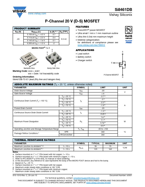
P-Channel 20 V (D-S) MOSFETMarking Code: xxxx = 8461xxx = Date / lot traceability code Ordering Information :Si8461DB-T2-E1 (lead (Pb)-free and halogen-free)FEATURES•TrenchFET ® power MOSFET•Ultra small 1 mm x 1 mm maximum outline •Ultra-thin 0.548 mm maximum height •Material categorization:for definitions of compliance please see /doc?99912APPLICATIONS•Load switch •Battery switch •Charger switchNotesa.Surface mounted on 1" x 1" FR4 board with full copper, t = 10 s.b.Surface mounted on 1" x 1" FR4 board with minimum copper, t = 10 s.c.Refer to IPC/JEDEC ® (J-STD-020), no manual or hand soldering.d.In this document, any reference to case represents the body of the MICRO FOOT device and foot is the bump.e.Based on T A = 25 °C.f.Surface mounted on 1" x 1" FR4 board with full copper.g.Maximum under steady state conditions is 100 °C/W.h.Surface mounted on 1" x 1" FR4 board with minimum copper.i.Maximum under steady state conditions is 190 °C/W.PRODUCT SUMMARYV DS (V)R DS(on) (Ω)I D (A) a, e Q g (TYP.)-200.100 at V GS = -4.5 V-3.79.5 nC0.118 at V GS = -2.5 V -3.40.140 at V GS = -1.8 V -3.10.205 at V GS = -1.5 V-2MICRO FOOT ® 1 x 1Bump S ide View1G4DS 3S 2Back s ide View11m m 1 mm x x x x xx x ABSOLUTE MAXIMUM RATINGS (T A = 25°C, unless otherwise noted)PA AMETE SYMBOL LIMIT UNITDrain-Source Voltage V DS -20VGate-Source VoltageV GS± 8Continuous Drain Current (T J = 150 °C)T A = 25 °CI D -3.7 a A T A = 70 °C -3 a T A = 25 °C -2.5 b T A = 70 °C-1.9 b Pulsed Drain CurrentI DM -20Continuous Source-Drain Diode CurrentT C = 25 °C I S -1.5 a T A = 25 °C -0.65 b Maximum Power DissipationT A = 25 °CP D 1.8 a W T A = 70 °C 1.1 a T A = 25 °C 0.78 b T A = 70 °C0.5 b Operating Junction and Storage Temperature Range T J , T stg -55 to +150°C Package Reflow Conditions cVPR 260IR/Convection260THERMAL RESISTANCE RATINGSPA AMETE SYMBOL TYPICAL MAXIMUM UNITMaximum Junction-to-Ambient f, g t = 10 s R thJA5570°C/WMaximum Junction-to-Ambient h, it = 10 s125160Notesa.Pulse test; pulse width ≤ 300 μs, duty cycle ≤ 2 %.b.Guaranteed by design, not subject to production testing.Stresses beyond those listed under “Absolute Maximum Ratings” may cause permanent damage to the device. These are stress ratings only, and functional operation of the device at these or any other conditions beyond those indicated in the operational sections of the specifications is not implied. Exposure to absolute maximum rating conditions for extended periods may affect device reliability.SPECIFICATIONS (T J = 25°C, unless otherwise noted)PA AMETE R SYMBOL TEST CONDITIONS MIN.TYP.MAX.UNITStaticDrain-Source Breakdown Voltage V DS V GS = 0 V, I D = -250 μA-20--V V DS Temperature Coefficient ΔV DS /T J I D = -250 μA --12-mV/°C V GS(th) Temperature Coefficient ΔV GS(th)/T J - 2.5-Gate-Source Threshold Voltage V GS(th) V DS = V GS , I D = -250 μA -0.4--1V Gate-Source LeakageI GSS V DS = 0 V, V GS = ± 8 V --± 100nA Zero Gate Voltage Drain Current I DSS V DS = -20 V, V GS = 0 V ---1μA V DS = -20 V, V GS = 0 V, T J = 70 °C---10On-State Drain Current aI D(on)V DS ≤ -5 V, V GS = -4.5 V -10--ADrain-Source On-State Resistance aR DS(on)V GS = -4.5 V, I D = -1.5 A-0.0830.100ΩV GS = -2.5 V, I D = -1.5 A -0.0980.118V GS = -1.8 V, I D = -1 A -0.1150.140V GS = -1.5 V, I D = -0.5 A-0.1360.205Forward Transconductance a g fsV DS = -10 V, I D = -1 A-7-S Dynamic bInput Capacitance C iss V DS = -10 V, V GS = 0 V, f = 1 MHz-610-pF Output CapacitanceC oss -120-Reverse Transfer Capacitance C rss -95-Total Gate Charge Q g V DS = -10 V, V GS = -8 V, ID = 1 A -1624nC V DS = -10 V, V GS = -4.5 V, I D = 1 A-9.515Gate-Source Charge Q gs -0.9-Gate-Drain Charge Q gd- 2.6-Gate Resistance R g V GS = -0.1 V, f = 1 MHz - 6.5-ΩTurn-On Delay Time t d(on)V DD = -10 V, R L = 10 ΩI D ≅ -1 A, V GEN = -4.5 V, R g = 1 Ω-1525ns Rise Timet r-2540Turn-Off Delay Time t d(off) -3555Fall Timet f -1015Turn-On Delay Time t d(on)V DD = -10 V, R L = 10 ΩI D ≅ -1 A, V GEN = -8 V, R g = 1 Ω-715Rise Timet r -1220Turn-Off Delay Time t d(off) -3250Fall Timet f -1220Drain-Source Body Diode Characteristics Continuous Source-Drain DiodeCurrentI S T A = 25 °C---1.5APulse Diode Forward Current I SM ---20Body Diode VoltageV SD I S = -1 A, V GS = 0 V--0.8-1.2V Body Diode Reverse Recovery Time t rr I F = -1 A, dI/dt = 100 A/μs, T J = 25 °C-1530ns Body Diode Reverse Recovery Charge Q rr -1020nC Reverse Recovery Fall Time t a -9-ns Reverse Recovery Rise Timet b-6-On-Resistance vs. Drain Current and Gate VoltageGate ChargeTransfer CharacteristicsCapacitanceOn-Resistance vs. Junction TemperatureTYPICAL CHARACTERISTICSThreshold VoltageSingle Pulse Power, Junction-to-Ambient Safe Operating Area, Junction-to-AmbientTYPICAL CHARACTERISTICS (25 °C, unless otherwise noted)Current Derating aPower DeratingNote•When mounted on 1" x 1" FR4 with full copper.Notea.The power dissipation P D is based on T J (max.) = 150 °C, using junction-to-case thermal resistance, and is more useful in settling the upper dissipation limit for cases where additional heatsinking is used. It is used to determine the current rating, when this rating falls below the package limit.TYPICAL CHARACTERISTICS (25 °C, unless otherwise noted)Normalized Thermal Transient Impedance, Junction-to-Ambient (1" x 1" FR4 Board with Full Copper)Vishay Silico nix maintains wo rldwide manufacturing capability. Pro ducts may be manufactured at o ne o f several qualified lo catio ns. Reliability data fo r Silico n Technology and Package Reliability represent a composite of all qualified locations. For related documents such as package/tape drawings, part marking, and reliability data, see /ppg?65001.Package InformationVishay SiliconixMICRO FOOT ®: 4-Bumps(1 mm x 1 mm, 0.5 mm Pitch, 0.286 mm Bump Height)Notes1.Bumps are 95.5/3.8/0.7 Sn/Ag/Cu.2.Backside surface is coated with a Ti/Ni/Ag layer.3.Non-solder mask defined copper landing pad.ser mark on the backside surface of die.5.“b1” is the diameter of the solderable substrate surface, defined by an opening in the solder resist layer solder mask defined.6.• is the location of pin 1Note•Use millimeters as the primary measurement.DIM. MILLIMETERSINCHES MIN. NOM.MAX. MIN. NOM.MAX. A 0.4580.5040.5500.01800.01980.0217A10.2140.2500.2860.00840.00980.0113A20.2440.2540.2640.00960.01000.0104b 0.2970.3300.3630.01170.01300.0143b10.2500.0098e 0.5000.0197s 0.2100.2300.2500.00830.00910.0096D 0.9200.960 1.0000.03620.03780.0394K0.0290.0650.1020.00110.00260.0040ECN: T15-0176-Rev. A, 27-Apr-15DWG: 6039Legal Disclaimer Notice VishayDisclaimerALL PRODUCT, PRODUCT SPECIFICAT IONS AND DAT A ARE SUBJECT T O CHANGE WIT HOUT NOT ICE T O IMPROVE RELIABILITY, FUNCTION OR DESIGN OR OTHERWISE.Vishay Intertechnology, Inc., its affiliates, agents, and employees, and all persons acting on its or their behalf (collectively, “Vishay”), disclaim any and all liability for any errors, inaccuracies or incompleteness contained in any datasheet or in any other disclosure relating to any product.Vishay makes no warranty, representation or guarantee regarding the suitability of the products for any particular purpose or the continuing production of any product. To the maximum extent permitted by applicable law, Vishay disclaims (i) any and all liability arising out of the application or use of any product, (ii) any and all liability, including without limitation special, consequential or incidental damages, and (iii) any and all implied warranties, including warranties of fitness for particular purpose, non-infringement and merchantability.Statements regarding the suitability of products for certain types of applications are based on Vishay’s knowledge of typical requirements that are often placed on Vishay products in generic applications. Such statements are not binding statements about the suitability of products for a particular application. It is the customer’s responsibility to validate that a particular product with the properties described in the product specification is suitable for use in a particular application. Parameters provided in datasheets and / or specifications may vary in different applications and performance may vary over time. All operating parameters, including typical parameters, must be validated for each customer application by the customer’s technical experts. Product specifications do not expand or otherwise modify Vishay’s terms and conditions of purchase, including but not limited to the warranty expressed therein.Except as expressly indicated in writing, Vishay products are not designed for use in medical, life-saving, or life-sustaining applications or for any other application in which the failure of the Vishay product could result in personal injury or death. Customers using or selling Vishay products not expressly indicated for use in such applications do so at their own risk. Please contact authorized Vishay personnel to obtain written terms and conditions regarding products designed for such applications.No license, express or implied, by estoppel or otherwise, to any intellectual property rights is granted by this document or by any conduct of Vishay. Product names and markings noted herein may be trademarks of their respective owners.© 2017 VISHAY INTERTECHNOLOGY, INC. ALL RIGHTS RESERVED。
SI8421中文资料

Applications
Isolated switch mode supplies Isolated ADC, DAC
Motor control Power factor correction systems
Safety Regulatory Approvals
UL recognition:2500 Vrms for 1 Minute per UL1577 CSA component acceptance notice
—
9
12
Si8421-A,-B,-C, VDD2
All inputs 0 DC
—
9
12
Si8421-A,-B,-C, VDD1
All inputs 1 DC
—
10
14
Si8421-A,-B,-C, VDD2
All inputs 1 DC
—
10
14
10 Mbps Supply Current (All inputs = 5 MHz square wave, CI = 15 pF on all outputs)
3.1. Theory of Operation . . . . . . . . . . . . . . . . . . . . . . . . . . . . . . . . . . . . . . . . . . . . . . . . . 19 3.2. Eye Diagram . . . . . . . . . . . . . . . . . . . . . . . . . . . . . . . . . . . . . . . . . . . . . . . . . . . . . . . 19 4. Layout Recommendations . . . . . . . . . . . . . . . . . . . . . . . . . . . . . . . . . . . . . . . . . . . . . . . . 20 4.1. Supply Bypass . . . . . . . . . . . . . . . . . . . . . . . . . . . . . . . . . . . . . . . . . . . . . . . . . . . . . 20 4.2. Input and Output Characteristics . . . . . . . . . . . . . . . . . . . . . . . . . . . . . . . . . . . . . . . . 21 4.3. RF Radiated Emissions . . . . . . . . . . . . . . . . . . . . . . . . . . . . . . . . . . . . . . . . . . . . . . . 21 4.4. RF Immunity and Common Mode Transient Immunity . . . . . . . . . . . . . . . . . . . . . . . 22 5. Pin Descriptions . . . . . . . . . . . . . . . . . . . . . . . . . . . . . . . . . . . . . . . . . . . . . . . . . . . . . . . . . 23 6. Ordering Guide . . . . . . . . . . . . . . . . . . . . . . . . . . . . . . . . . . . . . . . . . . . . . . . . . . . . . . . . . . 24 7. Package Outline: 8-Pin SOIC . . . . . . . . . . . . . . . . . . . . . . . . . . . . . . . . . . . . . . . . . . . . . . . 25 Contact Information . . . . . . . . . . . . . . . . . . . . . . . . . . . . . . . . . . . . . . . . . . . . . . . . . . . . . . . .26
MAS9181BN资料

The MAS9181 comprises eight digital to analog converters (DACs) each controlled by a two-wire I2C bus. The DACs are individually programmed using an 8-bit word to select an output from one of 256 voltage steps. The maximum output voltage of all DACs is set by Vmax and the resolution is Vmax/256. At power-on all outputs are set to their lowest value. The I2C-bus slave receiver has 3 programmable address pins (2 forMAS9181 CS).· Rail to rail output stages· Octal 8-bit DACs on a single monolithic chip · Power supply range from +5 V to +12 V · -20°C to +85°C temperature range· 16-pin PDIL and SO package· Power-up reset · Trimmer replacement· AGC/AFT or TVs and VCRs · Graphic equalizers· High resolution monitorsVDD 11P Positive supply voltageVmax 22I Control input for DAC maximum output voltage SDA 33I/O I 2C bus serial data input/output SCL 44I I 2C bus serial data clockA 056I Programmable address bits for I 2C bus slave receiver A 167I Programmable address bits for I 2C bus slave receiver A 27NC I Programmable address bits for I 2C bus slave receiver GND 88G GroundDAC099O Analog voltage output DAC11010O Analog voltage output DAC21111O Analog voltage output DAC31212O Analog voltage output DAC41313O Analog voltage output DAC51414O Analog voltage output DAC61515O Analog voltage output DAC71616OAnalog voltage output*1 MAS9181BN (PDIP16)*2 MAS9181CS (SO16)(conditions)Supply Voltage VDD -0.518VSupply current IDD -1040 I 2C-bus line voltage V(3),V(4)-0.5 5.9V Input voltage Vin -0.5VDD+0.5VOutput voltageVo -0.5VDD+0.5Maximum current on any pinImax 10mA total power dissipation Ptot 500mWOperating ambient temperature range Tamb -20+85oC Storage temperature rangeTstg-65+150oCoCSupply Voltage VDD 4.51213.2V Supply current IDD No loads, Vmax=VDD=12V, Alldata=00OCT 3.0 5.0mA Total power dissipationPtotNo loads, Vmax=VDD=12V, Alldata=00OCT4060mW(All voltages are with respect to GND; Tamb = -20 o C to 85 o C; VDD = 5V to 12V unless otherwise specified)Input voltage rangeV I -0.5 5.5V Input low voltage V IL 1.0V Input high voltage V IH 3.0VInput leakage currentI ILVin = 0V or VDD-1+1元器件交易网(All voltages are with respect to GND; Tamb = -20 o C to 85 o C; VDD = 5V to 12V unless otherwise specified)Input voltage range V I 0VDD V Input low voltage V IL 1.0V Input high voltage V IH 3.0VInput current lowI IL-10-15A(All voltages are with respect to GND; Tamb = -20 o C to 85 o C; VDD = 5V to 12V unless otherwise specified)Pin 2 current I 2710A 0.1VDD-0.1VDAC output (pin 9 to 16)Output voltage rangeVoIo = +/- 500DAC output drive range Io Upper side saturation voltage= 0.2v Low side saturation voltage = 0.2v-11mA Output capacitive loadCo2nF(All voltages are with respect to GND; Tamb = -20 o C to 85 o C; VDD = 5V to 12V unless otherwise specified)Output voltage lowV OL I 3 = 3.0 mA 0.4V(All voltages are with respect to GND; Tamb = -20 o C to 85 o C; VDD = 5V to 12V unless otherwise specified)Differential nonlinearity DNL Io = 0 (without load)Vmax = VDD-1.0-11LSB Integral nonlinearity INL Io = 0 (without load)Vmax = VDD-1.0-1.51.5LSB Zero code error1ZCE data = 001030mV Power supply rejection1PSRR 5mV/VZero code temperature coefficient 1TCo-200200元器件交易网The MAS9181 I 2C-bus interface is a receiver- only slave. Data is accepted from the I 2C - bus in the following format.S0 1 0 0 A2 A1 A0 0AI3 I2 I1 I0 SD SC SBSAAD7 D6 D5 D4 D3 D2 D1D0APAddress byteInstruction byteFirst data byteS Start condition A2, A1, A0programmable address bits P Stop condition I3, I2, I1, I0instruction bits AAcknowledgementSD, SC, SB, SAsub-address bits D7, D6, D5, D4, D3, D2, D2, D1, D0data bitsSDASCLBit Transfer on the I C-busData line stable (data valid)Change of data allowedSP1-7891-7891-789Start conditionStop conditionSDASCLAddressDataDataR/WAckAckAckComplete Data TransferValid addresses are 40, 42, 44, 46, 48, 4A, 4C, 4E(hex), depending on the programming of bits A2, A1 and A0. With these addresses, up to eight MAS9181 ICs can be operated independently from one I2C-bus. No other addresses are acknowledged by the MAS9181. The address inputs A0, A1 and A2 are programmed by connection to GND for An = 0 or to VDD for An = 1. If the inputs are left floating, An = 1 will result. For MAS9181CS, A2 is always 1.Valid instructions from 00 to 0F and F0 to FF (hex); MAS9181 will not respond to other instruction value, but will still generate an acknowledgement. Instructions 00 to0F cause auto-incrementing of the sub-address (bits SD to SA) when more than one data byte is sent within one transmission. With auto-incrementing, the first data byte is written into the DAC addessed by bits SD to SA and then the sub-address is automatically incremented by one position for the next databyte in the series. Auto-incrementing does not occur with instructions F0 to FF. The DAC addressed by the sub-address will always receive the data if more than one data byte is sent. Valid sub-addresses (bits SD to SA) are 0 to 7 (hex) relating numerically to DAC0 to DAC7. When the auto-incrementing function is used, the sub-address will sequence through all possible values (0 to F, 0 to F, etc.). While the sub-address is between 8 and F no DAC outputs change.Input SCL (pin 4) and input/output SDA (pin 3) conform to I2C-bus specifications. Pins 3 and 4 are protected against voltage pulses by internal zener diodes connected to the ground plane and therefore the normal bus line voltage shall not exceed 5.5V.Input Vmax (pin 2) provides a means of comprising the output voltage swing of the DACs. The maximum DAC output voltage is restricted to approximately Vmax while the 8-bit resolution is maintained, therefore giving a finer voltage resolution of smaller output swings.ClockData+12v+12v100nF100nF+5v5k5k MAS9181DAC7DAC0DAC1DAC2DAC3DAC4DAC5DAC6161514131211109VDDGNDA2A1SCL SDAA076543Micro Controller1.120.102.360.302.64PLANESEATING 5° TYP.10.4910.1110.64PIN 110.017.597.391.27TYP.0.360.480.945°TYP0.33 x 45°0.86 T Y P.16 LEAD SO OUTLINE (300 MIL BODY)ALL MEASUREMENTS IN mm0-0.13RAD.5° TYP.5° TYP.5° TYP.0.25 RAD.MIN.1 PIN18.9321.336.107.117.62BSC5-7°5.52.935.334.95M A X0.254BSC2.540.360.56 1.771.15PLANESEATING 0.63 TYPICAL1.5216 LEAD PDIP OUTLINE (300 MIL BODY)MAS9181BN OCTAL 8-BIT TRIMMER-IC16 Pin PDIP 0.3"MAS9181CS OCTAL 8-BIT TRIMMER-IC16 Pin SO 0.3" 2 Address PinsMicro Analog Systems Oy Kamreerintie 2, P.O.Box 51 FIN-02771 ESPOO, FINLAND Tel. (09) 80 521Tel. Int. +358 9 80 521 Telefax +358 9 805 3213 E-mail: i nfo@NOTICEMicro Analog Systems Oy reserves the right to make changes to the products contained in this data sheet in order to improve the design or performance and to supply the best possible products. Micro Analog Systems Oy assumes no responsibility for the use of any circuits shown in this data sheet, conveys no license under any patent or other rights unless otherwise specified in this data sheet, and makes no claim that circuits are free from patent infringement. Applications for any devices shown in this data sheet are for illustration only and Micro Analog Systems Oy makes no claim or warranty that such applications will be suitable for the use specified without further testing or modification.。
SI8420-B-IS中文资料

Preliminary Rev. 0.1
3
元器件交易网
Si8410/20/21
1. Electrical Specifications
Table 1. Electrical Characteristics
(VDD1 = 5 V, VDD2 = 5 V, TA = –40 to 125 ºC)
—
7
10
Si8420-A,-B,-C, VDD2
All inputs 0 DC
—
4
7
Si8420-A,-B,-C, VDD1
All inputs 1 DC
—
11
15
Si8420-A,-B,-C, VDD2
All inputs 1 DC
—
4
6
Si8421-A,-B,-C, VDD1
All inputs 0 DC
>25 kV/µs DC correct No start-up initialization required <10 µs Startup Time High temperature operation
125 °C at 100 Mbps 100 °C at 150 Mbps Narrow body SOIC-8 package
元器件交易网
Si8410/20/21
2
Preliminary Rev. 0.1
元器件交易网
TABLE OF CONTENTS
Si8410/20/21
Section
Page
1. Electrical Specifications . . . . . . . . . . . . . . . . . . . . . . . . . . . . . . . . . . . . . . . . . . . . . . . . . . .4 2. Typical Performance Characteristics . . . . . . . . . . . . . . . . . . . . . . . . . . . . . . . . . . . . . . . . 17 3. Application Information . . . . . . . . . . . . . . . . . . . . . . . . . . . . . . . . . . . . . . . . . . . . . . . . . . . 19
AO4918中文资料

Symbol V DS I FM T J , T STGMaximum SchottkyUnits30V T A =25°CParameterReverse VoltageA2.2203T A =70°C Pulsed Diode Forward Current BContinuous Forward Current AP D I F T A =25°C T A =70°CJunction and Storage Temperature RangePower Dissipation AW 1.28-55 to 150°C2AO4918AO4918Symbol Units R θJL Symbol Units R θJLR θJLTHIS PRODUCT HAS BEEN DESIGNED AND QUALIFIED FOR THE CONSUMER MARKET. APPLICATIONS OR USES AS CRITICAL COMPONENTS IN LIFE SUPPORT DEVICES OR SYSTEMS ARE NOT AUTHORIZED. AOS DOES NOT ASSUME ANY LIABILITY ARISING OUT OF SUCH APPLICATIONS OR USES OF ITS PRODUCTS. AOS RESERVES THE RIGHT TO IMPROVE PRODUCT DESIGN,FUNCTIONS AND RELIABILITY WITHOUT NOTICE.Maximum Junction-to-Lead CSteady-State8626.650.4R θJA 62.5Maximum Junction-to-AmbientAt ≤ 10s R θJA Maximum Junction-to-Ambient ASteady-State 110110Maximum Junction-to-Lead CSteady-State 30.5Typ Maximum Junction-to-AmbientASteady-State Parameter: Thermal Characteristics MOSFET Q1Maximum Junction-to-AmbientAt ≤ 10s 40Thermal Characteristics Schottky62.5405381.962.5°C/WMaximum Junction-to-AmbientASteady-State Max °C/W°C/WParameter: Thermal Characteristics MOSFET Q2Typ Max Maximum Junction-to-AmbientAt ≤ 10s R θJA 5381.9110Maximum Junction-to-Lead CSteady-State 30.540A: The value of R θJA is measured with the device mounted on 1in 2 FR-4 board with 2oz. Copper, in a still air environment with T A =25°C. The value in any given application depends on the user's specific board design. The current rating is based on the t ≤ 10s thermal resistance rating.B: Repetitive rating, pulse width limited by junction temperature.C. The R θJA is the sum of the thermal impedence from junction to lead R θJL and lead to ambient.D. The static characteristics in Figures 1 to 6 are obtained using 80 µs pulses, duty cycle 0.5% max.E. These tests are performed with the device mounted on 1 in 2 FR-4 board with 2oz. Copper, in a still air environment with T A =25°C. The SOA curve provides a single pulse rating.F. The Schottky appears in parallel with the MOSFET body diode, even though it is a separate chip. Therefore, we provide the net forward drop, capacitance and recovery characteristics of the MOSFET and Schottky. However, the thermal resistance is specified for each chip separately. Rev4: August 2005AO4918SymbolMin TypMax UnitsBV DSS 30V0.0070.053.2101220I GSS 100nA V GS(th)0.6 1.12V I D(ON)40A 11.714.5T J =125°C15.41913.116m Ωg FS 3037S V SD 0.460.5V I S3.5A C iss 37404488pF C oss 295pF C rss 186pF R g0.86 1.1ΩQ g 30.537nC Q gs 4.5nC Q gd 8.5nC t D(on)69ns t r 8.212ns t D(off)54.575ns t f 10.515ns t rr Body Diode + Schottky Reverse Recovery Time I F =9.3A, dI/dt=100A/µs 23.528ns Q rrBody Diode + Schottky Reverse Recovery ChargeI F =9.3A, dI/dt=100A/µs13.316nCTHIS PRODUCT HAS BEEN DESIGNED AND QUALIFIED FOR THE CONSUMER MARKET. APPLICATIONS OR USES AS CRITICAL COMPONENTS IN LIFE SUPPORT DEVICES OR SYSTEMS ARE NOT AUTHORIZED. AOS DOES NOT ASSUME ANY LIABILITY ARISING OUT OF SUCH APPLICATIONS OR USES OF ITS PRODUCTS. AOS RESERVES THE RIGHT TO IMPROVE PRODUCT DESIGN,FUNCTIONS AND RELIABILITY WITHOUT NOTICE.Gate Source Charge Gate Drain Charge Turn-On DelayTime V GS =10V, V DS =15V, R L =1.6Ω, R GEN =3ΩV GS =4.5V, V DS =15V, I D =9.3ATurn-On Rise Time Turn-Off DelayTime Turn-Off Fall TimeSWITCHING PARAMETERS Total Gate Charge Gate resistanceV GS =0V, V DS =0V, f=1MHzForward TransconductanceV DS =5V, I D =9.3ADiode+Schottky Forward Voltage I S =1A Maximum Body-Diode+Schottky Continuous CurrentDYNAMIC PARAMETERS Input Capacitance V GS =0V, V DS =15V, f=1MHz Output Capacitance (FET + Schottky)Reverse Transfer Capacitance R DS(ON)Static Drain-Source On-ResistanceV GS =10V, I D =9.3Am ΩV GS =4.5V, I D =8.8AGate Threshold Voltage V DS =V GS I D =250µA On state drain currentV GS =4.5V, V DS =5V mA Gate-Body leakage current V DS =0V, V GS = ±12V V R =30V, T J =125°C V R =30V, T J =150°C Drain-Source Breakdown Voltage I D =250µA, V GS =0V I DSS Zero Gate Voltage Drain Current.(Set by Schottky leakage)V R =30VQ1 Electrical Characteristics (T J =25°C unless otherwise noted)ParameterConditions STATIC PARAMETERS A: The value of R θJA is measured with the device mounted on 1in 2 FR-4 board with 2oz. Copper, in a still air environment with T A =25°C. The value in any given application depends on the user's specific board design. The current rating is based on the t ≤ 10s thermal resistance rating.B: Repetitive rating, pulse width limited by junction temperature.C. The R θJA is the sum of the thermal impedence from junction to lead R θJL and lead to ambient.D. The static characteristics in Figures 1 to 6,12,14 are obtained using 80 µs pulses, duty cycle 0.5% max.E. These tests are performed with the device mounted on 1 in 2 FR-4 board with 2oz. Copper, in a still air environment with T A =25°C. The SOA curve provides a single pulse rating.F. The Schottky appears in parallel with the MOSFET body diode, even though it is a separate chip. Therefore, we provide the net forward drop, capacitance and recovery characteristics of the MOSFET and Schottky. However, the thermal resistance is specified for each chip separately Rev4: August 2005.AO4918Q1 TYPICAL ELECTRICAL AND THERMAL CHARACTERISTICSAO4918AO4918SymbolMin TypMax UnitsBV DSS 30V 0.0041T J =55°C5I GSS 100nA V GS(th)1 1.83V I D(ON)30A 14.918T J =125°C222721.627m Ωg FS 23S V SD 0.450.5V I S3A C iss 10401250pF C oss 180pF C rss 110pF R g0.70.85ΩQ g (10V)19.224nC Q g 9.3612nC Q gs 2.6nC Q gd 4.2nC t D(on) 5.27.5ns t r 4.4 6.5ns t D(off)17.325ns t f 3.35ns t rr Body Diode Reverse Recovery TimeI F =8.5A, dI/dt=100A/µs16.721ns Q rrBody Diode Reverse Recovery Charge I F =8.5A, dI/dt=100A/µs6.710nCTHIS PRODUCT HAS BEEN DESIGNED AND QUALIFIED FOR THE CONSUMER MARKET. APPLICATIONS OR USES AS CRITICAL COMPONENTS IN LIFE SUPPORT DEVICES OR SYSTEMS ARE NOT AUTHORIZED. AOS DOES NOT ASSUME ANY LIABILITY ARISIN OUT OF SUCH APPLICATIONS OR USES OF ITS PRODUCTS. AOS RESERVES THE RIGHT TO IMPROVE PRODUCT DESIGN,FUNCTIONS AND RELIABILITY WITHOUT NOTICE.V GS =10V, V DS =15V, I D =8.3ATotal Gate Charge Turn-On Rise Time Turn-Off DelayTime Turn-Off Fall TimeReverse Transfer Capacitance SWITCHING PARAMETERS Total Gate Charge Gate Source Charge Gate Drain Charge Turn-On DelayTime V GS =10V, V DS =15V, R L =1.8Ω, R GEN =3ΩGate resistanceV GS =0V, V DS =0V, f=1MHzForward TransconductanceV DS =5V, I D =8.3ADiode+Schottky Forward Voltage I S =1AMaximum Body-Diode+Schottky Continuous CurrentDYNAMIC PARAMETERS Input Capacitance V GS =0V, V DS =15V, f=1MHz Output Capacitance R DS(ON)Static Drain-Source On-ResistanceV GS =10V, I D =8.3Am ΩV GS =4.5V, I D =7AGate Threshold Voltage V DS =V GS I D =250µA On state drain currentV GS =4.5V, V DS =5V µA Gate-Body leakage current V DS =0V, V GS = ±20V Drain-Source Breakdown Voltage I D =250µA, V GS =0V I DSS Zero Gate Voltage Drain Current V DS =24V, V GS =0VQ2 Electrical Characteristics (T J =25°C unless otherwise noted)ParameterConditions STATIC PARAMETERS A: The value of R θJA is measured with the device mounted on 1in 2 FR-4 board with 2oz. Copper, in a still air environment with T A =25°C. The value in any given application depends on the user's specific board design. The current rating is based on the t ≤ 10s thermal resistance rating.B: Repetitive rating, pulse width limited by junction temperature.C. The R θJA is the sum of the thermal impedence from junction to lead R θJL and lead to ambient.D. The static characteristics in Figures 1 to 6,12,14 are obtained using 80 µs pulses, duty cycle 0.5% max.E. These tests are performed with the device mounted on 1 in 2FR-4 board with 2oz. Copper, in a still air environment with T A =25°C. The SOA curve provides a single pulse rating. Rev4: August 2005AO4918Q2 Electrical Characteristics (T J=25°C unless otherwise noted)AO4918。
918D系列模型电机数据手册说明书

REDUCTION TABLE. R.P.M.This miniature gearbox is of steel and brass construction with brass gears and is mounted on a 1mm thickness steel bracket. It incorporatesa high quality three pole motor with sleeved bearings. The design and construction of the unit make it suitable for a host of model and light industrial applications.918D SERIES 25mm SINGLE RATIO METAL GEARBOXRATIOS NOW AVAILABLE AS EX-STOCK ITEMS.918D151(1.5v - 3v) WITH RE 280 MOTOR (RATIO 15:1). 2mm SHAFT918D15112 (12v - 24v) WITH RE 280/1 MOTOR (RATIO 15:1). 2mm SHAFT 918D151/1(1.5v - 3v) WITH RE 280 MOTOR (RATIO 15:1). 4mm SHAFT918D15112/1 (12v - 24v) WITH RE 280/1 MOTOR (RATIO 15:1). 4mm SHAFT 918D301/1(1.5v - 3v) WITH RE 280 MOTOR (RATIO 30:1). 4mm SHAFT918D30112/1 (12v - 24v) WITH RE 280/1 MOTOR (RATIO 30:1). 4mm SHAFT 918D1001/1 (1.5v - 3v) WITH RE 280 MOTOR (RATIO 100:1). 4mm SHAFT918D100112/1 (12v - 24v) WITH RE 280/1 MOTOR (RATIO 100:1). 4mm SHAFT 918D2501/1 (1.5v - 3v) WITH RE 280 MOTOR (RATIO 250:1). 4mm SHAFT 918D250112/1 (12v - 24V) WITH RE280/1 MOTOR (RATIO 250:1). 4mm SHAFT 918D3601/1 (1.5v - 3v) WITH RE280/3 MOTOR (RATIO 360:1). 4mm SHAFT 918D360112/1 (12v - 24v) WITH RE280/4 MOTOR (RATIO 360:1). 4mm SHAFT 918D5001/1 (1.5v - 3v) WITH RE280 MOTOR (RATIO 500:1). 4mm SHAFT 918D500112/1 (12v - 24v) WITH RE280 MOTOR (RATIO 500:1). 4mm SHAFT918D10241/1 (12v - 24v) WITH RE280/1 MOTOR (RATIO 1024:1). 4mm SHAFTIMPORTANT NOTICEDue to the wide range ofapplications for thisproduct it is the usersresponsibility to estab-lish the products suit-ability for their indi-vidual purpose(s).WITH 2mm OUTPUT SHAFT (15:1 ONLY)WITH 4mm OUTPUT SHAFT (ALL RATIOS)FELDERLAND LANE. WORTH. DEAL. KENTStall Current RE280 at 1.5v = 2.41ANote: Motor speeds may vary by (+) or (-) 12.5%IMPORTANT NOTICEAt very low ratios the torque produced by this geared motorcombination may exceed the maximum permissible torque ofthe gearbox. In this situation the unit must not be allowed tostall as this may damage the gears. Please refer to the table ofthe gearbox ratings to ascertain the appropriate geared motorcombination.GEARBOX DIMENSIONS.Subject to minimum order quantities of 250 units, the following ratios are also available with a six week lead-time.The physical dimensions of these other gearboxes may vary from the data as illustrated above. Details of individual gearboxes are available upon request.GEARBOX 6:1 with RE280 motor (1.5v - 3v)GEARBOX 6:1with RE280/1 motor (12v - 24v)GEARBOX 10:1 with RE280 motor (1.5v - 3v)GEARBOX 10:1with RE280/1 motor (12v - 24v)GEARBOX 21:1 with RE280 motor (1.5v - 3v)GEARBOX 21:1with RE280/1 motor (12v - 24v)GEARBOX 44:1 with RE280 motor (1.5v - 3v)GEARBOX 44:1with RE280/1 motor (12v - 24v)GEARBOX 60:1 with RE280 motor (1.5v - 3v)GEARBOX 60:1with RE280/1 motor (12v - 24v)GEARBOX 77:1 with RE280 motor (1.5v - 3v)GEARBOX 77:1with RE280/1 motor (12v - 24v)GEARBOX 112:1 with RE280 motor (1.5v - 3v)GEARBOX 112:1with RE280/1 motor (12v - 24v)GEARBOX 150:1 with RE280 motor (1.5v - 3v)GEARBOX 150:1with RE280/1 motor (12v - 24v)GEARBOX 170:1 with RE280 motor (1.5v - 3v)GEARBOX 170:1with RE280/1 motor (12v - 24v)GEARBOX 200:1 with RE280 motor (1.5v - 3v)GEARBOX 200:1with RE280/1 motor (12v - 24v)GEARBOX 250:1 with RE280 motor (1.5v - 3v)GEARBOX 250:1with RE280/1 motor (12v - 24v)GEARBOX 320:1 with RE280 motor (1.5v - 3v)GEARBOX 320:1with RE280/1 motor (12v - 24v)GEARBOX 360:1 with RE280 motor (1.5v - 3v)GEARBOX 360:1with RE280/1 motor (12v - 24v)GEARBOX 400:1 with RE280 motor (1.5v - 3V)GEARBOX 400:1with RE280/1 motor (12v - 24v)GEARBOX 500:1 with RE280 motor (1.5v - 3v)GEARBOX 500:1with RE280/1 motor (12v - 24v)GEARBOX 700:1 with RE280 motor (1.5v - 3v)GEARBOX 700:1with RE280/1 motor (12v - 24v)GEARBOX 800:1 with RE280 motor (1.5v - 3v)GEARBOX 800:1with RE280/1 motor (12v - 24v)GEARBOX 900:1 with RE280 motor (1.5v - 3v)GEARBOX 900:1with RE280/1 motor (12v - 24v)GEARBOX 1153:1 with RE280 motor (1.5v - 3v)GEARBOX 1153:1with RE280/1 motor (12v - 24v)Part No. 917D9. Voltage Regulator. (6-15v DC Input, 3v, 1.5amp output)Part No. 917D10. Voltage Regulator.(6-15v DC Input. 1.5v, 1.5amp output)Part No. 917D11. Voltage Regulator.(6-15v DC Input. 4.5v, 1.5amp output)ACCESSORIES FOR 918D SERIES GEARBOX.Part No. 917D2458. Pinions (Plastic) 12 tooth. 1.9mm I.D.Part No. 917D2515. "O"Ring 70mm x 5mm Dia.Part No. 918D3. Pulley. 2mm I.D.(16mm dia. x 13.6mm) (Aluminium)Part No. 918D3/1. Pulley 4mm I.D.(16mm dia x 13.6mm( (Aluminium)Part No. 918D2. Pulley. 2mm I.D.(25mm dia. x 14.75mm) (Aluminium)Part No. 918D2/1. Pulley 4mm I.D.(25mm dia. x 14.75mm) (Aluminium)Part No. 918D1. In-Line Coupling.2mm - 3mm. (Dia. 8mm x 18.4mm)Part No. 918D1/1. In-Line Coupling4mm - 4mm. (Dia. 8mm x 18.4mm)Part No. 918D4. Gear Adapter.2mm I.D. Shaft Dia 6mm.Part No. 918D4/1 Gear Adapter.4mm I.D. Shaft Dia 6mm.(Above for 280 motor only)Part No. 918D7. Nylon Bevel Gears (1:1). O.D. 17.2mm.4mm I.D.Part No. 1071. Anti vibrationmount. M3Part No. 918D8.Stainless Steel Shaft.4mm OD x 150mm Part No. 1105/61Universal Coupling. 4mm - 4mm67(69 on 1024:1 ratio)FELDERLAND LANE. WORTH. DEAL. KENT. CT14 OBT TEL: 01304 612132.E-MAIL:*******************THE ABOVE FIGURES ARE A GUIDE ONLY AND DO NOT FORM ANY CONTRACTUAL OBLIGATION ON THE PART OF MFA/COMO DRILLS.4.08.02.08.03.56.514.5Part No. 918D10.Bearing Blocks. 4mm I.D.(20 x 20 x 12.5mm)。
SI9121DY-3资料

Si9121 Vishay SiliconixDocument Number: 71112 S-40708—Rev. C, 1High-Voltage, Non-Isolated Buck-Boost Converterfor ISDN Digital PhonesFEATURESD Fixed +5-V or +3.3-V OutputD Integrated Floating Feedback Amplifier D On-Chip 70-V, 1.5-W N-Channel MOSFET SwitchD Integrated High Voltage Start-Up Circuit, with V CC Regulator D−10-V to −60-V Input Voltage RangeD95-kHz PWM OperationD Integrated Soft-Start and OscillatorD High Efficiency Over Full Load RangeD Under Voltage LockoutD Current Mode ControlD Hiccup Mode Short CircuitProtectionD Thermal ShutdownD SOIC-8 Narrow-Body PackageDESCRIPTIONThe Si9121 simplifies the −48-V to +5-V or +3.3-V converter design for ISDN application by integrating the floating feedback error amplifier providing direct output voltage regulation. This approach eliminates the need for an external shunt regulator. The Si9121 also integrates a high voltage depletion mode MOSFET which allows the converter to be powered directly from the high input bus voltage without requiring an external start-up circuit. Combined with simple magnetic design due to its non-isolated topology, the Si9121 provides a one-chip solution for complete ISDN power supply.In order to reduce external component count, the Si9121 has a fully integrated 95-kHz oscillator and soft-start circuit.The Si9121 is available in both standard and lead (Pb)-free SOIC-8 pin packages, and is offered in either +5-V or +3.3-V fixed output options (Si9121DY-5 or Si9121DY-3, respectively). In order to satisfy the stringent ambient temperature requirements in many applications, the Si9121 is rated to the industrial temperature range of −40_C to 85_C.FUNCTIONAL BLOCK DIAGRAMV NEG −48 V V OUT+5 V/400 mA or+3.3 V/400 mASi9121Vishay Siliconix2Document Number: 71112S-40708—Rev. C, 19-Apr-04ABSOLUTE MAXIMUM RATINGS (ALL VOLTAGES REFERENCED TO GND = 0 V)V NEG −63 V . . . . . . . . . . . . . . . . . . . . . . . . . . . . . . . . . . . . . . . . . . . . . . . . . . . . . . V CS V NEG −0.3 V to V CC + 0.3 V . . . . . . . . . . . . . . . . . . . . . . . . . . . . . . . . . . . . . V CC V NEG + 13.2 V . . . . . . . . . . . . . . . . . . . . . . . . . . . . . . . . . . . . . . . . . . . . . . . . I LX (peak current ) 3 A . . . . . . . . . . . . . . . . . . . . . . . . . . . . . . . . . . . . . . . . . . . . . V OUT 6 V . . . . . . . . . . . . . . . . . . . . . . . . . . . . . . . . . . . . . . . . . . . . . . . . . . . . . . . . Bypass, CS V NEG −0.3 V to V CC +0.3 V . . . . . . . . . . . . . . . . . . . . . . . . . . . . . . (V LX − V CS ) internal power MOSFET 70 V . . . . . . . . . . . . . . . . . . . . . . . . . . . . Storage Temperature −65 to 150_C. . . . . . . . . . . . . . . . . . . . . . . . . . . . . . . . . . Operating Junction Temperature 150_C . . . . . . . . . . . . . . . . . . . . . . . . . . . . . . Power Dissipation (Package)a8-Pin SOIC (Y Suffix)b 1.25 W . . . . . . . . . . . . . . . . . . . . . . . . . . . . . . . . . . . . . . Thermal Impedance (Q JA )a8-Pin SOIC 100 _C/W . . . . . . . . . . . . . . . . . . . . . . . . . . . . . . . . . . . . . . . . . . . . . Notesa.Device mounted with all leads soldered or welded to PC board.b.Derate 10 mW/_C above 25_C.Stresses beyond those listed under “Absolute Maximum Ratings” may cause permanent damage to the device. These are stress ratings only, and functional operation of the device at these or any other conditions beyond those indicated in the operational sections of the specifications is not implied. Exposure to absolute maximum rating conditions for extended periods may affect device reliability.RECOMMENDED OPERATING RANGE (ALL VOLTAGES REFERENCED TO GND = 0 V)V NEG −10 V to −60 V . . . . . . . . . . . . . . . . . . . . . . . . . . . . . . . . . . . . . . . . . . . . . . V CC (internally regulated)V NEG + 8.5 V. . . . . . . . . . . . . . . . . . . . . . . . . . . . . . V CC (externally supplied)V NEG + 9.5 V to V NEG + 12.0 V . . . . . . . . . . . . . . . . Digital Inputs 0 V to V CC. . . . . . . . . . . . . . . . . . . . . . . . . . . . . . . . . . . . . . . . . . . RECOMMENDED EXTERNAL COMPONENTS ( SEE TYPICAL APPLICATIONS CIRCUIT )L = 68 m H, C OUT = 220 m F // 0.1 m F, CIN = 33 m F, C BYPASS = 0.1 m F, C VCC = 1 m F, R SENSE = 0.25 W , 0.5 WSPECIFICATIONS a (All Voltages Are With Respect To V NEG Unless Otherwise Specified)Test Conditions (Internally Regulated)Unless Otherwise Specified Limits−40 to 85_CParameterSymbol pV NEG = −10 to −60 VTemp bMin cTyp dMax cUnitOutput Voltage (with respect to GND = 0 V)+5-V Converter Full 4.80 5.00 5.20+3.3-V ConverterV OUT10 mA <I LOAD < 250 mAFull3.173.303.43VLine Regulation (with respect to GND = 0 V)Line Regulation−60 V v V NEG v −40 VFull1%V CC (Internal Regulator)V CC Bias VoltageV CCFull7.58.59.5VUVLOUnder Voltage Lockout V CC −V NEG Turn-OnFull 6.67.68.7HysteresisD VRoom0.6VSoft-StartError Amplifier Start-Up CurrentI SSV OUT = 0 VRoom10m AOscillatorSwitching Frequencyf OSCRoom8095110kHzError AmplifierTransconductance gm Room 101520umho Clamp VoltageV CLInternal Error Amplifier Output Clamp VoltageRoom3.5VCurrent LimitThreshold VoltageV CSFull0.570.670.77VMOSFET SwitchN-Channel MOSFET r DS(on)Room1.52.5WSi9121Vishay SiliconixDocument Number: 71112S-40708—Rev. C, 19-Apr-043SPECIFICATIONS a (All Voltages Are With Respect To V NEG Unless Otherwise Specified)Test Conditions (Internally Regulated)Unless Otherwise Specified Limits−40 to 85_CParameterSymbol pV NEG = −10 to −60 VTemp b Min c Typ d Max cUnitSupplySupply Current(Internally Regulater)I GND GND to V NEGFull 1.2 1.5Supply Current(External V CC Applied)I CC V CC to V NEG +10 V; V NEG >−20 VFull 1.5 2.0mAV OUT supply Current I OUT V OUT to V NEG Full 0.20.3Start-Up CurrentI STARTV CC = 0 VFull530Thermal ShutdownThermal Shutdown Temperature T OTP 170CThermal HysteresisTHYS25_Efficiency400mA Output V +5 V Room 77Efficiency400-mA Output, VNEG = −48 V +3.3 VRoom73%Notesa.Refer to PROCESS OPTION FLOWCHART for additional information.b.Room = 25_C, Full = as determined by the operating temperature suffix.c.The algebraic convention whereby the most negative value is a minimum and the most positive a maximum.d.Typical values are for DESIGN AID ONLY , not guaranteed nor subject to production testing.DETAILED BLOCK DIAGRAMBYPASSV OUTL XCSV NEGV CCGNDCOMPSi9121Vishay Siliconix4Document Number: 71112S-40708—Rev. C, 19-Apr-04TYPICAL CHARACTERISTICS (INTERNALLY REGULATED, 25_C UNLESS NOTED)4.854.904.955.005.055.105.15−40−200204060801005-V V OUT vs. TemperatureTemperature (_C)(V )V O U T 0.51.01.52.02.5−40−2020406080100r DS(on) vs. Temperature1.01.11.21.31.4−60−50−40−30−20−10Supply Current vs. V NEGV NEG − (V)S u p p l y C u r r e n t (I 3.153.203.253.303.353.403.45−40−200204060801003.3-V V OUT vs. TemperatureTemperature (_C)(V )V O U T − O n -R e s i s t a n c e (r D S (o n )W )Temperature (_C)859095100105−40−20020406080100Frequency vs. TemperatureF r e q u e n c y (k H z )Temperature (_C)G N D )Si9121Vishay SiliconixDocument Number: 71112S-40708—Rev. C, 19-Apr-045TYPICAL CHARACTERISTICS (INTERNALLY REGULATED, 25_C UNLESS NOTED)01020304050607080901010010000102030405060708090101001000102030405060708090101001000Output Load vs. Efficiency (Si9121DY-3)No V CC WindingOutput Load vs. Efficiency (Si9121DY-5)No VWindingI OUT (mA)E f f i c i e n c y (%)Output Load vs. Efficiency (Si9121DY-5)With V WindingE f f i c i e n c y (%)I OUT (mA)E f f i c i e n c y (%)I OUT (mA)E f f i c i e n c y (%)0102030405060708090SOIC-8Si9121CS L X V NEG V CC BYPASS GNDCOMPV OUT5678Top View2341Si9121Vishay Siliconix6Document Number: 71112S-40708—Rev. C, 19-Apr-04PIN CONFIGURATION AND ORDERING INFORMATIONORDERING INFORMATIONPart NumberTemperature Range PackageSi9121DY -5-T1Si9121DY -5-T1—E3Si9121DY -3-T140 to 85_CTape and ReelSi9121DY -3-T1—E3−Si9121DY -5Si9121DY -3BulkEval KitTemperature RangeBoard TypeSi9121DB-5_CSurface Mount andSi9121DB-3−10 to 70Thru-HolePIN DESCRIPTIONPin NumberNameFunction1CS Current sense pin to detect the inductor current for current mode control and over current protection 2V NEG Negative supply voltage (−10 V to −60 V)3BYPASS +1.5-V bandgap reference. Decouple with 0.1 m F capacitor.4COMP Compensation node to stabilize the converter5V OUT Output voltage feedback connected to the PWM summing comparator 6GND Low impedance system ground7V CC Internally generated supply voltage for the internal circuit and MOSFET drive circuit. Decouple with an external bypass capacitor.8L XInductor connection nodeDETAILED DESCRIPTIONStart-UpThe UVLO circuit prevents the internal circuits from turning on if VCC is less than 7.6 V (typical) above the negative supply voltage at V NEG pin. With a typical hysteresis of 0.6 V, the controller is continuously powered on until the V CC voltage drops below 7.0 V. This hysteresis prevents the converter from oscillating during the start-up phase and unintentionally locking up the system. Once (V CC − V NEG ) exceeds the UVLO threshold the internal reference, oscillator, and soft-start circuits are enabled.Soft-StartThe Si9121 has an on-chip soft-start circuit which utilizes the error amplifier external compensation network to ramp the output NMOS transistor current limit which, in turn, allows the output voltage to rise gradually without excessive overshoot.The soft-start circuit is enable once the V CC voltage exceedsthe UVLO threshold. For the recommended frequency compensation components (see Typical Application Circuit)the soft-start time is approximately 10 ms.OscillatorThe oscillator is designed to operate at a nominal frequency of 95 kHz with no external components. The 95-kHz operating frequency allows the converter to operate in PWM mode during the full load condition even though the duty cycle is very low. The 95kHz switching frequency also allows the converter to operate at optimal efficiency without a large output inductor and capacitor.PWM Mode and Current LimitThe Si9121 is a current-mode converter designed to operate in PWM mode. It features pulse-by-pulse peak current limiting such that when the peak current sensed voltage on the CS pin is greater than 0.67 V the switch is turned off for the remainder of the clock cycle.Si9121 Vishay SiliconixDocument Number: 71112 S-40708—Rev. C, 7DETAILED DESCRIPTIONBypassThe bypass voltage of the Si9121 is set at a particular positive reference relative to the V NEG pin. The bypass voltage is used to set an accurate voltage and bias current for the on-chip oscillator and soft-start circuits. The 0.1-m F ceramic decoupling capacitor is recommended between the bypass and V NEG. No other components should be connected to this pin.Error AmplifierWith a −48-V bus voltage, the converter is referenced to the −48-V (V NEG) node as its system ground. However, the +5-V or +3.3-V output is referenced to the GND pin, which is normally connected to 0 V. T o regulate this output voltage, the Si9121 has an on-chip error amplifier which continuously monitors the output voltage and compares it to a reference voltage. This difference signal is level-shifted to the low side circuit to control the power switch duty-cycle and hence the regulation of the output voltage. Frequency compensation for the error amplifier is achieved by connecting an external network between the COMP pin and the V NEG pin.V CC RegulatorV CC is an internally generated bias supply voltage which should be externally bypassed with a 0.1-m F capacitor connected to the negative supply voltage, V NEG. No load current should be drawn from the V CC pin. V CC may be supplied from an external source of 9.5-V to 12-V referenced to V NEG. In this configuration, the internal V CC regulator is disabled when the V CC receives 9.5-V, or greater, above V NEG.Thermal ShutdownThe Si9121 also includes thermal shutdown which shuts down the device when junction temperature exceeds 170_C due to over heating. In thermal shutdown once the die temperature cools to below 145_C the regulator is enabled. If the die temperature is excessive due to high package power dissipation the regulator’s thermal circuit will continue to pulse the regulator on and off. This is called thermal cycling.Hiccup Mode Short Circuit ProtectionIn addition to the thermal shutdown and the cycle-by-cycle current limiting features already described, the Si9121 has a built-in hiccup mode timer to handle a continuous output short-circuit and to automatically restart the device when the short-circuit is removed.If an output short-circuit occurs, the device immediately enters a cycle-by-cycle current limiting mode. As long as the thermal shutdown is not activated then the Si9121 automatically determines whether the internal hiccup timer should be started by monitoring the COMP pin. If V COMP exceeds an upper threshold voltage (approximately 3.5 V) the timer is started and the external network at the COMP pin is discharged by an internal 2-m A current sink until V COMP reaches approximately 1.5 V. (Note: all voltages are with respect to V NEG). At this point, the circuit reverts to the normal soft-start mode, whereby the COMP network is charged by its internal soft-start 10-m A current source and the circuit will attempt to start up in the normal manner. However, if the output short circuit is still present, the converter will again enter the cycle-by-cycle current limiting mode until the COMP pin voltage reaches 3.5 V, whereupon this cycle repeats until the short circuit is removed.The duty cycle imposed by the hiccup timer allows the Si9121 to handle continuous short-circuit without damage as long as the recommended component values shown in the Typical Application Circuit are used.MOSFET SwitchThe low-side n-channel MOSFET switch is integrated to provide optimum performance and to minimize the overall converter size. The typical 1.5-W r DS(on) of the MOSFET allows the converter to deliver up to 2 W of output power.Si9121Vishay Siliconix8Document Number: 71112S-40708—Rev. C, 19-Apr-04TYPICAL APPLICATION CIRCUITGNDV NEG V OUT+5 V/400 mA or+3.3 V/400 mAfor Si9121DY-3)m F FIGURE 1.Typical Applications Circuit*Optional−10 to −60 VSilk ScreenFIGURE 2.Si9121 Application with External Vcc Through Winding−10 to −60 VLegal Disclaimer NoticeVishay Document Number: Revision: 08-Apr-051NoticeSpecifications of the products displayed herein are subject to change without notice. Vishay Intertechnology, Inc., or anyone on its behalf, assumes no responsibility or liability for any errors or inaccuracies.Information contained herein is intended to provide a product description only. No license, express or implied, by estoppel or otherwise, to any intellectual property rights is granted by this document. Except as provided in Vishay's terms and conditions of sale for such products, Vishay assumes no liability whatsoever, and disclaims any express or implied warranty, relating to sale and/or use of Vishay products including liability or warranties relating to fitness for a particular purpose, merchantability, or infringement of any patent, copyright, or other intellectual property right. The products shown herein are not designed for use in medical, life-saving, or life-sustaining applications. Customers using or selling these products for use in such applications do so at their own risk and agree to fully indemnify Vishay for any damages resulting from such improper use or sale.。
SGA-9189Z;SGA-9189;中文规格书,Datasheet资料
Optimum Technology Matching® Applied
Gmax (dB) OIP3, P1dB (dBm)
GaAs HBT GaAs MESFET InGaP HBT SiGe BiCMOS Si BiCMOS
RoHS status based on EUDirective2002/95/EC (at time of this document revision).
The information in this publication is believed to be accurate and reliable. However, no responsibility is assumed by RF Micro Devices, Inc. ("RFMD") for its use, nor for any infringement of patents, or other rights of third parties, resulting from its use. No license is granted by implication or otherwise under any patent or patent rights of RFMD. RFMD reserves the right to change component circuitry, recommended application circuitry and specifications at any time without prior notice.
Caution! ESD sensitive device.
- 1、下载文档前请自行甄别文档内容的完整性,平台不提供额外的编辑、内容补充、找答案等附加服务。
- 2、"仅部分预览"的文档,不可在线预览部分如存在完整性等问题,可反馈申请退款(可完整预览的文档不适用该条件!)。
- 3、如文档侵犯您的权益,请联系客服反馈,我们会尽快为您处理(人工客服工作时间:9:00-18:30)。
Document Number: 71306 26-Sep-001 Si9181DB/Si9182DB Demonstration BoardFEATURESD2-V to 6-V Input Voltages RangeD Uses Low-ESR Ceramic Capacitors At The Input and OutputD Fast Load and Line Transient Response–On Board Load Transient Response Test CircuitD100-m Vrms Noise With Noise Bypass Capacitor–Probe Clip Provision For Accurate Noise MeasurementD1-m A Maximum Shutdown Current.D Built In Short Circuit and Thermal ProtectionD Out of Regulation Error FlagD Fixed 1.5-V, 1.8-V, 2.0-V, 2.5-V, 2.8-V, 3.0-V 3.8-V, 5.0-V, Or Adjustable Voltage Versions Available D Provision To Measure The Ground CurrentD Si9181—Low 150-mV Dropout At 350-mA Load–500-mA Peak Current Capability–TSSOP-8 Package With 833-mW Power DissipationD Si9182—Low 105 mV Dropout At 250-mA Load–500-mA Peak Current Capability–Space Saving MSOP-8 Package With 666-mW Power DissipationDESCRIPTIONThe Si9181DQ/Si9182DH are the extremely low drop CMOS linear regulator ICs operating from 2-V to 6-V input. These devices offer ultra-low ground current and low dropout to extend the battery life in portable electronics.The demo boards are designed to verify different features easily and quickly. The input and output capacitors are selected to meet the specified noise and transient requirement. The device features the use of low ESR, low cost multi-layer ceramic capacitors. The Si9181DB/Si9182DB are provided with a MOSFET switch along with other components to measure the load transient response. The slew-rate of the switching load can be adjusted easily to simulate the actual load conditions. Provisions are made to measure the ground current and output noise accurately.The demonstration board uses surface mount and through-hole components and is fully assembled and tested for quick evaluation. The test points are provided for the closed-loop response measurement.Included in this document are the Bill-Of-Materials, Schematics, PCB Layout of the Demo Boards and actual waveforms/graphs.The demonstration board layout is available in Gerber file format. Please contact your Vishay Siliconix sales representative or distributor for a copy.ORDERING INFORMATION:Si9181DB-A/Si9182DB-A(Adjustable Output). . . . . . . . . . . .Si9181DB-B/Si9182DB-B(2.0-V OUT). . . . . . . . . . . .Si9181DB-C/Si9182DB-C(2.5-V OUT). . . . . . . . . . . .Si9181DB-D/Si9182DB-D(3.0-V OUT). . . . . . . . . . . .Si9181DB-E/Si9182DB-E(3.3-V OUT). . . . . . . . . . . .Si9181DB-F/Si9182DB-F(5.0-V OUT). . . . . . . . . . . . .Si9181DB-G/Si9182DB-G(1.8-V OUT). . . . . . . . . . . . S FaxBack 408-970-56002Document Number: 7130626-Sep-00POWER UP CHECK LIST AND OPERATIONVisually inspect the PCB to be sure that all the components are intact and no foreign substance is lying on the board.1Insert jumper JP2 and remove jumper JP3.2Insert JP1 to EN position.3Load the output to the rated load current.4Increase the input from 0 V slowly, while monitoring the output. Note the regulated output voltage.5Increase the input to 6 V and check the line regulation. Vary the load from 0 to 350 mA (Si9181DB) and 0 to 250 mA (Si9182DB) and check the load regulation.6Follow the “Typical Waveforms and Performance ” to verify the dropout, transient response ground current and output noise.DROPOUT VOLTAGEThe dropout voltage is defined as the input to output voltage differential measured, when the output drops by 100 mV from its normal value. The output voltage is nominal at V IN equal to V OUT + 1. The dropout voltage is different at different output.Plots in Figure 1 and Figure 3 show the typical dropouts measured on bench at 25_C ambient temperature.LOAD TRANSIENT RESPONSEThe Si9181DB and Si9182DB are provided with additional circuit to measure the load step response from 1 to 150 mA with 2-m Sec load rise/fall times. The load step and slew-rate can be easily changed by selecting R4, R5, R7 and R8.Remove the external load from the output, insert the jumper JP3 and apply 5-V pk-pk /5-kHz square wave signal at P5(TRAN). Remove the oscilloscope probe-cap and insert the probe into the probe-clip. Set the oscilloscope to 10 mV/div and 5-m Sec/div. Refer to Figures 3 through 5 for typical load transient waveform.GROUND CURRENTRemove the jumper JP2 and insert micro-ampere meter. Use thick and short wires to connect the meter. Vary the load to measure the ground current at all loads. (See Figure 2.)0501001502002501.52.02.53.03.54.04.55.0FIGURE 1. Dropout Voltage Si9181DB/Si9182DBD r o p o u t V o l t a g e (m V )V OUT (V)Dropout vs. V OUTFIGURE 2. Ground Current MeasurementGround Current MeasurementJP2V OUTV INLOADGNDGNDSi9181DB/Si9182DBm A –meterDocument Number: 7130626-Sep-003I LOAD100 mA/divV OUT 10 mV/divV OUT = 3.3 V C OUT = 2.2 m FI LOAD = 1 to 150 mA t rise = 2 m secV OUT = 3.3 V C OUT = 2.2 m FI LOAD = 150 to 1 mA t fall = 2 m sec5.00 m s/divI LOAD100 mA/divV OUT 10 mV/div5.00 m s/divFIGURE 3. Load Transient Response-1 (Si9181DB)FIGURE 4. Load Transient Response-2 (Si9181DB)I LOAD100 mA/divV OUT 10 mV/divV OUT = 3.3 V C OUT = 2.2 m FI LOAD = 1 to 150 mA t rise = 2 m secV OUT = 3.3 V C OUT = 2.2 m FI LOAD = 150 to 1 mA t fall = 2 m sec5.00 m s/divI LOAD100 mA/divV OUT 10 mV/div5.00 m s/divFIGURE 5. Load Transient Response-1 (Si9182DB)FIGURE 6. Load Transient Response-2 (Si9182DB) S FaxBack 408-970-56004Document Number: 7130626-Sep-00FIGURE 7. Demo Board —Si9181JP1LDOVersion OutputR1R2R4R5A B C D E F GAdjustable 2.0 V 2.5 V 3.0 V 3.3 V 5.0 V 1.8 V124 k Open Open Open Open Open Open2.0 k TBD TBD TBD 00000013.516.920.022.133.512.12.49 k3.01 k 3.32 k4.99 k 1.82 kSi9181 DEMO BOARDDocument Number: 71306 26-Sep-005 FIGURE 8. Silk Screen—Si9181FIGURE 9. T op Layer—Si9181FIGURE 10. Bottom Layer—Si9181 S FaxBack 408-970-5600 6Document Number: 7130626-Sep-00*Refer to Si9181 Schematic, Figure 7.Document Number: 7130626-Sep-007FIGURE 11. Demo Board —Si9182JP1LDOVersion OutputR1R2R4R5A B C D E F GAdjustable 2.0 V 2.5 V 3.0 V 3.3 V 5.0 V 1.8 V124 k Open Open Open Open Open Open2.0 k TBD TBD TBD 00000013.516.920.022.133.512.12.49 k3.01 k 3.32 k4.99 k 1.82 kSi9182 DEMO BOARD S FaxBack 408-970-5600 8Document Number: 7130626-Sep-00*Refer to Si9182 Schematic, Figure 11.Document Number: 71306 26-Sep-009 FIGURE 12. Silk Screen—Si9182FIGURE 13. T op Layer—Si9182FIGURE 14. Bottom Layer—Si9182。