KSZ8999中文资料
KS8995中文资料

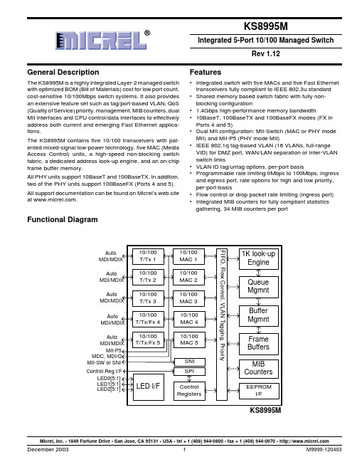
KS8995 – 5 Port 10/100 Switch with PHYIntroductionThe KS8995 contains five 10/100 physical layer transceivers, five MAC (Media Access Control) units with an integrated layer 2 switch. The device runs in two modes. The first mode is a five port integrated switch and the second is as a five port switch with the fifth port decoupled from the physical port. In this mode access to the fifth MAC is provided using a MII (Media Independent Interface).Useful configurations include a stand alone five port switch as well as a four port switch with a routing element connected to the extra MII port. The additional port is also useful for public network interfacing.The KS8995 is designed to reside in an unmanaged design not requiring processor intervention. This is achieved through I/O strapping at system reset timeOn the media side, the KS8995 supports 10BaseT, 100BaseTX and 100BaseFX as specified by the IEEE 802.3 committee.Physical signal transmission and reception are enhanced through use of analog circuitry that makes the design more efficient and allows for lower power consumption and smaller chip die size. Highlights• 5 port 10/100 Integrated Switch with Physical Layer Transceivers•SRAM on chip for frame buffering• 1.4Gbps high performance memory bandwidth •10BaseT, 100BaseTX and 100BaseFX modes of operation•Superior analog technology for reduced power and die size•Single 2.5 V power supply•500 mA (1.25 W) including physical transmit drivers•128 pin PQFP package•Support for UTP or fiber installations •Indicators for link, activity, full / half duplex and speed •Unmanaged operation via strapping at system reset time•Hardware based 10/100, full/half, flow control and auto negotiation•Individual port forced modes (full duplex, 100BaseTX) when auto negotiation is disabled •Wire speed reception and transmission •Integrated address Look-Up Engine, supports 1K absolute MAC addresses•Automatic address learning, address aging and address migration•Broadcast storm protection•Full duplex IEEE 802.3x flow control•Half duplex back pressure flow control •Comprehensive LED support•External MAC interface (MII or SNI) for router applicationsSystem Level ApplicationsThe KS8995 can be configured to fit either in a five port 10/100 application or as a four port 10/100 network interface with an extra MII port. This MII port can be connected to an external processor and used for routing purposes or public network access. The major benefits of using the KS8995 are the lower power consumption, unmanaged operation, flexible configuration and built in frame buffering. Two such applications are depicted below.more informationproducts@。
CS5361-KZZ;CS5361-KSZ;CS5361-DZZ;CS5361-KZZR;CS5361-KSZR;中文规格书,Datasheet资料
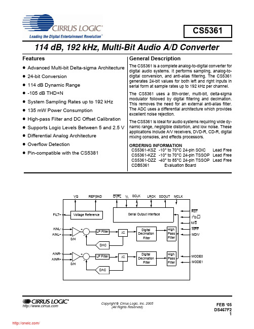
Copyright © Cirrus Logic, Inc. 2005CS5361114 dB, 192 kHz, Multi-Bit Audio A/D ConverterFeaturesz Advanced Multi-bit Delta-sigma Architecture z 24-bit Conversion z 114dB Dynamic Range z -105dB THD+Nz System Sampling Rates up to 192 kHz z 135 mW Power Consumptionz High-pass Filter and DC Offset Calibration z Supports Logic Levels Between 5 and 2.5V z Differential Analog Architecture z Overflow DetectionzPin-compatible with the CS5381General DescriptionThe CS5361 is a complete analog-to-digital converter for digital audio systems. It performs sampling, analog-to-digital conversion, and anti-alias filtering. The CS5361generates 24-bit values for both left and right inputs in serial form at sample rates up to 192kHz per channel.The CS5361 uses a 5th-order, multi-bit, delta-sigma modulator followed by digital filtering and decimation.This removes the need for an external anti-alias filter.The ADC uses a differential architecture which provides excellent noise rejection.The CS5361 is ideal for audio systems requiring wide dy-namic range, negligible distortion, and low noise. These applications include A/V receivers, DVD-R, CD-R, digital mixing consoles, and effects processors.ORDERING INFORMATIONCS5361-KSZ -10° to 70°C 24-pin SOIC Lead Free CS5361-KZZ -10° to 70°C 24-pin TSSOP Lead Free CS5361-DZZ -40° to 85°C 24-pin TSSOP Lead Free CDB5361Evaluation BoardVoltage ReferenceSerial Output InterfaceDigital FilterHighPass FilterHigh Pass FilterDecimation Digital FilterDecimation DAC-+S/HDAC -+S/HAINR+SCLKSDOUT MCLKRST VQ LRCK AINR-AINL+AINL-FILT+I 2S/LJ M/SHPF MODE0MODE1REFGND V L MDIVLP FilterLP Filter∆Σ∆ΣOVFLFEB ‘05TABLE OF CONTENTS1.0 CHARACTERISTICS AND SPECIFICATIONS (4)Specified Operating Conditions (4)Absolute Maximum Ratings (4)Analog Characteristics (CS5361-KSZ/KZZ) (5)Analog Characteristics (CS5361-DZZ) (6)Digital Filter Characteristics (7)DC Electrical Characteristics (10)Digital Characteristics (10)Switching Characteristics - Serial Audio Port (11)2.0 PIN DESCRIPTIONS (14)3.0 TYPICAL CONNECTION DIAGRAM (15)4.0 APPLICATIONS (16)4.1 Operational Mode/Sample Rate Range Select (16)4.2 System Clocking (16)4.2.1 Slave Mode (16)4.2.2 Master Mode (17)4.3 Power-up Sequence (18)4.4 Analog Connections (18)4.5 High-pass Filter and DC Offset Calibration (19)4.6 Overflow Detection (19)4.6.1 OVFL Output Timing (19)4.7 Grounding and Power Supply Decoupling (19)4.8 Synchronization of Multiple Devices (19)5.0 PARAMETER DEFINITIONS (20)6.0 PACKAGE DIMENSIONS (21)7.0 REVISION HISTORY (23)LIST OF FIGURESFigure 1. Single Speed Mode Stopband Rejection (8)Figure 2. Single Speed Mode Transition Band (8)Figure 3. Single Speed Mode Transition Band (Detail) (8)Figure 4. Single Speed Mode Passband Ripple (8)Figure 5. Double Speed Mode Stopband Rejection (8)Figure 6. Double Speed Mode Transition Band (8)Figure 7. Double Speed Mode Transition Band (Detail) (9)Figure 8. Double Speed Mode Passband Ripple (9)Figure 9. Quad Speed Mode Stopband Rejection (9)Figure 10. Quad Speed Mode Transition Band (9)Figure 11. Quad Speed Mode Transition Band (Detail) (9)Figure 12. Quad Speed Mode Passband Ripple (9)Figure 13. Master Mode, Left Justified SAI (12)Figure 14. Slave Mode, Left Justified SAI (12)Figure 15. Master Mode, I2S SAI (12)Figure 16. Slave Mode, I2S SAI (12)Figure 17. OVFL Output Timing (12)Figure 18. Left Justified Serial Audio Interface (13)Figure 19. I2S Serial Audio Interface (13)Figure 20. OVFL Output Timing, I2S Format (13)Figure 21. OVFL Output Timing, Left-Justified Format (13)Figure 22. Typical Connection Diagram (15)Figure 23. CS5361 Master Mode Clocking (17)Figure 24. CS5361 Recommended Analog Input Buffer (18)LIST OF TABLESTable 1.CS5361 Mode Control (16)Table 2.CS5361 Slave Mode Clock Ratios (16)Table 3.CS5361 Common Master Clock Frequencies (17)Table 4.Revision History (23)1.0CHARACTERISTICS AND SPECIFICATIONSAll Min/Max characteristics and specifications are guaranteed over the specified operating conditions. Typical per-formance characteristics and specifications are derived from measurements taken at typical supply voltages and T A = 25°C.SPECIFIED OPERATING CONDITIONSGND = 0V, all voltages with respect to GND.ABSOLUTE MAXIMUM RATINGSGND = 0V, All voltages with respect to GND. (Note 1)Notes: 1.Operation beyond these limits may result in permanent damage to the device.Normal operation is not guaranteed at these extremes.2.Any pin except supplies. Transient currents of up to ±100 mA on the analog input pins will not cause SCRlatch-up.3.The maximum over/under voltage is limited by the input current.ParameterSymbol Min Typ Max Unit DC Power Supplies:Positive Analog Positive Digital Positive LogicVA VD VL 4.753.12.37 5.03.33.3 5.255.255.25V V V Ambient Operating TemperatureCommercial (-KSZ/-KZZ) Automotive (-DZZ)T AC T AA-10-40--7085°C °CParameterSymbol Min Max Units DC Power Supplies:Analog Logic Digital VA VL VD -0.3-0.3-0.3+6.0+6.0+6.0V V V Input Current (Note 2)I in -10+10mA Analog Input Voltage (Note 3)V IN -0.7VA +0.7V Digital Input Voltage(Note 3)V IND -0.7VL +0.7V Ambient Operating Temperature (Power Applied)T A -50+95°C Storage TemperatureT stg-65+150°CANALOG CHARACTERISTICS (CS5361-KSZ/KZZ)Test conditions (unless otherwise specified): Input test signal is a 1kHz sine wave; measurement bandwidth is 10Hz to 20kHz.Notes: 4.Referred to the typical full-scale input voltage.5. Measured between AIN+ and AIN-ParameterSymbolMin Typ Max Unit Single Speed Mode Fs = 48kHzDynamic Range A-weightedunweighted108105114111--dB dBTotal Harmonic Distortion + Noise (Note 4)-1dB -20dB -60dBTHD+N----105-91-51-99--dB dB dB Double Speed Mode Fs = 96kHzDynamic Range A-weightedunweighted40kHz bandwidth unweighted108105-114111108---dB dB dBTotal Harmonic Distortion + Noise (Note 4)-1dB -20dB -60dB40kHz bandwidth -1dBTHD+N-----105-91-51-102-99---dB dB dB dB Quad Speed Mode Fs = 192kHzDynamic Range A-weightedunweighted40kHz bandwidth unweighted108105-114111108---dB dB dBTotal Harmonic Distortion + Noise (Note 4)-1dB -20dB -60dB40kHz bandwidth -1dBTHD+N-----105-91-51-102-99---dB dB dB dB Dynamic Performance for All Modes Interchannel Isolation -110-dB DC AccuracyInterchannel Gain Mismatch -0.1-dB Gain Error -2-2%Gain Drift -100-100ppm/°C Offset Error HPF enabledHPF disabled----0100LSB LSB Analog Input Characteristics Full-scale Input Voltage1.10*VA 1.13*VA1.15*VAVpp Input Impedance (Differential)(Note 5)7.5--k ΩCommon Mode Rejection RatioCMRR-82-dBANALOG CHARACTERISTICS (CS5361-DZZ)Test conditions (unless otherwise specified): Input test signal is a 1kHz sine wave; measurement bandwidth is 10Hz to 20kHz.Parameter Symbol Min Typ Max Unit Single Speed Mode Fs = 48kHzDynamic Range A-weightedunweighted 106103114111--dBdBTotal Harmonic Distortion + Noise(Note 4)-1dB-20dB-60dB THD+N----105-91-51-95--dBdBdBDouble Speed Mode Fs = 96kHzDynamic Range A-weightedunweighted40kHz bandwidth unweighted 106103-114111108---dBdBdBTotal Harmonic Distortion + Noise (Note 4)-1dB-20dB-60dB40kHz bandwidth -1dB THD+N-----105-91-51-102-95---dBdBdBdBQuad Speed Mode Fs = 192kHzDynamic Range A-weightedunweighted40kHz bandwidth unweighted 106103-114111108---dBdBdBTotal Harmonic Distortion + Noise (Note 4)-1dB-20dB-60dB40kHz bandwidth -1dB THD+N-----105-91-51-102-95---dBdBdBdBDynamic Performance for All ModesInterchannel Isolation-110-dB Interchannel Phase Deviation-0.0001-Degree DC AccuracyInterchannel Gain Mismatch-0.1-dB Gain Error-5-5% Gain Drift-100-100ppm/°COffset Error HPF enabledHPF disabled ----100LSBLSBAnalog Input CharacteristicsFull-scale Input Voltage 1.07*VA 1.13*VA 1.18*VA Vpp Input Impedance (Differential)(Note 5)7.5--kΩCommon Mode Rejection Ratio CMRR-82-dBDIGITAL FILTER CHARACTERISTICSNotes: 6.The filter frequency response scales precisely with Fs.7.Response shown is for Fs equal to 48kHz. Filter characteristics scale with Fs.ParameterSymbolMinTypMaxUnitSingle Speed Mode (2kHz to 51kHz sample rates)Passband (-0.1dB)(Note 6)0-0.47Fs Passband Ripple -0.1-0.035dB Stopband(Note 6)0.58--Fs Stopband Attenuation-95--dB Total Group Delay (Fs = Output Sample Rate)t gd-12/Fs -s Interchannel Phase Deviation-0.0001-DegDouble Speed Mode (50kHz to 102kHz sample rates)Passband (-0.1dB)(Note 6)0-0.45Fs Passband Ripple -0.1-0.035dB Stopband(Note 6)0.68--Fs Stopband Attenuation-92--dB Total Group Delay (Fs = Output Sample Rate)t gd-9/Fs -s Interchannel Phase Deviation-0.0001-DegQuad Speed Mode (100kHz to 204kHz sample rates)Passband (-0.1dB)(Note 6)0-0.24Fs Passband Ripple -0.1-0.035dB Stopband(Note 6)0.78--Fs Stopband Attenuation-92--dB Total Group Delay (Fs = Output Sample Rate)t gd-5/Fs -s Interchannel Phase Deviation -0.0001-DegHigh-pass Filter Characteristics Frequency Response -3.0dB -0.13dB (Note 7)-120--Hz Hz Phase Deviation @ 20Hz(Note 7)-10-Deg Passband Ripple --0dB Filter Settling Time105/FssFigure 1. Single Speed Mode Stopband Rejection Figure 2. Single Speed Mode Transition BandFigure 3. Single Speed Mode Transition Band (Detail )Figure 4. Single Speed Mode Passband RippleFigure 7. Double Speed Mode Transition Band (Detail)Figure 8. Double Speed Mode Passband RippleFigure 9. Quad Speed Mode Stopband Rejection Figure 10. Quad Speed Mode Transition BandA m p l i t u d e (dB )F re q u e n c y (n o rm a liz e d to F s )A m p li t u d e (d B )F re q u e n c y (n o rm a liz e d to F s )Figure 11. Quad Speed Mode Transition Band (Detail)Figure 12. Quad Speed Mode Passband RippleF re q u e n c y (n o rm a liz e d to F s )A m p l i t u d e (dB )A m p l i t u d e (dB )F re q u e n c y (n o rm a liz e d to F s )DC ELECTRICAL CHARACTERISTICSGND = 0V, all voltages with respect to ground. MCLK=12.288MHz; Master Mode.Notes:8.Power Down Mode is defined as RST = Low with all clocks and data lines held static.9.Valid with the recommended capacitor values on FILT+ and VQ as shown in the Typical ConnectionDiagram.DIGITAL CHARACTERISTICSTHERMAL CHARACTERISTICSParameterSymbol Min Typ Max Unit Power Supply Current VA = 5V (Normal Operation)VL,VD = 5V VL,VD = 3.3V I A I D I D ---17.52214.521.527.517mA mA mA Power Supply CurrentVA = 5V (Power-Down Mode) (Note 8)VL,VD = 5VI A I D --100100--µA µA Power Consumption (Normal Operation)VA, VD, VL = 5V VA = 5V, VL, VD = 3.3V(Power-Down Mode)------1981351243161-mW mW mW Power Supply Rejection Ratio (1 kHz)(Note 9)PSRR-65-dB V Q Nominal Voltage Output ImpedanceMaximum allowable DC current source/sink --- 2.5250.01---Vk ΩmA Filt+ Nominal Voltage Output ImpedanceMaximum allowable DC current source/sink---5150.01---Vk ΩmAParameterSymbol Min Typ Max Units High-Level Input Voltage (% of VL)V IH 70%--V Low-Level Input Voltage(% of VL)V IL --30%V High-Level Output Voltage at I o = 100µA (% of VL)V OH 70%--V Low-Level Output Voltage at I o = 100µA (% of VL)V OL --15%V OVFL Current SinkI ovfl -- 4.0mA Input Leakage Current (all pins except SCLK and LRCK)I in -10-10µA Input Leakage Current (SCLK and LRCK)I in-25-25µAParameterSymbolMin Typ Max Unit Allowable Junction Temperature--135°C Junction to Ambient Thermal Impedance(Multi-layer PCB) TSSOP (Multi-layer PCB) SOIC (Single-layer PCB) TSSOP (Single-layer PCB) SOICθJA-TM θJA-SM θJA-TS θJA-SS----706010580----°C/W °C/W °C/W °C/W分销商库存信息:CIRRUS-LOGICCS5361-KZZ CS5361-KSZ CS5361-DZZ CS5361-KZZR CS5361-KSZR。
STF9NK90Z中文资料

1/11April 2003STP9NK90Z -STF9NK90ZSTW9NK90ZN-CHANNEL 900V -1.1Ω-8A TO-220/TO-220FP/TO-247Zener-Protected SuperMESH™Power MOSFETs TYPICAL R DS (on)=1.1Ωs EXTREMELY HIGH dv/dt CAPABILITY s 100%AVALANCHE TESTED s GATE CHARGE MINIMIZEDs VERY LOW INTRINSIC CAPACITANCES sVERY GOOD MANUFACTURING REPEATIBILITYDESCRIPTIONThe SuperMESH™series is obtained through an extreme optimization of ST’s well established strip-based PowerMESH™layout.In addition to pushing on-resistance significantly down,special care is tak-en to ensure a very good dv/dt capability for the most demanding applications.Such series comple-ments ST full range of high voltage MOSFET s in-cluding revolutionary MDmesh™products.APPLICATIONSs HIGH CURRENT,HIGH SPEED SWITCHING s SWITCH MODE POWER SUPPLIESs DC-AC CONVERTERS FOR WELDING,UPS AND MOTOR DRIVEORDERING INFORMATIONTYPE V DSS R DS(on)I D Pw STP9NK90Z STF9NK90Z STW9NK90Z900V 900V 900V<1.3Ω<1.3Ω<1.3Ω8A 8A 8A160W 40W 160WSALES TYPE MARKING PACKAGE PACKAGINGSTP9NK90Z P9NK90Z TO-220TUBE STF9NK90Z F9NK90Z TO-220FP TUBE STW9NK90ZW9NK90ZTO-247TUBESTP9NK90Z -STF9NK90Z -STW9NK90Z2/11ABSOLUTE MAXIMUM RATINGS( )Pulse width limited by safe operating area(1)I SD ≤8A,di/dt ≤200A/µs,V DD ≤V (BR)DSS ,T j ≤T JMAX.(*)Limited only by maximum temperature allowedTHERMAL DATAAVALANCHE CHARACTERISTICSGATE-SOURCE ZENER DIODEPROTECTION FEATURES OF GATE-TO-SOURCE ZENER DIODESThe built-in back-to-back Zener diodes have specifically been designed to enhance not only the device’s ESD capability,but also to make them safely absorb possible voltage transients that may occasionally be applied from gate to source.In this respect the Zener voltage is appropriate to achieve an efficient and cost-effective intervention to protect the device’s integrity.These integrated Zener diodes thus avoid the usage of external components.Symbol ParameterValueUnit STP9NK90ZSTF9NK90ZSTW9NK90ZV DS Drain-source Voltage (V GS =0)900V V DGR Drain-gate Voltage (R GS =20k Ω)900V V GS Gate-source Voltage±30VI D Drain Current (continuous)at T C =25°C 88(*)8A I D Drain Current (continuous)at T C =100°C 55(*)5A I DM ( )Drain Current (pulsed)3232(*)32A P TOT Total Dissipation at T C =25°C 16040160W Derating Factor1.280.32 1.28W/°C V ESD(G-S)Gate source ESD(HBM-C=100pF,R=1.5K Ω)4KV dv/dt (1)Peak Diode Recovery voltage slope 4.5V/nsV ISO Insulation Withstand Voltage (DC)-2500-V T j T stgOperating Junction Temperature Storage Temperature-55to 150-55to 150°C °CTO-220TO-220FPTO-247Rthj-case Thermal Resistance Junction-case Max 0.783.10.78°C/W Rthj-ambThermal Resistance Junction-ambient Max62.550°C/W T lMaximum Lead Temperature For Soldering Purpose300°CSymbol ParameterMax ValueUnit I AR Avalanche Current,Repetitive or Not-Repetitive (pulse width limited by T j max)8A E ASSingle Pulse Avalanche Energy(starting T j =25°C,I D =I AR ,V DD =50V)300mJSymbol ParameterTest ConditionsMin.Typ.Max.Unit BV GSOGate-Source Breakdown VoltageIgs=±1mA (Open Drain)30V3/11STP9NK90Z -STF9NK90Z -STW9NK90ZELECTRICAL CHARACTERISTICS (T CASE =25°C UNLESS OTHERWISE SPECIFIED)ON/OFFDYNAMICSWITCHING ONSWITCHING OFFSOURCE DRAIN DIODENote: 1.Pulsed:Pulse duration =300µs,duty cycle 1.5%.2.Pulse width limited by safe operating area.3.C oss eq.is defined as a constant equivalent capacitance giving the same charging time as C oss when V DS increases from 0to 80%V DSS .Symbol ParameterTest ConditionsMin.Typ.Max.Unit V (BR)DSS Drain-sourceBreakdown Voltage I D =1mA,V GS =0900V I DSS Zero Gate VoltageDrain Current (V GS =0)V DS =Max RatingV DS =Max Rating,T C =125°C 150µA µA I GSS Gate-body Leakage Current (V DS =0)V GS =±20V±10µA V GS(th)Gate Threshold Voltage V DS =V GS ,I D =100µA 33.754.5V R DS(on)Static Drain-source On ResistanceV GS =10V,I D =3.6A1.11.3ΩSymbol ParameterTest ConditionsMin.Typ.Max.Unit g fs (1)Forward Transconductance V DS =15V ,I D =3.6A5.75S C iss C oss C rss Input Capacitance Output Capacitance Reverse Transfer Capacitance V DS =25V,f =1MHz,V GS =0211519040pF pF pF C oss eq.(3)Equivalent Output CapacitanceV GS =0V,V DS =0V to 720V115pFSymbol ParameterTest ConditionsMin.Typ.Max.Unit t d(on)t r Turn-on Delay Time Rise TimeV DD =450V,I D =4A R G =4.7ΩV GS =10V(Resistive Load see,Figure 3)2213ns ns Q g Q gs Q gdTotal Gate Charge Gate-Source Charge Gate-Drain ChargeV DD =720V,I D =8A,V GS =10V721438100nC nC nCSymbol ParameterTest ConditionsMin.Typ.Max.Unit t d(off)t f Turn-off Delay Time Fall TimeV DD =450V,I D =4A R G =4.7ΩV GS =10V(Resistive Load see,Figure 3)5528ns ns t r(Voff)t f t cOff-voltage Rise Time Fall TimeCross-over TimeV DD =720V,I D =8A,R G =4.7Ω,V GS =10V(Inductive Load see,Figure 5)531122ns ns nsSymbol ParameterTest ConditionsMin.Typ.Max.Unit I SD I SDM (2)Source-drain CurrentSource-drain Current (pulsed)832A A V SD (1)Forward On Voltage I SD =8A,V GS =0 1.6V t rr Q rr I RRMReverse Recovery Time Reverse Recovery Charge Reverse Recovery CurrentI SD =8A,di/dt =100A/µs V DD =50V,T j =150°C (see test circuit,Figure 5)9501021ns µC ASTP9NK90Z -STF9NK90Z -STW9NK90Z4/11Safe Operating Area For TO-2475/11STP9NK90Z -STF9NK90Z -STW9NK90ZStatic Drain-source On ResistanceTransferCharacteristicsTransconductanceSTP9NK90Z -STF9NK90Z -STW9NK90Z6/11Normalized BVDSS vs TemperatureSource-drain Diode Forward Characteristics7/11STP9NK90Z -STF9NK90Z -STW9NK90ZFig.5:Test Circuit For Inductive Load Switching And Diode Recovery TimesFig.4:Gate Charge test CircuitFig.2:Unclamped Inductive WaveformFig.1:Unclamped Inductive Load TestCircuitFig.3:Switching Times Test Circuit For ResistiveLoadSTP9NK90Z-STF9NK90Z-STW9NK90Z8/11STP9NK90Z-STF9NK90Z-STW9NK90Z9/11STP9NK90Z-STF9NK90Z-STW9NK90Z10/11元器件交易网STP9NK90Z-STF9NK90Z-STW9NK90Z Information furnished is believed to be accurate and reliable. However, STMicroelectronics assumes no responsibility for theconsequences of use of such information nor for any infringement of patents or other rights of third parties which may result fromits use. No license is granted by implication or otherwise under any patent or patent rights of STMicroelectronics. Specificationsmentioned in this publication are subject to change without notice. This publication supersedes and replaces all informationpreviously supplied. STMicroelectronics products are not authorized for use as critical components in life support devices orsystems without express written approval of STMicroelectronics.© The ST logo is a registered trademark of STMicroelectronics© 2003 STMicroelectronics - Printed in Italy - All Rights ReservedSTMicroelectronics GROUP OF COMPANIESAustralia - Brazil - Canada - China - Finland - France - Germany - Hong Kong - India - Israel - Italy - Japan - Malaysia - Malta - MoroccoSingapore - Spain - Sweden - Switzerland - United Kingdom - United States.© 11/11。
KSZ8995M中文资料
General DescriptionThe KS8995M is a highly integrated Layer-2 managed switchwith optimized BOM (Bill of Materials) cost for low port count,cost-sensitive 10/100Mbps switch systems. It also provides an extensive feature set such as tag/port-based VLAN, QoS (Quality of Service) priority, management, MIB counters, dual MII interfaces and CPU control/data interfaces to effectively address both current and emerging Fast Ethernet applica-tions.The KS8995M contains five 10/100 transceivers with pat-ented mixed-signal low-power technology, five MAC (Media Access Control) units, a high-speed non-blocking switch fabric, a dedicated address look-up engine, and an on-chip frame buffer memory.All PHY units support 10BaseT and 100BaseTX. In addition,two of the PHY units support 100BaseFX (Ports 4 and 5).All support documentation can be found on Micrel’s web site at .Features•Integrated switch with five MACs and five Fast Ethernet transceivers fully compliant to IEEE 802.3u standard •Shared memory based switch fabric with fully non-blocking configuration• 1.4Gbps high-performance memory bandwidth•10BaseT, 100BaseTX and 100BaseFX modes (FX in Ports 4 and 5)•Dual MII configuration: MII-Switch (MAC or PHY mode MII) and MII-P5 (PHY mode MII)•IEEE 802.1q tag-based VLAN (16 VLANs, full-range VID) for DMZ port, WAN/LAN separation or inter-VLAN switch links•VLAN ID tag/untag options, per-port basis•Programmable rate limiting 0Mbps to 100Mbps, ingress and egress port, rate options for high and low priority,per-port-basis•Flow control or drop packet rate limiting (ingress port)•Integrated MIB counters for fully compliant statistics gathering, 34 MIB counters per portMicrel, Inc. • 1849 Fortune Drive • San Jose, CA 95131 • USA • tel + 1 (408) 944-0800 • fax + 1 (408) 944-0970 • Functional DiagramAuto Auto Auto Auto Auto KS8995MFeatures (continued)•Enable/Disable option for huge frame size up to 1916 bytes per frame•IGMP v1/v2 snooping for multicast packet filtering •Special tagging mode to send CPU info on ingress packet’s port value•SPI slave (complete) and MDIO (MII PHY only) serial management interface for control of register configura-tion•MAC-id based security lock option•Control registers configurable on-the-fly (port-priority, 802.1p/d/q, AN...)•CPU read access to MAC forwarding table entries •802.1d Spanning Tree Protocol•Port mirroring/monitoring/sniffing:ingress and/or egress traffic to any port or MII•Broadcast storm protection with percent control–global and per-port basis•Optimization for fiber-to-copper media conversion •Full-chip hardware power-down support (register configuration not saved)•Per-port based software power-save on PHY (idle link detection, register configuration preserved)•QoS/CoS packets prioritization supports: per port, 802.1p and DiffServ based•802.1p/q tag insertion or removal on a per port basis (egress)•MDC and MDI/O interface support to access the MII PHY control registers (not all control registers)•MII local loopback support•On-chip 64Kbyte memory for frame buffering (not shared with 1K unicast address table)•Wire-speed reception and transmission•Integrated look-up engine with dedicated 1K MAC addresses•Full duplex IEEE 802.3x and half-duplex back pressure flow control•Comprehensive LED support•7-wire SNI support for legacy MAC interface •Automatic MDI/MDI-X crossover for plug-and-play •Disable Automatic MDI/MDI-X option•Low power:Core:1.8VI/O:2.5V or 3.3V•0.18µm CMOS technology•Commercial temperature range:0°C to +70°C •Industrial temperature range:–40°C to +85°C •Available in 128-pin PQFP package Applications•Broadband gateway/firewall/VPN•Integrated DSL or cable modem multi-port router •Wireless LAN access point plus gateway•Home networking expansion•Standalone 10/100 switch•Hotel/campus/MxU gateway•Enterprise VoIP gateway/phone•FTTx customer premise equipment•Managed media converterOrdering InformationPart Number Temperature Range PackageKS8995M0°C to +70°C128-Pin PQFPKSZ8995M0°C to +70°C128-Pin PQFP Lead Free KS8995MI–40°C to +85°C128-Pin PQFPRevision HistoryRevision Date Summary of Changes1.0011/05/01Created1.0111/09/01Pinout Mux1/2, DVCC-IO2.5/3.3V, feature list, register spec 11-091.0212/03/01Editorial changes, added new register and MIB descriptions. Added paragraph describing TOS registers.Imported functional descriptions. Formatting.1.0312/12/01Incorporate changes per engineering feedback as well as updating functional descriptions and addingnew timing information.1.0412/13/01Changed Rev. and For. Modes to PHY and MAC modes respectively. Added MIIM clarification in “MIIManagement Interface” section. Reformatted section sequence. Added hex register addresses. Addedadvertisement ability descriptions.1.0512/18/01Inserted switch forwarding flow charts.1.0612/20/01Added new KS8995M block diagram, editorial changes, register descriptions changes and cross-references from functional descriptions to register and strap in options.1.071/22/01Changed FXSD pins to inputs, added new descriptions to “Configuration Interfaces” section.Edited pin descriptions.1.083/1/02Editorial changes in “Dynamic MAC Address table and “MIB Counters.” Updated figure 2 flowchart.Updated table 2 for MAC mode connections. Separate static MAC bit assignments for read and write.Edited read and write examples to MAC tables and MIB counters. Changed Table 3 KS8995M signals to“S” suffix. Changed aging description in Register 2, bit 0. Changed “Port Registers” section and listed allport register addresses. Changed port control 11 description for bits [7:5]. Changed MIB counterdescriptions.1.095/17/02Changed MII setting in “Pin Descriptions.” Changed pu/pd descriptions for SMRXD2. “Register 18,”changed pu/pd description for forced flow control. “Illegal Frames. ” Edited large packet sizes back in.“Elecrical Characteristics,” Added in typical supply current numbers for 100 BaseTX and 10 BaseTXoperation. “Register 18,” Added in note for illegal half-duplex, force flow control. “Pin Description,” Addedextra X1 clock input description. “Elecrical Characteristics,” Updated to chip only current numbers.Added SPI Timing. Feature Highlights.1.107/29/02“Pin Description,” changed SMRXC and SMTXC to I/O. Input in MAC mode, output in PHY mode MII.“Elecrical Characteristics,” modified current consumption to chip only numbers. “Half-Duplex BackPressure,” added description for no dropped packets in half-duplex mode. Added recommendedoperating conditions. Added Idle mode current consumption in “Elecrical Characteristics,” added“Selection of Isolation Transformers,” Added 3.01kΩ resistor instructions for ISET “Pin Description”section. Changed Polarity of transmit pairs in “Pin Description.” Changed description for Register 2, bit 1,in “Register Description” section. Added “Reset Timing” section.1.1112/17/02“Register 3” changed 802.1x to 802.3x. “Register 6,” changed default column to disable flow control forpull-down, and enable flow control for pull-up. “Register 29” and “Register 0” indicate loop back is at thePHY. Added description to register 4 bit 2 to indicate that STPID packets from CPU to normal ports arenot allowed as 1522 byte tag packets. Fixed dynamic MAC address example errors in “Dynamic MACAddress Table.” Changed definition of forced MDI, MDIX in section “Register 29,”“Register 30” and“Register 0.” Added “Part Ordering Information.” Added Ambient operating temperature for KS8995MI 1.123/10/03Changed pin 120 description to NC. Changed SPIQ pin description to Otri. Changed logo. Changedcontact information.Table of ContentsSystem Level Applications (7)Pin Description (by Number) (9)Pin Description (by Name) (15)Pin Configuration (21)Introduction (22)Functional Overview:Physical Layer Transceiver (22)100BaseTX Transmit (22)100BaseTX Receive (22)PLL Clock Synthesizer (22)Scrambler/De-scrambler (100BaseTX only) (22)100BaseFX Operation (22)100BaseFX Signal Detection (22)100BaseFX Far End Fault (23)10BaseT Transmit (23)10BaseT Receive (23)Power Management (23)MDI/MDI-X Auto Crossover (23)Auto-Negotiation (23)Functional Overview:Switch Core (24)Address Look-Up (24)Learning (24)Migration (24)Aging (24)Forwarding (24)Switching Engine (24)MAC Operation (24)Inter-Packet Gap (IPG) (24)Backoff Algorithm (24)Late Collision (26)Illegal Frames (26)Flow Control (26)Half-Duplex Back Pressure (26)Broadcast Storm Protection (26)MII Interface Operation (26)SNI Interface Operation (28)Advanced Functionality (28)Spanning Tree Support (28)Special Tagging Mode (29)IGMP Support (30)Port Mirroring Support (31)VLAN Support (31)Rate Limit Support (32)Configuration Interface (33)I2C Master Serial Bus Configuration (35)SPI Slave Serial Bus Configuration (35)MII Management Interface (MIIM) (38)Register Description (39)Global Registers (39)Register 0 (0x00): Chip ID0 (39)Register 1 (0x01): Chip ID1/Start Switch (39)Register 2 (0x02): Global Control 0 (40)Register 3 (0x03): Global Control 1 (40)Register 4 (0x04): Global Control 2 (41)Register 5 (0x05): Global Control 3 (42)Register 6 (0x06): Global Control 4 (42)Register 7 (0x07): Global Control 5 (43)Register 8 (0x08): Global Control 6 (43)Register 9 (0x09): Global Control 7 (43)Register 10 (0x0A): Global Control 8 (43)Register 11 (0x0B): Global Control 9 (43)Port Registers (44)Register 16 (0x10):Port 1 Control 0 (44)Register 17 (0x11):Port 1 Control 1 (44)Register 18 (0x12):Port 1 Control 2 (45)Register 19 (0x13):Port 1 Control 3 (46)Register 20 (0x14):Port 1 Control 4 (46)Register 21 (0x15):Port 1 Control 5 (46)Register 22 (0x16):Port 1 Control 6 (46)Register 23 (0x17):Port 1 Control 7 (46)Register 24 (0x18):Port 1 Control 8 (47)Register 25 (0x19):Port 1 Control 9 (47)Register 26 (0x1A):Port 1 Control 10 (47)Register 27 (0x1B):Port 1 Control 11 (47)Register 28 (0x1C):Port 1 Control 12 (48)Register 29 (0x1D):Port 1 Control 13 (49)Register 30 (0x1E):Port 1 Status 0 (49)Register 31 (0x1F):Port 1 Status 1 (50)Advanced Control Registers (50)Register 96 (0x60):TOS Priority Control Register 0 (50)Register 97 (0x61):TOS Priority Control Register 1 (50)Register 98 (0x62):TOS Priority Control Register 2 (50)Register 99 (0x63):TOS Priority Control Register 3 (50)Register 100 (0x64):TOS Priority Control Register 4 (50)Register 101 (0x65):TOS Priority Control Register 5 (50)Register 102 (0x66):TOS Priority Control Register 6 (50)Register 103 (0x67):TOS Priority Control Register 7 (50)Register 104 (0x68):MAC Address Register 0 (50)Register 105 (0x69):MAC Address Register 1 (50)Register 106 (0x6A):MAC Address Register 2 (50)Register 107 (0x6B):MAC Address Register 3 (50)Register 108 (0x6C):MAC Address Register 4 (50)Register 109 (0X6D):MAC Address Register 5 (50)Register 110 (0x6E):Indirect Access Control 0 (51)Register 111 (0x6F):Indirect Access Control 1 (51)Register 112 (0x70):Indirect Data Register 8 (51)Register 113 (0x71):Indirect Data Register 7 (51)Register 114 (0x72):Indirect Data Register 6 (51)Register 115 (0x73):Indirect Data Register 5 (51)Register 116 (0x74):Indirect Data Register 4 (51)Register 117 (0x75):Indirect Data Register 3 (51)Register 118 (0x76):Indirect Data Register 2 (51)Register 119 (0x77):Indirect Data Register 1 (51)Register 120 (0x78):Indirect Data Register 0 (51)Register 121 (0x79):Digital Testing Status 0 (51)Register 122 (0x7A):Digital Testing Status 1 (51)Register 123 (0x7B):Digital Testing Control 0 (51)Register 124 (0x7C):Digital Testing Control 1 (51)Register 125 (0x7D):Analog Testing Control 0 (51)Register 126 (0x7E):Analog Testing Control 1 (52)Register 127 (0x7F):Analog Testing Status (52)Static MAC Address (53)VLAN Address (55)Dynamic MAC Address (56)MIB Counters (57)MIIM Registers (60)Register 0: MII Control (60)Register 1: MII Status (61)Register 2: PHYID HIGH (61)Register 3: PHYID LOW (61)Register 4: Advertisement Ability (61)Register 5: Link Partner Ability (62)Absolute Maximum Ratings (63)Operating Ratings (63)Electrical Characteristics (63)Timing Diagrams (65)Selection of Isolation Transformers (72)Qualified Magnetic Lists (72)Package Information (73)System Level Applications4-port LAN1-portWAN I/FFigure 1.Broadband Gateway4-port LANFigure 2.Integrated Broadband Router5-port LANFigure 3.Standalone SwitchPin Description (by Number)Pin Number Pin Name Type(1)Port Pin Function1TEST1NC NC for normal operation. Factory test pin.2GNDA Gnd Analog ground3VDDAR P 1.8V analog V DD4RXP1I1Physical receive signal + (differential)5RXM1I1Physical receive signal - (differential)6GNDA Gnd Analog ground7TXM1O1Physical transmit signal - (differential)8TXP1O1Physical transmit signal + (differential)9VDDAT P 2.5V analog V DD10RXP2I2Physical receive signal + (differential)11RXM2I2Physical receive signal - (differential)12GNDA Gnd Analog ground13TXM2O2Physical transmit signal - (differential)14TXP2O2Physical transmit signal + (differential)15VDDAR P 1.8V analog V DD16GNDA Gnd Analog ground17ISET Set physical transmit output current. Pull-down with a 3.01kΩ 1%resistor.18VDDAT P 2.5V analog V DD19RXP3I3Physical receive signal + (differential)20RXM3I3Physical receive signal - (differential)21GNDA Gnd Analog ground22TXM3O3Physical transmit signal - (differential)23TXP3O3Physical transmit signal + (differential)24VDDAT P 2.5V analog V DD25RXP4I4Physical receive signal + (differential)26RXM4I4Physical receive signal - (differential)27GNDA Gnd Analog ground28TXM4O4Physical transmit signal - (differential)29TXP4O4Physical transmit signal + (differential)30GNDA Gnd Analog ground31VDDAR P 1.8V analog V DDNote:1.P = Power supplyI = InputO = OutputI/O = Bi-directionalGnd = GroundIpu = Input w/ internal pull-upIpd = Input w/ internal pull-downIpd/O = Input w/ internal pull-down during reset, output pin otherwiseIpu/O = Input w/ internal pull-up during reset, output pin otherwisePU = Strap pin pull-upPD = Strap pin pull-downOtri = Output tristatedNC = No ConnectPin Number Pin Name Type(1)Port Pin Function32RXP5I5Physical receive signal + (differential)33RXM5I5Physical receive signal - (differential)34GNDA Gnd Analog ground35TXM5O5Physical transmit signal - (differential)36TXP5O5Physical transmit signal + (differential)37VDDAT P 2.5V analog V DD38FXSD5I5Fiber signal detect/factory test pin39FXSD4I4Fiber signal detect/factory test pin40GNDA Gnd Analog ground41VDDAR P 1.8V analog V DD42GNDA Gnd Analog ground43VDDAR P 1.8V analog V DD44GNDA Gnd Analog ground45MUX1NC MUX1 and MUX2 should be left unconnected for normal operation.46MUX2NC They are factory test pins.Mode Mux1Mux2Normal Operation NC NCRemote Analog Loopback Mode for Testing only01Reserved10Power Save Mode for Testing only11 47PWRDN_N Ipu Full-chip power down. Active low.48RESERVE NC Reserved pin. No connect.49GNDD Gnd Digital ground50VDDC P 1.8V digital core V DD51PMTXEN Ipd5PHY[5] MII transmit enable52PMTXD3Ipd5PHY[5] MII transmit bit 353PMTXD2Ipd5PHY[5] MII transmit bit 254PMTXD1Ipd5PHY[5] MII transmit bit 155PMTXD0Ipd5PHY[5] MII transmit bit 056PMTXER Ipd5PHY[5] MII transmit error57PMTXC O5PHY[5] MII transmit clock. PHY mode MII.58GNDD Gnd Digital groundNote:1.P = Power supplyI = InputO = OutputI/O = Bi-directionalGnd = GroundIpu = Input w/ internal pull-upIpd = Input w/ internal pull-downIpd/O = Input w/ internal pull-down during reset, output pin otherwiseIpu/O = Input w/ internal pull-up during reset, output pin otherwisePU = Strap pin pull-upPD = Strap pin pull-downOtri = Output tristatedNC = No ConnectPin Number Pin Name Type(1)Port Pin Function59VDDIO P 3.3/2.5V digital V DD for digital I/O circuitry60PMRXC O5PHY[5] MII receive clock. PHY mode MII61PMRXDV Ipd/O5PHY[5] MII receive data valid62PMRXD3Ipd/O5PHY[5] MII receive bit 3. Strap option:PD (default) = enable flowcontrol; PU = disable flow control.63PMRXD2Ipd/O5PHY[5] MII receive bit 2. Strap option:PD (default) = disable backpressure; PU = enable back pressure.64PMRXD1Ipd/O5PHY[5] MII receive bit 1. Strap option:PD (default) = drop excessivecollision packets; PU = does not drop excessive collision packets.65PMRXD0Ipd/O5PHY[5] MII receive bit 0. Strap option: PD (default) = disableaggressive back-off algorithm in half-duplex mode; PU = enable forperformance enhancement.66PMRXER Ipd/O5PHY[5] MII receive error. Strap option:PD (default) = 1522/1518 bytes;PU = packet size up to 1536 bytes.67PCRS Ipd/O5PHY[5] MII carrier sense/Force duplex mode. See “Register 76” forport 4 only. PD (default) = Force half-duplex if auto-negotiation isdisabled or fails. PU = Force full-duplex if auto-negotiation is disabledor fails.68PCOL Ipd/O5PHY[5] MII collision detect/ Force flow control. See “Register 66” forport 4 only. PD (default) = No force flow control. PU = Force flowcontrol.69SMTXEN Ipd Switch MII transmit enable70SMTXD3Ipd Switch MII transmit bit 371SMTXD2Ipd Switch MII transmit bit 272SMTXD1Ipd Switch MII transmit bit 173SMTXD0Ipd Switch MII transmit bit 074SMTXER Ipd Switch MII transmit error75SMTXC I/O Switch MII transmit clock. Input in MAC mode, output in PHY mode MII.76GNDD Gnd Digital ground77VDDIO P 3.3/2.5V digital V DD for digital I/O circuitry78SMRXC I/O Switch MII receive clock. Input in MAC mode, output in PHY mode MII.79SMRXDV Ipd/O Switch MII receive data valid80SMRXD3Ipd/O Switch MII receive bit 3. Strap option: PD (default) = Disable Switch MIIfull-duplex flow control; PU = Enable Switch MII full-duplex flow control.81SMRXD2Ipd/O Switch MII receive bit 2. Strap option: PD (default) = Switch MII in full-duplex mode; PU = Switch MII in half-duplex mode.Note:1.P = Power supplyI = InputO = OutputI/O = Bi-directionalGnd = GroundIpu = Input w/ internal pull-upIpd = Input w/ internal pull-downIpd/O = Input w/ internal pull-down during reset, output pin otherwiseIpu/O = Input w/ internal pull-up during reset, output pin otherwisePU = Strap pin pull-upPD = Strap pin pull-downOtri = Output tristatedNC = No ConnectPin Number Pin Name Type(1)Port Pin Function82SMRXD1Ipd/O Switch MII receive bit 1. Strap option: PD (default) = Switch MII in100Mbps mode; PU = Switch MII in 10Mbps mode.83SMRXD0Ipd/O Switch MII receive bit 0; Strap option: LED ModePD (default) = Mode 0; PU = Mode 1. See “Register 11.”Mode 0Mode 1LEDX_2Lnk/Act100Lnk/ActLEDX_1Fulld/Col10Lnk/ActLEDX_0Speed Fulld 84SCOL Ipd/O Switch MII collision detect85SCRS Ipd/O Switch MII carrier sense86SCONF1Ipd Dual MII configuration pinPin# (91, 86, 87):Switch MII PHY [5] MII000Disable, Otri Disable, Otri001PHY Mode MII Disable, Otri010MAC Mode MII Disable, Otri011PHY Mode SNI Disable, Otri100Disable Disable101PHY Mode MII PHY Mode MII110MAC Mode MII PHY Mode MII111PHY Mode SNI PHY Mode MII 87SCONF0Ipd Dual MII configuration pin88GNDD Gnd Digital ground89VDDC P 1.8V digital core V DD90LED5-2Ipu/O5LED indicator 2. Strap option: Aging setup. See “Aging” sectionPU (default) = Aging Enable; PD = Aging disable.91LED5-1Ipu/O5LED indicator 1. Strap option: PU (default): enable PHY MII I/FPD:tristate all PHY MII output. See “pin# 86 SCONF1.”92LED5-0Ipu/O5LED indicator 093LED4-2Ipu/O4LED indicator 294LED4-1Ipu/O4LED indicator 195LED4-0Ipu/O4LED indicator 096LED3-2Ipu/O3LED indicator 297LED3-1Ipu/O3LED indicator 1Note:1.P = Power supplyI = InputO = OutputI/O = Bi-directionalGnd = GroundIpu = Input w/ internal pull-upIpd = Input w/ internal pull-downIpd/O = Input w/ internal pull-down during reset, output pin otherwiseIpu/O = Input w/ internal pull-up during reset, output pin otherwisePU = Strap pin pull-upPD = Strap pin pull-downOtri = Output tristatedNC = No ConnectPin Number Pin Name Type(1)Port Pin Function98LED3-0Ipu/O3LED indicator 099GNDD Gnd Digital ground100VDDIO P 3.3/2.5V digital V DD for digital I/O101LED2-2Ipu/O2LED indicator 2102LED2-1Ipu/O2LED indicator 1103LED2-0Ipu/O2LED indicator 0104LED1-2Ipu/O1LED indicator 2105LED1-1Ipu/O1LED indicator 1106LED1-0Ipu/O1LED indicator 0107MDC Ipu All Switch or PHY[5] MII management data clock108MDIO I/O All Switch or PHY[5] MII management data I/O.Features internal pull down to define pin state when not driven.109SPIQ Otri All(1) SPI serial data output in SPI slave mode; (2) Not used in I2C mastermode. See “pin# 113.”110SPIC/SCL I/O All(1) Input clock up to 5MHz in SPI slave mode; (2) Output clock at81KHz in I2C master mode. See “pin# 113.”111SPID/SDA I/O All(1) Serial data input in SPI slave mode; (2) Serial data input/output inI2C master mode See “pin# 113.”112SPIS_N Ipu All Active low. (1) SPI data transfer start in SPI slave mode. When SPIS_Nis high, the KS8995M is deselected and SPIQ is held in high impedancestate, a high-to-low transition to initiate the SPI data transfer; (2) Notused in I2C master mode.113PS1Ipd Serial bus configuration pinIf EEPROM is not present, the KS8995M will start itself with chipdefault (00)...Pin Config.Serial Bus ConfigurationPS[1:0]=00I2C Master Mode for EEPROMPS[1:0]=01ReservedPS[1:0]=10SPI Slave Mode for CPU InterfacePS[1:0]=11Factory Test Mode (BIST) 114PS0Ipd Serial bus configuration pin. See “pin# 113.”115RST_N Ipu Reset the KS8995M. Active low.116GNDD Gnd Digital ground117VDDC P 1.8V digital core V DD118TESTEN Ipd NC for normal operation. Factory test pin.Note:1.P = Power supplyI = InputO = OutputI/O = Bi-directionalGnd = GroundIpu = Input w/ internal pull-upIpd = Input w/ internal pull-downIpd/O = Input w/ internal pull-down during reset, output pin otherwiseIpu/O = Input w/ internal pull-up during reset, output pin otherwisePU = Strap pin pull-upPD = Strap pin pull-downOtri = Output tristatedNC = No ConnectPin Number Pin Name Type(1)Port Pin Function119SCANEN Ipd NC for normal operation. Factory test pin.120NC NC No Connect121X1I25MHz crystal clock connection/or 3.3V tolerant oscillator input.Oscillator should be ±100ppm.122X2O25MHz crystal clock connection123VDDAP P 1.8V analog V DD for PLL124GNDA Gnd Analog ground125VDDAR P 1.8V analog V DD126GNDA Gnd Analog ground127GNDA Gnd Analog ground128TEST2NC NC for normal operation. Factory test pin.Note:1.P = Power supplyI = InputO = OutputI/O = Bi-directionalGnd = GroundIpu = Input w/ internal pull-upIpd = Input w/ internal pull-downIpd/O = Input w/ internal pull-down during reset, output pin otherwiseIpu/O = Input w/ internal pull-up during reset, output pin otherwisePU = Strap pin pull-upPD = Strap pin pull-downOtri = Output tristatedNC = No ConnectPin Description (by Name)Pin Number Pin Name Type(1)Port Pin Function39FXSD4I4Fiber signal detect/factory test pin.38FXSD5I5Fiber signal detect/factory test pin.124GNDA Gnd Analog ground42GNDA Gnd Analog ground44GNDA Gnd Analog ground2GNDA Gnd Analog ground16GNDA Gnd Analog ground30GNDA Gnd Analog ground6GNDA Gnd Analog ground12GNDA Gnd Analog ground21GNDA Gnd Analog ground27GNDA Gnd Analog ground34GNDA Gnd Analog ground40GNDA Gnd Analog ground120NC NC No connect127GNDA Gnd Analog ground126GNDA Gnd Analog ground49GNDD Gnd Digital ground88GNDD Gnd Digital ground116GNDD Gnd Digital ground58GNDD Gnd Digital ground76GNDD Gnd Digital ground99GNDD Gnd Digital ground17ISET Set physical transmit output current. Pull-down with a 3.01kΩ 1%resistor.106LED1-0Ipu/O1LED indicator 0105LED1-1Ipu/O1LED indicator 1104LED1-2Ipu/O1LED indicator 2103LED2-0Ipu/O2LED indicator 0102LED2-1Ipu/O2LED indicator 1101LED2-2Ipu/O2LED indicator 298LED3-0Ipu/O3LED indicator 0Note:1.P = Power supplyI = InputO = OutputI/O = Bi-directionalGnd = GroundIpu = Input w/ internal pull-upIpd = Input w/ internal pull-downIpd/O = Input w/ internal pull-down during reset, output pin otherwiseIpu/O = Input w/ internal pull-up during reset, output pin otherwisePU = Strap pin pull-upPD = Strap pin pull-downOtri = Output tristatedNC = No ConnectPin Number Pin Name Type(1)Port Pin Function97LED3-1Ipu/O3LED indicator 196LED3-2Ipu/O3LED indicator 295LED4-0Ipu/O4LED indicator 094LED4-1Ipu/O4LED indicator 193LED4-2Ipu/O4LED indicator 292LED5-0Ipu/O5LED indicator 091LED5-1Ipu/O5LED indicator 1. Strap option:PU (default): enable PHY MII I/F.PD:tristate all PHY MII output. See “pin# 86 SCONF1.”90LED5-2Ipu/O5LED indicator 2. Strap option: Aging setup. See “Aging” section.(default) = Aging Enable;PD = Aging disable 107MDC Ipu All Switch or PHY[5] MII management data clock.108MDIO I/O All Switch or PHY[5] MII management data I/O.1TEST1NC NC for normal operation. Factory test pin.45MUX1NC MUX1 and MUX2 should be left unconnected for normal operation.46MUX2NC They are factory test pins.Mode Mux1Mux2Normal Operation NC NCRemote Analog Loopback Mode for Testing only01Reserved10Power Save Mode for Testing only11 68PCOL Ipd/O5PHY[5] MII collision detect/Force flow control. See “Register 18.”For port 4 only. PD (default) = No force flow control. PU = Force flowcontrol.67PCRS Ipd/O5PHY[5] MII carrier sense/Force duplex mode See “Register 28.”For port 4 only. PD (default) = Force half-duplex if auto-negotiation isdisabled or fails. PU = Force full-duplex if auto-negotiation is disabledor fails.60PMRXC O5PHY[5] MII receive clock. PHY mode MII.65PMRXD0Ipd/O5PHY[5] MII receive bit 0. Strap option: PD (default) = disableaggressive back-off algorithm in half-duplex mode; PU = enable forperformance enhancement.64PMRXD1Ipd/O5PHY[5] MII receive bit 1. Strap option: PD (default) = drop excessivecollision packets; PU = does not drop excessive collision packets.63PMRXD2Ipd/O5PHY[5] MII receive bit 2. Strap option: PD (default) = disable backpressure; PU = enable back pressure.62PMRXD3Ipd/O5PHY[5] MII receive bit 3. Strap option: PD (default) = enable flowcontrol; PU = disable flow control.Note:1.P = Power supplyI = InputO = OutputI/O = Bi-directionalGnd = GroundIpu = Input w/ internal pull-upIpd = Input w/ internal pull-downIpd/O = Input w/ internal pull-down during reset, output pin otherwiseIpu/O = Input w/ internal pull-up during reset, output pin otherwisePU = Strap pin pull-upPD = Strap pin pull-downOtri = Output tristatedNC = No Connect。
KSZ8995M,KSZ8995M,KS8995M,KS8995MI, 规格书,Datasheet 资料

General DescriptionThe KS8995M is a highly integrated Layer-2 managed switch with optimized BOM (Bill of Materials) cost for low port count,cost-sensitive 10/100Mbps switch systems. It also provides an extensive feature set such as tag/port-based VLAN, QoS (Quality of Service) priority, management, MIB counters, dual MII interfaces and CPU control/data interfaces to effectively address both current and emerging Fast Ethernet applica-tions.The KS8995M contains five 10/100 transceivers with pat-ented mixed-signal low-power technology, five MAC (Media Access Control) units, a high-speed non-blocking switch fabric, a dedicated address look-up engine, and an on-chip frame buffer memory.All PHY units support 10BaseT and 100BaseTX. In addition,two of the PHY units support 100BaseFX (Ports 4 and 5).All support documentation can be found on Micrel’s web site at .Features•Integrated switch with five MACs and five Fast Ethernet transceivers fully compliant to IEEE 802.3u standard •Shared memory based switch fabric with fully non-blocking configuration• 1.4Gbps high-performance memory bandwidth•10BaseT, 100BaseTX and 100BaseFX modes (FX in Ports 4 and 5)•Dual MII configuration: MII-Switch (MAC or PHY mode MII) and MII-P5 (PHY mode MII)•IEEE 802.1q tag-based VLAN (16 VLANs, full-range VID) for DMZ port, WAN/LAN separation or inter-VLAN switch links•VLAN ID tag/untag options, per-port basis•Programmable rate limiting 0Mbps to 100Mbps, ingress and egress port, rate options for high and low priority,per-port-basis•Flow control or drop packet rate limiting (ingress port)•Integrated MIB counters for fully compliant statistics gathering, 34 MIB counters per portMicrel, Inc. • 1849 Fortune Drive • San Jose, CA 95131 • USA • tel + 1 (408) 944-0800 • fax + 1 (408) 944-0970 • Functional DiagramAuto Auto Auto Auto Auto KS8995MFeatures (continued)•Enable/Disable option for huge frame size up to 1916 bytes per frame•IGMP v1/v2 snooping for multicast packet filtering •Special tagging mode to send CPU info on ingress packet’s port value•SPI slave (complete) and MDIO (MII PHY only) serial management interface for control of register configura-tion•MAC-id based security lock option•Control registers configurable on-the-fly (port-priority, 802.1p/d/q, AN...)•CPU read access to MAC forwarding table entries •802.1d Spanning Tree Protocol•Port mirroring/monitoring/sniffing:ingress and/or egress traffic to any port or MII•Broadcast storm protection with percent control–global and per-port basis•Optimization for fiber-to-copper media conversion •Full-chip hardware power-down support (register configuration not saved)•Per-port based software power-save on PHY (idle link detection, register configuration preserved)•QoS/CoS packets prioritization supports: per port, 802.1p and DiffServ based•802.1p/q tag insertion or removal on a per port basis (egress)•MDC and MDI/O interface support to access the MII PHY control registers (not all control registers)•MII local loopback support•On-chip 64Kbyte memory for frame buffering (not shared with 1K unicast address table)•Wire-speed reception and transmission•Integrated look-up engine with dedicated 1K MAC addresses•Full duplex IEEE 802.3x and half-duplex back pressure flow control•Comprehensive LED support•7-wire SNI support for legacy MAC interface •Automatic MDI/MDI-X crossover for plug-and-play •Disable Automatic MDI/MDI-X option•Low power:Core:1.8VI/O:2.5V or 3.3V•0.18µm CMOS technology•Commercial temperature range:0°C to +70°C •Industrial temperature range:–40°C to +85°C •Available in 128-pin PQFP package Applications•Broadband gateway/firewall/VPN•Integrated DSL or cable modem multi-port router •Wireless LAN access point plus gateway•Home networking expansion•Standalone 10/100 switch•Hotel/campus/MxU gateway•Enterprise VoIP gateway/phone•FTTx customer premise equipment•Managed media converterOrdering InformationPart Number Temperature Range PackageKS8995M0°C to +70°C128-Pin PQFPKSZ8995M0°C to +70°C128-Pin PQFP Lead Free KS8995MI–40°C to +85°C128-Pin PQFPRevision HistoryRevision Date Summary of Changes1.0011/05/01Created1.0111/09/01Pinout Mux1/2, DVCC-IO2.5/3.3V, feature list, register spec 11-091.0212/03/01Editorial changes, added new register and MIB descriptions. Added paragraph describing TOS registers.Imported functional descriptions. Formatting.1.0312/12/01Incorporate changes per engineering feedback as well as updating functional descriptions and addingnew timing information.1.0412/13/01Changed Rev. and For. Modes to PHY and MAC modes respectively. Added MIIM clarification in “MIIManagement Interface” section. Reformatted section sequence. Added hex register addresses. Addedadvertisement ability descriptions.1.0512/18/01Inserted switch forwarding flow charts.1.0612/20/01Added new KS8995M block diagram, editorial changes, register descriptions changes and cross-references from functional descriptions to register and strap in options.1.071/22/01Changed FXSD pins to inputs, added new descriptions to “Configuration Interfaces” section.Edited pin descriptions.1.083/1/02Editorial changes in “Dynamic MAC Address table and “MIB Counters.” Updated figure 2 flowchart.Updated table 2 for MAC mode connections. Separate static MAC bit assignments for read and write.Edited read and write examples to MAC tables and MIB counters. Changed Table 3 KS8995M signals to“S” suffix. Changed aging description in Register 2, bit 0. Changed “Port Registers” section and listed allport register addresses. Changed port control 11 description for bits [7:5]. Changed MIB counterdescriptions.1.095/17/02Changed MII setting in “Pin Descriptions.” Changed pu/pd descriptions for SMRXD2. “Register 18,”changed pu/pd description for forced flow control. “Illegal Frames. ” Edited large packet sizes back in.“Elecrical Characteristics,” Added in typical supply current numbers for 100 BaseTX and 10 BaseTXoperation. “Register 18,” Added in note for illegal half-duplex, force flow control. “Pin Description,” Addedextra X1 clock input description. “Elecrical Characteristics,” Updated to chip only current numbers.Added SPI Timing. Feature Highlights.1.107/29/02“Pin Description,” changed SMRXC and SMTXC to I/O. Input in MAC mode, output in PHY mode MII.“Elecrical Characteristics,” modified current consumption to chip only numbers. “Half-Duplex BackPressure,” added description for no dropped packets in half-duplex mode. Added recommendedoperating conditions. Added Idle mode current consumption in “Elecrical Characteristics,” added“Selection of Isolation Transformers,” Added 3.01kΩ resistor instructions for ISET “Pin Description”section. Changed Polarity of transmit pairs in “Pin Description.” Changed description for Register 2, bit 1,in “Register Description” section. Added “Reset Timing” section.1.1112/17/02“Register 3” changed 802.1x to 802.3x. “Register 6,” changed default column to disable flow control forpull-down, and enable flow control for pull-up. “Register 29” and “Register 0” indicate loop back is at thePHY. Added description to register 4 bit 2 to indicate that STPID packets from CPU to normal ports arenot allowed as 1522 byte tag packets. Fixed dynamic MAC address example errors in “Dynamic MACAddress Table.” Changed definition of forced MDI, MDIX in section “Register 29,”“Register 30” and“Register 0.” Added “Part Ordering Information.” Added Ambient operating temperature for KS8995MI 1.123/10/03Changed pin 120 description to NC. Changed SPIQ pin description to Otri. Changed logo. Changedcontact information.Table of ContentsSystem Level Applications (7)Pin Description (by Number) (9)Pin Description (by Name) (15)Pin Configuration (21)Introduction (22)Functional Overview:Physical Layer Transceiver (22)100BaseTX Transmit (22)100BaseTX Receive (22)PLL Clock Synthesizer (22)Scrambler/De-scrambler (100BaseTX only) (22)100BaseFX Operation (22)100BaseFX Signal Detection (22)100BaseFX Far End Fault (23)10BaseT Transmit (23)10BaseT Receive (23)Power Management (23)MDI/MDI-X Auto Crossover (23)Auto-Negotiation (23)Functional Overview:Switch Core (24)Address Look-Up (24)Learning (24)Migration (24)Aging (24)Forwarding (24)Switching Engine (24)MAC Operation (24)Inter-Packet Gap (IPG) (24)Backoff Algorithm (24)Late Collision (26)Illegal Frames (26)Flow Control (26)Half-Duplex Back Pressure (26)Broadcast Storm Protection (26)MII Interface Operation (26)SNI Interface Operation (28)Advanced Functionality (28)Spanning Tree Support (28)Special Tagging Mode (29)IGMP Support (30)Port Mirroring Support (31)VLAN Support (31)Rate Limit Support (32)Configuration Interface (33)I2C Master Serial Bus Configuration (35)SPI Slave Serial Bus Configuration (35)MII Management Interface (MIIM) (38)Register Description (39)Global Registers (39)Register 0 (0x00): Chip ID0 (39)Register 1 (0x01): Chip ID1/Start Switch (39)Register 2 (0x02): Global Control 0 (40)Register 3 (0x03): Global Control 1 (40)Register 4 (0x04): Global Control 2 (41)Register 5 (0x05): Global Control 3 (42)Register 6 (0x06): Global Control 4 (42)Register 7 (0x07): Global Control 5 (43)Register 8 (0x08): Global Control 6 (43)Register 9 (0x09): Global Control 7 (43)Register 10 (0x0A): Global Control 8 (43)Register 11 (0x0B): Global Control 9 (43)Port Registers (44)Register 16 (0x10):Port 1 Control 0 (44)Register 17 (0x11):Port 1 Control 1 (44)Register 18 (0x12):Port 1 Control 2 (45)Register 19 (0x13):Port 1 Control 3 (46)Register 20 (0x14):Port 1 Control 4 (46)Register 21 (0x15):Port 1 Control 5 (46)Register 22 (0x16):Port 1 Control 6 (46)Register 23 (0x17):Port 1 Control 7 (46)Register 24 (0x18):Port 1 Control 8 (47)Register 25 (0x19):Port 1 Control 9 (47)Register 26 (0x1A):Port 1 Control 10 (47)Register 27 (0x1B):Port 1 Control 11 (47)Register 28 (0x1C):Port 1 Control 12 (48)Register 29 (0x1D):Port 1 Control 13 (49)Register 30 (0x1E):Port 1 Status 0 (49)Register 31 (0x1F):Port 1 Status 1 (50)Advanced Control Registers (50)Register 96 (0x60):TOS Priority Control Register 0 (50)Register 97 (0x61):TOS Priority Control Register 1 (50)Register 98 (0x62):TOS Priority Control Register 2 (50)Register 99 (0x63):TOS Priority Control Register 3 (50)Register 100 (0x64):TOS Priority Control Register 4 (50)Register 101 (0x65):TOS Priority Control Register 5 (50)Register 102 (0x66):TOS Priority Control Register 6 (50)Register 103 (0x67):TOS Priority Control Register 7 (50)Register 104 (0x68):MAC Address Register 0 (50)Register 105 (0x69):MAC Address Register 1 (50)Register 106 (0x6A):MAC Address Register 2 (50)Register 107 (0x6B):MAC Address Register 3 (50)Register 108 (0x6C):MAC Address Register 4 (50)Register 109 (0X6D):MAC Address Register 5 (50)Register 110 (0x6E):Indirect Access Control 0 (51)Register 111 (0x6F):Indirect Access Control 1 (51)Register 112 (0x70):Indirect Data Register 8 (51)Register 113 (0x71):Indirect Data Register 7 (51)Register 114 (0x72):Indirect Data Register 6 (51)Register 115 (0x73):Indirect Data Register 5 (51)Register 116 (0x74):Indirect Data Register 4 (51)Register 117 (0x75):Indirect Data Register 3 (51)Register 118 (0x76):Indirect Data Register 2 (51)Register 119 (0x77):Indirect Data Register 1 (51)Register 120 (0x78):Indirect Data Register 0 (51)Register 121 (0x79):Digital Testing Status 0 (51)Register 122 (0x7A):Digital Testing Status 1 (51)Register 123 (0x7B):Digital Testing Control 0 (51)Register 124 (0x7C):Digital Testing Control 1 (51)Register 125 (0x7D):Analog Testing Control 0 (51)Register 126 (0x7E):Analog Testing Control 1 (52)Register 127 (0x7F):Analog Testing Status (52)Static MAC Address (53)VLAN Address (55)Dynamic MAC Address (56)MIB Counters (57)MIIM Registers (60)Register 0: MII Control (60)Register 1: MII Status (61)Register 2: PHYID HIGH (61)Register 3: PHYID LOW (61)Register 4: Advertisement Ability (61)Register 5: Link Partner Ability (62)Absolute Maximum Ratings (63)Operating Ratings (63)Electrical Characteristics (63)Timing Diagrams (65)Selection of Isolation Transformers (72)Qualified Magnetic Lists (72)Package Information (73)System Level Applications4-port LAN1-portWAN I/FFigure 1.Broadband Gateway4-port LANFigure 2.Integrated Broadband Router5-port LANFigure 3.Standalone SwitchPin Description (by Number)Pin Number Pin Name Type(1)Port Pin Function1TEST1NC NC for normal operation. Factory test pin.2GNDA Gnd Analog ground3VDDAR P 1.8V analog V DD4RXP1I1Physical receive signal + (differential)5RXM1I1Physical receive signal - (differential)6GNDA Gnd Analog ground7TXM1O1Physical transmit signal - (differential)8TXP1O1Physical transmit signal + (differential)9VDDAT P 2.5V analog V DD10RXP2I2Physical receive signal + (differential)11RXM2I2Physical receive signal - (differential)12GNDA Gnd Analog ground13TXM2O2Physical transmit signal - (differential)14TXP2O2Physical transmit signal + (differential)15VDDAR P 1.8V analog V DD16GNDA Gnd Analog ground17ISET Set physical transmit output current. Pull-down with a 3.01kΩ 1%resistor.18VDDAT P 2.5V analog V DD19RXP3I3Physical receive signal + (differential)20RXM3I3Physical receive signal - (differential)21GNDA Gnd Analog ground22TXM3O3Physical transmit signal - (differential)23TXP3O3Physical transmit signal + (differential)24VDDAT P 2.5V analog V DD25RXP4I4Physical receive signal + (differential)26RXM4I4Physical receive signal - (differential)27GNDA Gnd Analog ground28TXM4O4Physical transmit signal - (differential)29TXP4O4Physical transmit signal + (differential)30GNDA Gnd Analog ground31VDDAR P 1.8V analog V DDNote:1.P = Power supplyI = InputO = OutputI/O = Bi-directionalGnd = GroundIpu = Input w/ internal pull-upIpd = Input w/ internal pull-downIpd/O = Input w/ internal pull-down during reset, output pin otherwiseIpu/O = Input w/ internal pull-up during reset, output pin otherwisePU = Strap pin pull-upPD = Strap pin pull-downOtri = Output tristatedNC = No ConnectPin Number Pin Name Type(1)Port Pin Function32RXP5I5Physical receive signal + (differential)33RXM5I5Physical receive signal - (differential)34GNDA Gnd Analog ground35TXM5O5Physical transmit signal - (differential)36TXP5O5Physical transmit signal + (differential)37VDDAT P 2.5V analog V DD38FXSD5I5Fiber signal detect/factory test pin39FXSD4I4Fiber signal detect/factory test pin40GNDA Gnd Analog ground41VDDAR P 1.8V analog V DD42GNDA Gnd Analog ground43VDDAR P 1.8V analog V DD44GNDA Gnd Analog ground45MUX1NC MUX1 and MUX2 should be left unconnected for normal operation.46MUX2NC They are factory test pins.Mode Mux1Mux2Normal Operation NC NCRemote Analog Loopback Mode for Testing only01Reserved10Power Save Mode for Testing only11 47PWRDN_N Ipu Full-chip power down. Active low.48RESERVE NC Reserved pin. No connect.49GNDD Gnd Digital ground50VDDC P 1.8V digital core V DD51PMTXEN Ipd5PHY[5] MII transmit enable52PMTXD3Ipd5PHY[5] MII transmit bit 353PMTXD2Ipd5PHY[5] MII transmit bit 254PMTXD1Ipd5PHY[5] MII transmit bit 155PMTXD0Ipd5PHY[5] MII transmit bit 056PMTXER Ipd5PHY[5] MII transmit error57PMTXC O5PHY[5] MII transmit clock. PHY mode MII.58GNDD Gnd Digital groundNote:1.P = Power supplyI = InputO = OutputI/O = Bi-directionalGnd = GroundIpu = Input w/ internal pull-upIpd = Input w/ internal pull-downIpd/O = Input w/ internal pull-down during reset, output pin otherwiseIpu/O = Input w/ internal pull-up during reset, output pin otherwisePU = Strap pin pull-upPD = Strap pin pull-downOtri = Output tristatedNC = No ConnectPin Number Pin Name Type(1)Port Pin Function59VDDIO P 3.3/2.5V digital V DD for digital I/O circuitry60PMRXC O5PHY[5] MII receive clock. PHY mode MII61PMRXDV Ipd/O5PHY[5] MII receive data valid62PMRXD3Ipd/O5PHY[5] MII receive bit 3. Strap option:PD (default) = enable flowcontrol; PU = disable flow control.63PMRXD2Ipd/O5PHY[5] MII receive bit 2. Strap option:PD (default) = disable backpressure; PU = enable back pressure.64PMRXD1Ipd/O5PHY[5] MII receive bit 1. Strap option:PD (default) = drop excessivecollision packets; PU = does not drop excessive collision packets.65PMRXD0Ipd/O5PHY[5] MII receive bit 0. Strap option: PD (default) = disableaggressive back-off algorithm in half-duplex mode; PU = enable forperformance enhancement.66PMRXER Ipd/O5PHY[5] MII receive error. Strap option:PD (default) = 1522/1518 bytes;PU = packet size up to 1536 bytes.67PCRS Ipd/O5PHY[5] MII carrier sense/Force duplex mode. See “Register 76” forport 4 only. PD (default) = Force half-duplex if auto-negotiation isdisabled or fails. PU = Force full-duplex if auto-negotiation is disabledor fails.68PCOL Ipd/O5PHY[5] MII collision detect/ Force flow control. See “Register 66” forport 4 only. PD (default) = No force flow control. PU = Force flowcontrol.69SMTXEN Ipd Switch MII transmit enable70SMTXD3Ipd Switch MII transmit bit 371SMTXD2Ipd Switch MII transmit bit 272SMTXD1Ipd Switch MII transmit bit 173SMTXD0Ipd Switch MII transmit bit 074SMTXER Ipd Switch MII transmit error75SMTXC I/O Switch MII transmit clock. Input in MAC mode, output in PHY mode MII.76GNDD Gnd Digital ground77VDDIO P 3.3/2.5V digital V DD for digital I/O circuitry78SMRXC I/O Switch MII receive clock. Input in MAC mode, output in PHY mode MII.79SMRXDV Ipd/O Switch MII receive data valid80SMRXD3Ipd/O Switch MII receive bit 3. Strap option: PD (default) = Disable Switch MIIfull-duplex flow control; PU = Enable Switch MII full-duplex flow control.81SMRXD2Ipd/O Switch MII receive bit 2. Strap option: PD (default) = Switch MII in full-duplex mode; PU = Switch MII in half-duplex mode.Note:1.P = Power supplyI = InputO = OutputI/O = Bi-directionalGnd = GroundIpu = Input w/ internal pull-upIpd = Input w/ internal pull-downIpd/O = Input w/ internal pull-down during reset, output pin otherwiseIpu/O = Input w/ internal pull-up during reset, output pin otherwisePU = Strap pin pull-upPD = Strap pin pull-downOtri = Output tristatedNC = No ConnectPin Number Pin Name Type(1)Port Pin Function82SMRXD1Ipd/O Switch MII receive bit 1. Strap option: PD (default) = Switch MII in100Mbps mode; PU = Switch MII in 10Mbps mode.83SMRXD0Ipd/O Switch MII receive bit 0; Strap option: LED ModePD (default) = Mode 0; PU = Mode 1. See “Register 11.”Mode 0Mode 1LEDX_2Lnk/Act100Lnk/ActLEDX_1Fulld/Col10Lnk/ActLEDX_0Speed Fulld 84SCOL Ipd/O Switch MII collision detect85SCRS Ipd/O Switch MII carrier sense86SCONF1Ipd Dual MII configuration pinPin# (91, 86, 87):Switch MII PHY [5] MII000Disable, Otri Disable, Otri001PHY Mode MII Disable, Otri010MAC Mode MII Disable, Otri011PHY Mode SNI Disable, Otri100Disable Disable101PHY Mode MII PHY Mode MII110MAC Mode MII PHY Mode MII111PHY Mode SNI PHY Mode MII 87SCONF0Ipd Dual MII configuration pin88GNDD Gnd Digital ground89VDDC P 1.8V digital core V DD90LED5-2Ipu/O5LED indicator 2. Strap option: Aging setup. See “Aging” sectionPU (default) = Aging Enable; PD = Aging disable.91LED5-1Ipu/O5LED indicator 1. Strap option: PU (default): enable PHY MII I/FPD:tristate all PHY MII output. See “pin# 86 SCONF1.”92LED5-0Ipu/O5LED indicator 093LED4-2Ipu/O4LED indicator 294LED4-1Ipu/O4LED indicator 195LED4-0Ipu/O4LED indicator 096LED3-2Ipu/O3LED indicator 297LED3-1Ipu/O3LED indicator 1Note:1.P = Power supplyI = InputO = OutputI/O = Bi-directionalGnd = GroundIpu = Input w/ internal pull-upIpd = Input w/ internal pull-downIpd/O = Input w/ internal pull-down during reset, output pin otherwiseIpu/O = Input w/ internal pull-up during reset, output pin otherwisePU = Strap pin pull-upPD = Strap pin pull-downOtri = Output tristatedNC = No ConnectPin Number Pin Name Type(1)Port Pin Function98LED3-0Ipu/O3LED indicator 099GNDD Gnd Digital ground100VDDIO P 3.3/2.5V digital V DD for digital I/O101LED2-2Ipu/O2LED indicator 2102LED2-1Ipu/O2LED indicator 1103LED2-0Ipu/O2LED indicator 0104LED1-2Ipu/O1LED indicator 2105LED1-1Ipu/O1LED indicator 1106LED1-0Ipu/O1LED indicator 0107MDC Ipu All Switch or PHY[5] MII management data clock108MDIO I/O All Switch or PHY[5] MII management data I/O.Features internal pull down to define pin state when not driven.109SPIQ Otri All(1) SPI serial data output in SPI slave mode; (2) Not used in I2C mastermode. See “pin# 113.”110SPIC/SCL I/O All(1) Input clock up to 5MHz in SPI slave mode; (2) Output clock at81KHz in I2C master mode. See “pin# 113.”111SPID/SDA I/O All(1) Serial data input in SPI slave mode; (2) Serial data input/output inI2C master mode See “pin# 113.”112SPIS_N Ipu All Active low. (1) SPI data transfer start in SPI slave mode. When SPIS_Nis high, the KS8995M is deselected and SPIQ is held in high impedancestate, a high-to-low transition to initiate the SPI data transfer; (2) Notused in I2C master mode.113PS1Ipd Serial bus configuration pinIf EEPROM is not present, the KS8995M will start itself with chipdefault (00)...Pin Config.Serial Bus ConfigurationPS[1:0]=00I2C Master Mode for EEPROMPS[1:0]=01ReservedPS[1:0]=10SPI Slave Mode for CPU InterfacePS[1:0]=11Factory Test Mode (BIST) 114PS0Ipd Serial bus configuration pin. See “pin# 113.”115RST_N Ipu Reset the KS8995M. Active low.116GNDD Gnd Digital ground117VDDC P 1.8V digital core V DD118TESTEN Ipd NC for normal operation. Factory test pin.Note:1.P = Power supplyI = InputO = OutputI/O = Bi-directionalGnd = GroundIpu = Input w/ internal pull-upIpd = Input w/ internal pull-downIpd/O = Input w/ internal pull-down during reset, output pin otherwiseIpu/O = Input w/ internal pull-up during reset, output pin otherwisePU = Strap pin pull-upPD = Strap pin pull-downOtri = Output tristatedNC = No ConnectPin Number Pin Name Type(1)Port Pin Function119SCANEN Ipd NC for normal operation. Factory test pin.120NC NC No Connect121X1I25MHz crystal clock connection/or 3.3V tolerant oscillator input.Oscillator should be ±100ppm.122X2O25MHz crystal clock connection123VDDAP P 1.8V analog V DD for PLL124GNDA Gnd Analog ground125VDDAR P 1.8V analog V DD126GNDA Gnd Analog ground127GNDA Gnd Analog ground128TEST2NC NC for normal operation. Factory test pin.Note:1.P = Power supplyI = InputO = OutputI/O = Bi-directionalGnd = GroundIpu = Input w/ internal pull-upIpd = Input w/ internal pull-downIpd/O = Input w/ internal pull-down during reset, output pin otherwiseIpu/O = Input w/ internal pull-up during reset, output pin otherwisePU = Strap pin pull-upPD = Strap pin pull-downOtri = Output tristatedNC = No ConnectPin Description (by Name)Pin Number Pin Name Type(1)Port Pin Function39FXSD4I4Fiber signal detect/factory test pin.38FXSD5I5Fiber signal detect/factory test pin.124GNDA Gnd Analog ground42GNDA Gnd Analog ground44GNDA Gnd Analog ground2GNDA Gnd Analog ground16GNDA Gnd Analog ground30GNDA Gnd Analog ground6GNDA Gnd Analog ground12GNDA Gnd Analog ground21GNDA Gnd Analog ground27GNDA Gnd Analog ground34GNDA Gnd Analog ground40GNDA Gnd Analog ground120NC NC No connect127GNDA Gnd Analog ground126GNDA Gnd Analog ground49GNDD Gnd Digital ground88GNDD Gnd Digital ground116GNDD Gnd Digital ground58GNDD Gnd Digital ground76GNDD Gnd Digital ground99GNDD Gnd Digital ground17ISET Set physical transmit output current. Pull-down with a 3.01kΩ 1%resistor.106LED1-0Ipu/O1LED indicator 0105LED1-1Ipu/O1LED indicator 1104LED1-2Ipu/O1LED indicator 2103LED2-0Ipu/O2LED indicator 0102LED2-1Ipu/O2LED indicator 1101LED2-2Ipu/O2LED indicator 298LED3-0Ipu/O3LED indicator 0Note:1.P = Power supplyI = InputO = OutputI/O = Bi-directionalGnd = GroundIpu = Input w/ internal pull-upIpd = Input w/ internal pull-downIpd/O = Input w/ internal pull-down during reset, output pin otherwiseIpu/O = Input w/ internal pull-up during reset, output pin otherwisePU = Strap pin pull-upPD = Strap pin pull-downOtri = Output tristatedNC = No ConnectPin Number Pin Name Type(1)Port Pin Function97LED3-1Ipu/O3LED indicator 196LED3-2Ipu/O3LED indicator 295LED4-0Ipu/O4LED indicator 094LED4-1Ipu/O4LED indicator 193LED4-2Ipu/O4LED indicator 292LED5-0Ipu/O5LED indicator 091LED5-1Ipu/O5LED indicator 1. Strap option:PU (default): enable PHY MII I/F.PD:tristate all PHY MII output. See “pin# 86 SCONF1.”90LED5-2Ipu/O5LED indicator 2. Strap option: Aging setup. See “Aging” section.(default) = Aging Enable;PD = Aging disable 107MDC Ipu All Switch or PHY[5] MII management data clock.108MDIO I/O All Switch or PHY[5] MII management data I/O.1TEST1NC NC for normal operation. Factory test pin.45MUX1NC MUX1 and MUX2 should be left unconnected for normal operation.46MUX2NC They are factory test pins.Mode Mux1Mux2Normal Operation NC NCRemote Analog Loopback Mode for Testing only01Reserved10Power Save Mode for Testing only11 68PCOL Ipd/O5PHY[5] MII collision detect/Force flow control. See “Register 18.”For port 4 only. PD (default) = No force flow control. PU = Force flowcontrol.67PCRS Ipd/O5PHY[5] MII carrier sense/Force duplex mode See “Register 28.”For port 4 only. PD (default) = Force half-duplex if auto-negotiation isdisabled or fails. PU = Force full-duplex if auto-negotiation is disabledor fails.60PMRXC O5PHY[5] MII receive clock. PHY mode MII.65PMRXD0Ipd/O5PHY[5] MII receive bit 0. Strap option: PD (default) = disableaggressive back-off algorithm in half-duplex mode; PU = enable forperformance enhancement.64PMRXD1Ipd/O5PHY[5] MII receive bit 1. Strap option: PD (default) = drop excessivecollision packets; PU = does not drop excessive collision packets.63PMRXD2Ipd/O5PHY[5] MII receive bit 2. Strap option: PD (default) = disable backpressure; PU = enable back pressure.62PMRXD3Ipd/O5PHY[5] MII receive bit 3. Strap option: PD (default) = enable flowcontrol; PU = disable flow control.Note:1.P = Power supplyI = InputO = OutputI/O = Bi-directionalGnd = GroundIpu = Input w/ internal pull-upIpd = Input w/ internal pull-downIpd/O = Input w/ internal pull-down during reset, output pin otherwiseIpu/O = Input w/ internal pull-up during reset, output pin otherwisePU = Strap pin pull-upPD = Strap pin pull-downOtri = Output tristatedNC = No Connect。
STW9NK90Z中文资料

1/11April 2003STP9NK90Z -STF9NK90ZSTW9NK90ZN-CHANNEL 900V -1.1Ω-8A TO-220/TO-220FP/TO-247Zener-Protected SuperMESH™Power MOSFETs TYPICAL R DS (on)=1.1Ωs EXTREMELY HIGH dv/dt CAPABILITY s 100%AVALANCHE TESTED s GATE CHARGE MINIMIZEDs VERY LOW INTRINSIC CAPACITANCES sVERY GOOD MANUFACTURING REPEATIBILITYDESCRIPTIONThe SuperMESH™series is obtained through an extreme optimization of ST’s well established strip-based PowerMESH™layout.In addition to pushing on-resistance significantly down,special care is tak-en to ensure a very good dv/dt capability for the most demanding applications.Such series comple-ments ST full range of high voltage MOSFET s in-cluding revolutionary MDmesh™products.APPLICATIONSs HIGH CURRENT,HIGH SPEED SWITCHING s SWITCH MODE POWER SUPPLIESs DC-AC CONVERTERS FOR WELDING,UPS AND MOTOR DRIVEORDERING INFORMATIONTYPE V DSS R DS(on)I D Pw STP9NK90Z STF9NK90Z STW9NK90Z900V 900V 900V<1.3Ω<1.3Ω<1.3Ω8A 8A 8A160W 40W 160WSALES TYPE MARKING PACKAGE PACKAGINGSTP9NK90Z P9NK90Z TO-220TUBE STF9NK90Z F9NK90Z TO-220FP TUBE STW9NK90ZW9NK90ZTO-247TUBESTP9NK90Z -STF9NK90Z -STW9NK90Z2/11ABSOLUTE MAXIMUM RATINGS( )Pulse width limited by safe operating area(1)I SD ≤8A,di/dt ≤200A/µs,V DD ≤V (BR)DSS ,T j ≤T JMAX.(*)Limited only by maximum temperature allowedTHERMAL DATAAVALANCHE CHARACTERISTICSGATE-SOURCE ZENER DIODEPROTECTION FEATURES OF GATE-TO-SOURCE ZENER DIODESThe built-in back-to-back Zener diodes have specifically been designed to enhance not only the device’s ESD capability,but also to make them safely absorb possible voltage transients that may occasionally be applied from gate to source.In this respect the Zener voltage is appropriate to achieve an efficient and cost-effective intervention to protect the device’s integrity.These integrated Zener diodes thus avoid the usage of external components.Symbol ParameterValueUnit STP9NK90ZSTF9NK90ZSTW9NK90ZV DS Drain-source Voltage (V GS =0)900V V DGR Drain-gate Voltage (R GS =20k Ω)900V V GS Gate-source Voltage±30VI D Drain Current (continuous)at T C =25°C 88(*)8A I D Drain Current (continuous)at T C =100°C 55(*)5A I DM ( )Drain Current (pulsed)3232(*)32A P TOT Total Dissipation at T C =25°C 16040160W Derating Factor1.280.32 1.28W/°C V ESD(G-S)Gate source ESD(HBM-C=100pF,R=1.5K Ω)4KV dv/dt (1)Peak Diode Recovery voltage slope 4.5V/nsV ISO Insulation Withstand Voltage (DC)-2500-V T j T stgOperating Junction Temperature Storage Temperature-55to 150-55to 150°C °CTO-220TO-220FPTO-247Rthj-case Thermal Resistance Junction-case Max 0.783.10.78°C/W Rthj-ambThermal Resistance Junction-ambient Max62.550°C/W T lMaximum Lead Temperature For Soldering Purpose300°CSymbol ParameterMax ValueUnit I AR Avalanche Current,Repetitive or Not-Repetitive (pulse width limited by T j max)8A E ASSingle Pulse Avalanche Energy(starting T j =25°C,I D =I AR ,V DD =50V)300mJSymbol ParameterTest ConditionsMin.Typ.Max.Unit BV GSOGate-Source Breakdown VoltageIgs=±1mA (Open Drain)30V3/11STP9NK90Z -STF9NK90Z -STW9NK90ZELECTRICAL CHARACTERISTICS (T CASE =25°C UNLESS OTHERWISE SPECIFIED)ON/OFFDYNAMICSWITCHING ONSWITCHING OFFSOURCE DRAIN DIODENote: 1.Pulsed:Pulse duration =300µs,duty cycle 1.5%.2.Pulse width limited by safe operating area.3.C oss eq.is defined as a constant equivalent capacitance giving the same charging time as C oss when V DS increases from 0to 80%V DSS .Symbol ParameterTest ConditionsMin.Typ.Max.Unit V (BR)DSS Drain-sourceBreakdown Voltage I D =1mA,V GS =0900V I DSS Zero Gate VoltageDrain Current (V GS =0)V DS =Max RatingV DS =Max Rating,T C =125°C 150µA µA I GSS Gate-body Leakage Current (V DS =0)V GS =±20V±10µA V GS(th)Gate Threshold Voltage V DS =V GS ,I D =100µA 33.754.5V R DS(on)Static Drain-source On ResistanceV GS =10V,I D =3.6A1.11.3ΩSymbol ParameterTest ConditionsMin.Typ.Max.Unit g fs (1)Forward Transconductance V DS =15V ,I D =3.6A5.75S C iss C oss C rss Input Capacitance Output Capacitance Reverse Transfer Capacitance V DS =25V,f =1MHz,V GS =0211519040pF pF pF C oss eq.(3)Equivalent Output CapacitanceV GS =0V,V DS =0V to 720V115pFSymbol ParameterTest ConditionsMin.Typ.Max.Unit t d(on)t r Turn-on Delay Time Rise TimeV DD =450V,I D =4A R G =4.7ΩV GS =10V(Resistive Load see,Figure 3)2213ns ns Q g Q gs Q gdTotal Gate Charge Gate-Source Charge Gate-Drain ChargeV DD =720V,I D =8A,V GS =10V721438100nC nC nCSymbol ParameterTest ConditionsMin.Typ.Max.Unit t d(off)t f Turn-off Delay Time Fall TimeV DD =450V,I D =4A R G =4.7ΩV GS =10V(Resistive Load see,Figure 3)5528ns ns t r(Voff)t f t cOff-voltage Rise Time Fall TimeCross-over TimeV DD =720V,I D =8A,R G =4.7Ω,V GS =10V(Inductive Load see,Figure 5)531122ns ns nsSymbol ParameterTest ConditionsMin.Typ.Max.Unit I SD I SDM (2)Source-drain CurrentSource-drain Current (pulsed)832A A V SD (1)Forward On Voltage I SD =8A,V GS =0 1.6V t rr Q rr I RRMReverse Recovery Time Reverse Recovery Charge Reverse Recovery CurrentI SD =8A,di/dt =100A/µs V DD =50V,T j =150°C (see test circuit,Figure 5)9501021ns µC ASTP9NK90Z -STF9NK90Z -STW9NK90Z4/11Safe Operating Area For TO-2475/11STP9NK90Z -STF9NK90Z -STW9NK90ZStatic Drain-source On ResistanceTransferCharacteristicsTransconductanceSTP9NK90Z -STF9NK90Z -STW9NK90Z6/11Normalized BVDSS vs TemperatureSource-drain Diode Forward Characteristics7/11STP9NK90Z -STF9NK90Z -STW9NK90ZFig.5:Test Circuit For Inductive Load Switching And Diode Recovery TimesFig.4:Gate Charge test CircuitFig.2:Unclamped Inductive WaveformFig.1:Unclamped Inductive Load TestCircuitFig.3:Switching Times Test Circuit For ResistiveLoadSTP9NK90Z-STF9NK90Z-STW9NK90Z8/11STP9NK90Z-STF9NK90Z-STW9NK90Z9/11STP9NK90Z-STF9NK90Z-STW9NK90Z10/11元器件交易网STP9NK90Z-STF9NK90Z-STW9NK90Z Information furnished is believed to be accurate and reliable. However, STMicroelectronics assumes no responsibility for theconsequences of use of such information nor for any infringement of patents or other rights of third parties which may result fromits use. No license is granted by implication or otherwise under any patent or patent rights of STMicroelectronics. Specificationsmentioned in this publication are subject to change without notice. This publication supersedes and replaces all informationpreviously supplied. STMicroelectronics products are not authorized for use as critical components in life support devices orsystems without express written approval of STMicroelectronics.© The ST logo is a registered trademark of STMicroelectronics© 2003 STMicroelectronics - Printed in Italy - All Rights ReservedSTMicroelectronics GROUP OF COMPANIESAustralia - Brazil - Canada - China - Finland - France - Germany - Hong Kong - India - Israel - Italy - Japan - Malaysia - Malta - MoroccoSingapore - Spain - Sweden - Switzerland - United Kingdom - United States.© 11/11。
W12NK90Z中文资料

W12NK90Z中⽂资料October 2006 Rev 51/14STW12NK90ZN-channel 900V - 0.72? - 11A - TO-247Zener-protected SuperMESH? Power MOSFETGeneral features■Extremely high dv/dt capability ■100% avalanche tested ■Gate charge minimized ■Very low intrinsic capacitances ■Very good manufacturing repeatibilityDescriptionThe SuperMESH? series is obtained through an extreme optimization of ST’s well established strip-based PowerMESH? layout. In addition to pushing on-resistance significantly down, special care is taken to ensure a very good dv/dtcapability for the most demanding applications. Such series complements ST full range of high voltage MOSFETs including revolutionary MDmesh? products.Applications■Switching applicationType V DSS R DS(on)I D p W STW12NK90Z900V<0.88?11A230W/doc/a62e0e2c58fb770bf78a556d.htmlOrder codesPart number Marking Package Packaging STW12NK90ZW12NK90ZTO-247T ubeContents STW12NK90ZContents1Electrical ratings . . . . . . . . . . . . . . . . . . . . . . . . . . . . . . . . . . . . . . . . . . . . 31.1Protection features of gate-to-source zener diodes . . . . . . . . . . . . . . . . . . 42Electrical characteristics . . . . . . . . . . . . . . . . . . . . . . . . . . . . . . . . . . . . . 52.1Electrical characteristics (curves) . . . . . . . . . . . . . . . . . . . . . . . . . . . . . 7 3Test circuit . . . . . . . . . . . . . . . . . . . . . . . . . . . . . . . . . . . . . . . . . . . . . . . . 9 4Package mechanical data . . . . . . . . . . . . . . . . . . . . . . . . . . . . . . . . . . . . 11 5Revision history . . . . . . . . . . . . . . . . .. . . . . . . . . . . . . . . . . . . . . . . . . . 132/14STW12NK90Z Electrical ratings3/141 Electrical ratingsTable 1.Absolute maximum ratingsSymbol ParameterValue Unit V DS Drain-source voltage (V GS = 0)900V V GS Gate- source voltage± 30V I D Drain current (continuous) at T C = 25°C 11A I D Drain current (continuous) at T C = 100°C 7A I DM (1)1.Pulse width limited by safe operating area.Drain current (pulsed)44A P totT otal dissipation at T C = 25°C 230W Derating Factor1.85W/°C V ESD(G-S)Gate source ESD(HBM-C=100pF , R=1.5K ?)6000V E AS (2)2. I SD ≤11A, di/dt ≤200A/µs, V DD ≤ V (BR)DSS , T j ≤ T JMAX.Single pulse avalanche energy 4.5mJ T stg Storage temperature-55 to 150°CT jMax. operating junction temperatureTable 2.Thermal dataRthj-case Thermal resistance junction-case max 0.54°C/W Rthj-ambThermal resistance junction-ambient max 50°C/W T JMaximum lead temperature for soldering purpose300°CTable 3.Avalanche characteristicsSymbol ParameterMax valueUnit I AR Avalanche current, repetitive or not-repetitive(pulse width limited by T j max)11A E ASSingle pulse avalanche energy(starting T j = 25 °C, I D = I AR , V DD = 50 V)500mJTable 4.Gate-source zener diodeSymbol ParameterTest conditions Min.Typ.Max.Unit BV GSOGate-source breakdown voltageIgs=± 1mA (open drain)30VElectrical ratings STW12NK90Z1.1 Protection features of gate-to-source zener diodesThe built-in back-to-back Zener diodes have specifically been designed to enhance not onlythe device’s ESD capability, but also to make them safely absorb possible voltage transientsthat may occasionally be applied from gate to source. In this respect the Zener voltage isappropriate to achieve an efficient and cost-effective intervention to protect the device’sintegrity. These integrated Zener diodes thus avoid the usage of external components.4/14STW12NK90Z Electrical characteristics5/142 Electrical characteristics(T CASE =25°C unless otherwise specified)Table 5.On/off statesSymbol ParameterTest conditions Min.Typ.Max.Unit V (BR)DSSDrain-sourcebreakdown voltage I D = 1mA, V GS =0900V I DSSZero gate voltage drain current (V GS = 0)V DS = max rating V DS = max rating, T C = 125°C 150µA µA I GSS Gate-body leakage current (V DS = 0)V GS = ± 20V±10µA V GS(th)Gate threshold voltage V DS = V GS , I D = 100µA 33.754.5V R DS(on)Static drain-source on resistanceV GS = 10V , I D = 5.5A0.720.88Table 6.DynamicSymbol ParameterTest conditions Min.Typ.Max.Unit g fs (1)1.Pulsed: Pulse duration = 300 µs, duty cycle 1.5 %.Forwardtransconductance V DS = 15V , I D =5.5A11S C iss C oss C rss Input capacitance Output capacitance Reverse transfer capacitance V DS = 25V , f = 1MHz, V GS = 0 350028058pF pF pF C oss eq (2)2.Coss eq. is defined as a constant equivalent capacitance giving the same charging time as C oss when V DSincreases from 0 to 80% V DSS .Equivalent output capacitance V GS = 0V , V DS = 0V to 800V117pF t d(on)t r t d(off)t f Turn-on delay time Rise timeTurn-off delay time Fall timeV DD = 450V , I D = 5A R G =4.7? V GS = 10V (see Figure 13)31208855ns ns ns ns Q g Q gs Q gdTotal gate charge Gate-source charge Gate-drain chargeV DD = 720V , I D = 10A,V GS = 10V , R G =4.7?(see Figure 14)1131960152nC nC nCElectrical characteristics STW12NK90Z6/14Table 7.Source drain diodeSymbol Parameter Test conditions Min.Typ.Max.UnitI SDI SDM(1)1.Pulse width limited by safe operating area.Source-drain currentSource-drain current(pulsed)1144AA V SD(2)2.Pulsed: Pulse duration = 300 µs, duty cycle 1.5 % Forward on voltage I SD = 11A, V GS = 0 1.6V t rr Q rrI RRMReverse recovery timeReverse recovery chargeReverse recovery currentI SD = 10A, di/dt = 100A/µs,V DD = 50V, T j = 25°C(see Figure15)7287.821.6nsµCA t rrQ rrI RRMReverse recovery timeReverse recovery chargeReverse recovery currentI SD = 10A, di/dt = 100A/µs,V DD = 50V, T j = 150°C(see Figure15)9641123nsµCASTW12NK90Z Electrical characteristics7/142.1 Electrical characteristics (curves) Figure 1.Safe operating area Figure 2.Thermal impedanceFigure 3.Output characterisics Figure 4.Transfer characteristicsFigure 5.Transconductance Figure 6.Static drain-source on resistance Electrical characteristics STW12NK90Z8/14Figure 7.Gate charge vs gate-source voltage Figure 8. Capacitance variationsFigure 9.Normalized gate threshold voltageFigure 10.Normalized on resistance vs Figure 11.Source-drain diode forward Figure 12.Normalized breakdown voltage vs STW12NK90Z Test circuit9/143 Test circuitFigure 13.Switching times test circuit for Figure 14.Gate charge test circuitFigure 15.Test circuit for inductive load Figure 16.Unclamped Inductive load test Test circuitSTW12NK90Z10/14Figure 17.Unclamped inductive waveformFigure 18.Switching time waveformSTW12NK90Z Package mechanical data 4 Package mechanical dataIn order to meet environmental requirements, ST offers these devices in ECOPACK?packages. These packages have a Lead-free second level interconnect . The category ofsecond level interconnect is marked on the package and on the inner box label, incompliance with JEDEC Standard JESD97. The maximum ratings related to solderingconditions are also marked on the inner box label. ECOPACK is an ST trademark.ECOPACK specifications are available at: /doc/a62e0e2c58fb770bf78a556d.html11/14Package mechanical data STW12NK90Z12/14STW12NK90Z Revision history13/145 Revision historyTable 8.Revision historyDate RevisionChanges21-Jun-20044Complete version17-Oct-20065New template, no content changeSTW12NK90Z14/14Please Read Carefully:Information in this document is provided solely in connection with ST products. STMicroelectronics NV and its subsidiaries (“ST”) reserve the right to make changes, corrections, modifications or improvements, to this document, and the products and services described herein at any time, without notice.All ST products are sold pursuant to ST’s terms and conditions of sale.Purchasers are solely responsible for the choice, selection and use of the ST products and services described herein, and ST assumes no liability whatsoever relating to the choice, selection or use of the ST products and services described herein. No license, express or implied, by estoppel or otherwise, to any intellectual property rights is granted under this document. Ifany part of this document refers to any third party products or services it shall not be deemed a license grant by ST for the use of such third party products or services, or any intellectual property contained therein or considered as a warranty covering the use in any manner whatsoever of such third party products or services or any intellectual property contained therein. UNL ESS OTHERWISE SET FORTH IN ST’S TERMS AND CONDITIONS OF SAL E ST DISCL AIMS ANY EXPRESS OR IMPL IED WARRANTY WITH RESPECT TO THE USE AND/OR SAL E OF ST PRODUCTS INCL UDING WITHOUT L IMITATION IMPL IED WARRANTIES OF MERCHANTABILITY, FITNESS FOR A PARTICULAR PURPOSE (AND THEIR EQUIVALENTS UNDER THE LAWS OF ANY JURISDICTION), OR INFRINGEMENT OF ANY PATENT, COPYRIGHT OR OTHER INTELLECTUAL PROPERTY RIGHT. UNL ESS EXPRESSL Y APPROVED IN WRITING BY AN AUTHORIZED ST REPRESENTATIVE, ST PRODUCTS ARE NOT RECOMMENDED, AUTHORIZED OR WARRANTED FOR USE IN MILITARY, AIR CRAFT, SPACE, LIFE SAVING, OR LIFE SUSTAINING APPLICATIONS, NOR IN PRODUCTS OR SYSTEMS WHERE FAILURE OR MALFUNCTION MAY RESULT IN PERSONAL INJURY, DEATH, OR SEVERE PROPERTY OR ENVIRONMENTAL DAMAGE. ST PRODUCTS WHICH ARE NOT SPECIFIED AS "AUTOMOTIVE GRADE" MAY ONLY BE USED IN AUTOMOTIVE APPLICATIONS AT USER’S OWN RISK.Resale of ST products with provisions different from the statements and/or technical features set forth in this document shall immediately void any warranty granted by ST for the ST product or service described herein and shall not create or extend in any manner whatsoever, any liability of ST.ST and the ST logo are trademarks or registered trademarks of ST in various countries.Information in this document supersedes and replaces all information previously supplied.The ST logo is a registered trademark of STMicroelectronics. All other names are the property of their respective owners.2006 STMicroelectronics - All rights reservedSTMicroelectronics group of companiesAustralia - Belgium - Brazil - Canada - China - Czech Republic - Finland - France - Germany - Hong Kong - India - Israel -Italy - Japan - Malaysia - Malta - Morocco - Singapore - Spain - Sweden - Switzerland - United Kingdom - United States of America/doc/a62e0e2c58fb770bf78a556d.html。
军用实验室解读GJB899A-2009可靠性鉴定和验收试验_CNAS认可机构
军⽤实验室解读GJB899A-2009可靠性鉴定和验收试验_CNAS认可机构可靠性实验室湖南长沙苏试⼴博可靠性军⽤实验室谈GJB 899A-2009 可靠性鉴定和验收试验_CNAS_CMA认可环境可靠性实验室如有需要或问题请咨询:曾⼯187****6335微信同号1规范本标准规定了系统、设备(以下统称为产品)的可靠性签定和验收试验(以下简称可靠性验证试验)的要求,并提供了可靠性验证试验的统计试验⽅案指数分布)、参数估计和确定综合环境条件的⽅法以及可靠性验证试验的实施程序本标准适⽤于GJB450A-2004规定的可靠性鉴定试验(⼯作项⽇404)和可靠性验收试验(⼯作项⽬405)本标准所适⽤的产品按其现场使⽤环境划分为下述六英类轮式车辆设备履带式车辆设备ABcDABCABA遮蔽式结构设备便携式设冬舰载设备⽔⾯规船(不含快艇)设备潜艇设备登陆艇和内河航道⼩匪设备4类喷⽓式飞机设各固定翼飞机设备垂直短距离起降( V/STOL)飞机设备5类涡轮螺旋桨飞机和直升机设备涡轮螺旋奖飞机设备直升机设各空中发射武器和组合式外挂及其设备2引⽤⽂件下列⽂件中的有关条款通过引⽤⽽成为本标准的条款。
凡注⽇期或版次的引川⽂件,其后的任何修改单(不包含误的内容)或修订版本都不适周于本标准,但提倡使⽤本标准的各⽅探讨使⽤其最新版本的可能性。
凡不注⽇期或版次的引⽤⽂件,其最新版本适⽤于本标准GB1920标准⼤⽓(30公⾥以下部分GJB150-198所有部分)军⽤设备环境试验⽅法GB450A-2004袭备可靠性⼯作通⽤要求GB451A-2005可靠性维修性保蔚性术语GJB841故障报告、分析和纠正措施系统GJB2725测试实验室和校准实验宝进⽤要求GJBz457-2006机载电⼦设备通⽤指商HB56521⽓候极值⼤⽓沿度极值3术语和定义GJB451A-2005确⽴的以及下列术语和定义适⽤于本标准3.1平约故障间隔时间(MIBF)的验证区间,B) demonstrated MTBF interval(B,01在试验条件下MTBF真值的可能范阁,即在所规定的置信度下MTBF的区间估计值3.2MTBF观刹值《点估计值)(6) observed MTBE(6)产品总试验时河除以责任故障数。
- 1、下载文档前请自行甄别文档内容的完整性,平台不提供额外的编辑、内容补充、找答案等附加服务。
- 2、"仅部分预览"的文档,不可在线预览部分如存在完整性等问题,可反馈申请退款(可完整预览的文档不适用该条件!)。
- 3、如文档侵犯您的权益,请联系客服反馈,我们会尽快为您处理(人工客服工作时间:9:00-18:30)。
General DescriptionThe KS8999 contains eight 10/100 physical layer transceiv-ers, nine MAC (Media Access Control) units with an inte-grated layer 2 switch. The device runs in two modes. The firstmode is an eight port integrated switch and the second is as a nine port switch with the ninth port available through an MII (Media Independent Interface). Useful configurations include a stand alone eight port switch as well as a eight port switch with a routing element connected to the extra MII port. The additional port is also useful for a public network interfacing.TheMicrel, Inc. • 2180 Fortune Drive • San Jose, CA 95131 • USA • tel + 1 (408) 944-0800 • fax + 1 (408) 474-1000 • Functional DiagramMRXC KS8999 is designed to reside in an unmanaged design not requiring processor intervention. This is achieved through I/O strapping or EEPROM programming at system reset time.On the media side, the KS8999 supports 10BaseT,100BaseTX and 100BaseFX as specified by the IEEE 802.3committee. Physical signal transmission and reception are enhanced through use of analog circuitry that makes the design more efficient and allows for lower power consump-tion and smaller chip die size.Data sheets and support documentation can be found on Micrel’s web site at .Features•9 port (8+1) 10/100 integrated switch with eight physical layer transceivers and one MII/SNI interface •Advanced Ethernet Switch with internal frame buffer –128K Byte of SRAM on chip for frame buffering–2.0Gbps high performance memory bandwidth–Wire speed reception and transmission–Integrated address look-up engine, supports 1K absolute MAC addresses–Automatic address learning, address aging and address migration•Advanced Switch Features–Supports 802.1p priority and port based priority–Supports port based VLAN–Supports 1536 byte frame for VLAN tag–Supports DiffServ priority, 802.1p based priority or port based priorityo broadcast storm protection •Proven transceiver technology for UTP and fiber operation–10BaseT, 100BaseTX and 100BaseFX modes of operation–Supports for UTP or fiber on all 8-ports–Indicators for link, activity, full/half-duplex and speed –Hardware based 10/100, full/half, flow control and auto-negotiation–Individual port forced modes (full duplex, 100BaseTX) when auto-negotiation is disabled–Full duplex IEEE 802.3x flow control–Half-duplex back pressure flow control•Supports MDI/MDI-X auto crossover•External MAC interface (MII or 7-wire) for router applications•Unmanaged operation via strapping or EEPROM at system reset time (see Reset Reference Circuit section)•Comprehensive LED support•Single 2.0V power supply with options for 2.5V and3.3V I/O•900 mA (1.80W) including physical transmit drivers •Supports both commercial and industry temperature –Commercial temperature range:0°C to +70°C(KS8999)–Industrial temperature range:–40°C to +85°C(KS8999I)•Supports lead free products:–Commercial temperature range: 0°C to +70°C(KSZ8999)–Industrial temperature range: –40°C to +85°C(KSZ8999I)•Available in 208-pin PQFP package Ordering InformationPart Number Temperature Range Package KS89990°C to +70°C208-Pin PQFP KS8999I–40°C to +85°C208-Pin PQFP KSZ89990°C to +70°C208-Pin PQFP KSZ8999I–40°C to +85°C208-Pin PQFPRevision HistoryRevision Date Summary of Changes1.0011/27/00Preliminary Release1.0103/30/01Update maximum frame sizeUpdate EEPROM priority descriptionsUpdate I/O pin definitionUpdate I/O descriptionsUpdate Electrical Characteristics1.0204/20/01Correct timing information1.0305/11/01Add MDI/MDI-X description1.0406/22/01Change electrical requirements1.050/6/25/01Correct I/O descriptions1.0607/25/01Update PLL clock informationUpdate timing information1.0708/09/01Correct LED[6][1:0] to float configurationAdd reverse and forward timingCorrect optional CPU timing1.081/14/02Update Optional CPU interfaceCorrect I/O description for MCOL and MCRSCorrect pin 174 and 175 description1.096/18/02Correct default to floating for pin 174Change pin 87 TEST[3] to AUTOMDIX for enable/disable of auto MDI-MDIX function1.102/27/03Add KS8999I industrial temperatureUpdate non-periodic blinking in Mode 1 of LED[1:9][0]Add MRXD[0] description1.115/12/03Changed Vcc from2.00 to 2.10 (typical) Added FEF disable to T[4] pin #1731.128/29/03Convert to new format.1.131/19/05Correct pin type description. Correct selection of reference oscillator/crystal spec. Insert recommendedreset circuit.1.141/31/05Added lead free and Industrial temperature packages.Table of ContentsSystem Level Applications (6)Pin Description (7)I/O Grouping (13)I/O Descriptions (13)Pin Configuration (19)Functional Overview:Physical Layer Transceiver (20)100BaseTX Transmit (20)100BaseTX Receive (20)PLL Clock Synthesizer (20)Scrambler/De-scrambler (100BaseTX only) (20)100BaseFX Operation (20)100BaseFX Signal Detection (20)100BaseFX Far End Fault (20)10BaseT Transmit (20)10BaseT Receive (20)Power Management (21)Power Save Mode (21)MDI/MDI-X Auto Crossover (21)Auto-Negotiation (21)Functional Overview:Switch Core (22)Address Look-Up (22)Learning (22)Migration (22)Aging (22)Forwarding (22)Switching Engine (22)MAC Operation (22)Inter Packet Gap (IPG) (22)Backoff Algorithm (23)Late Collision (23)Illegal Frames (23)Flow Control (23)Half-Duplex Back Pressure (23)Broadcast Storm Protection (23)MII Interface Operation (24)SNI Interface (7-wire) Operation (26)Prorammable Features (26)Priority Schemes (26)Per Port Method (26)802.1p Method (26)IPv4 DSCP Method (26)Other Priority Considerations (26)VLAN Operation (27)Station MAC Address (27)EEPROM Operation (28)Optional CPU Interface (28)EEPROM Memory Map (29)General Conrol Register (29)Priority Classification Control:802.1p Tag Field (29)Port 1 Control Register (29)Port 2 Control Register (30)Port 3 Control Register (30)Port 4 Control Register (30)Port 5 Control Register (31)Port 6 Control Register (31)Port 7 Control Register (32)Port 8 Control Register (32)Port 9 Control Register (32)Port 1 VLAN Mask Register (33)Port 2 VLAN Mask Register (33)Port 3 VLAN Mask Register (34)Port 4 VLAN Mask Register (34)Port 5 VLAN Mask Register (35)Port 6 VLAN Mask Register (35)Port 7 VLAN Mask Register (36)Port 8 VLAN Mask Register (36)Port 9 VLAN Mask Register (37)Port 1 VLAN Tag Insertion Value Registers (37)Port 2 VLAN Tag Insertion Value Registers (37)Port 3 VLAN Tag Insertion Value Registers (37)Port 4 VLAN Tag Insertion Value Registers (37)Port 5 VLAN Tag Insertion Value Registers (38)Port 6 VLAN Tag Insertion Value Registers (38)Port 7 VLAN Tag Insertion Value Registers (38)Port 8 VLAN Tag Insertion Value Registers (38)Port 9 VLAN Tag Insertion Value Registers (38)Diff Serve Code Point Registers (38)Station MAC Address Registers (38)Absolute Maximum Ratings (39)Operating Ratings (39)Electrical Characteristics (KS8999) (39)Electrical Characteristics (KS8999I) (41)Timing Diagrams (42)Reference Circuit (47)4B/5B Coding (49)MLT Coding (50)MAC Frame (50)Selection of Isolation Transformers (51)Selection of Reference Oscillator/Crystal (51)Qualified Magnetic Lists (51)Package Information (52)System Level ApplicationsThe KS8999 can be configured to fit either in an eight port 10/100 application or as a nine port 10/100 network interface with an extra MII/7-wire port. This MII/7-wire port can be connected to an external processor and used for routingpurposes or public network access. The major benefits of using the KS8999 are the lower power consumption,unmanaged operation, flexible configuration, built in frame buffering, VLAN abilities and traffic priority control. Two such applications are depicted below.OrMII or SNIFigure 1.System ApplicastionsPin DescriptionPin Number Pin Name Type(Note 1)Port Pin Function1VDD_RX Pwr 2.0V for equalizer2GND_RX GND Ground for equalizer3GND_RX GND Ground for equalizer4VDD_RX Pwr 2.0V for equalizer5RXP[3]I3Physical receive signal + (differential)6RXM[3]I3Physical receive signal - (differential)7AOUT2O Factory test output8DOUT2O Factory test output9TXP[3]O3Physical transmit signal + (differential)10TXM[3]O3Physical transmit signal - (differential)11QH[5]Opd Factory test pin – leave open for normal operation 12QH[4]Opd Factory test pin – leave open for normal operation 13QH[3]Opd Factory test pin – leave open for normal operation 14QH[2]Opd Factory test pin – leave open for normal operation 15GND_TX GND Ground for transmit circuitry16VDD_TX Pwr 2.0V for transmit circuitry17VDD_TX Pwr 2.0V for transmit circuitry18GND-ISO GND Analog ground19TXP[4]O4Physical transmit signal + (differential)20TXM[4]O4Physical transmit signal - (differential)21GND_TX GND Ground for transmit circuitry22RXP[4]I4Physical receive signal + (differential)23RXM[4]I4Physical receive signal - (differential)24GND_RX GND Ground for equalizer25VDD_RX Pwr 2.0V for equalizer26ISET Set physical transmit output current27GND-ISO GND Analog ground28VDD_RX Pwr 2.0V for equalizer29GND_RX GND Ground for equalizer30RXP[5]I5Physical receive signal + (differential)31RXM[5]I5Physical receive signal - (differential)32GND_TX GND Ground for transmit circuitry33TXP[5]O5Physical transmit signal + (differential)34TXM[5]O5Physical transmit signal - (differential)Note 1.Pwr = power supplyGND = groundI = inputO = outputI/O = bi-directionalIpu = input w/ internal pull-upIpd = input w/ internal pull-downOpu = output w/ internal pull-upOpd = output w/ internal pull-downIpd/O = input w/ internal pull-down during reset, output pin otherwiseIpu/O = input w/ internal pull-up during reset, output pin otherwisePin Number Pin Name Type(Note 1)Port Pin Function35GND-ISO GND Analog ground36VDD_TX Pwr 2.0V for transmit circuitry37VDD_TX Pwr 2.0V for transmit circuitry38GND_TX GND Ground for transmit circuitry39QL[2]Opd Factory test pin – leave open for normal operation 40QL[3]Opd Factory test pin – leave open for normal operation 41QL[4]Opd Factory test pin – leave open for normal operation 42QL[5]Opd Factory test pin – leave open for normal operation 43TXP[6]O6Physical transmit signal + (differential)44TXM[6]O6Physical transmit signal - (differential)45DOUT O Factory test output – leave open for normal operation 46AOUT O Factory test output – leave open for normal operation 47RXP[6]I6Physical receive signal + (differential)48RXM[6]I6Physical receive signal - (differential)49VDD_RX Pwr 2.0V for equalizer50GND_RX GND Ground for equalizer51GND_RX GND Ground for equalizer52VDD_RX Pwr 2.0V for equalizer53GND-ISO GND Analog ground54RXP[7]I7Physical receive signal + (differential)55RXM[7]I7Physical receive signal - (differential)56GND_TX GND Ground for transmit circuitry57TXP[7]O7Physical transmit signal + (differential)58TXM[7]O7Physical transmit signal - (differential)59VDD_TX Pwr 2.0V for transmit circuitry60VDD_TX Pwr 2.0V for transmit circuitry61TXP[8]O8Physical transmit signal + (differential)62TXM[8]O8Physical transmit signal - (differential)63GND_TX GND Ground for transmit circuitry64RXP[8]I8Physical receive signal + (differential)65RXM[8]I8Physical receive signal - (differential)66GND_RX GND Ground for equalizer67VDD_RX Pwr 2.0V for equalizer68FXSD[5]Ipd5Fiber signal detect69FXSD[6]Ipd6Fiber signal detectNote 1.Pwr = power supplyGND = groundI = inputO = outputI/O = bi-directionalIpu = input w/ internal pull-upIpd = input w/ internal pull-downOpu = output w/ internal pull-upOpd = output w/ internal pull-downIpd/O = input w/ internal pull-down during reset, output pin otherwiseIpu/O = input w/ internal pull-up during reset, output pin otherwisePin Number Pin Name Type(Note 1)Port Pin Function70FXSD[7]Ipd7Fiber signal detect71FXSD[8]Ipd8Fiber signal detect72GND_RCV GND Ground for clock recovery circuit73GND_RCV GND Ground for clock recovery circuit74VDD_RCV Pwr 2.0V for clock recovery circuit75VDD_RCV Pwr 2.0V for clock recovery circuit76GND_RCV GND Ground for clock recovery circuit77GND_RCV GND Ground for clock recovery circuit78VDD_RCV Pwr 2.0V for clock recovery circuit79VDD_RCV Pwr 2.0V for clock recovery circuit80BTOUT2O Factory test pin – leave open for normal operation81CTOUT2O Factory test pin – leave open for normal operation82RLPBK I Enable loop back for testing – pull-down/float for normal operation 83MUX[1]I Factory test pin – float for normal operation84MUX[2]I Factory test pin – float for normal operation85TEST[1]I Factory test pin – float for normal operation86TEST[2]I Factory test pin – float for normal operation87AUTOMDIX I Auto MDI/MDIX enable and disable – pull-up/float enable; pull-downdisable88T[1]Ipu Factory test pin – float for normal operation89T[2]Ipd Factory test pin – float for normal operation90T[3]Ipd Factory test pin – float for normal operation91EN1P Ipd Enable 802.1p for all ports92SDA Ipd/O Serial data from EEPROM or processor93SCL Ipd/O Clock for EEPROM or from processor94VDD Pwr 2.0V for core digital circuitry95GND GND Ground for digital circuitry96MTXEN Ipd9MII transmit enable97MTXD[3]Ipd9MII transmit bit 398MTXD[2]Ipd9MII transmit bit 299MTXD[1]Ipd9MII transmit bit 1100MTXD[0]Ipd9MII transmit bit 0101MTXER Ipd9MII transmit error102MTXC Ipd/O9MII transmit clock103MCOL Ipd/O9MII collision detected104MCRS Ipd/O9MII carrier senseNote 1.Pwr = power supplyGND = groundI = inputO = outputI/O = bi-directionalIpu = input w/ internal pull-upIpd = input w/ internal pull-downOpu = output w/ internal pull-upOpd = output w/ internal pull-downIpd/O = input w/ internal pull-down during reset, output pin otherwiseIpu/O = input w/ internal pull-up during reset, output pin otherwisePin Number Pin Name Type(Note 1)Port Pin Function105VDD-IO Pwr 2.0V, 2.5V or 3.3V for I/O circuitry106GND GND Ground for digital circuitry107GND GND Ground for digital circuitry108VDD Pwr 2.0V for core digital circuitry109BIST Ipd Built in self test – tie low for normal operation 110RST#I Reset – active low111LED[1][3]Ipu/O1LED indicator 3112LED[1][2]Ipu/O1LED indicator 2113LED[1][1]Ipu/O1LED indicator 1114LED[1][0]Ipu/O1LED indicator 0115LED[2][3]Ipu/O2LED indicator 3116LED[2][2]Ipu/O2LED indicator 2117LED[2][1]Ipu/O2LED indicator 1118LED[2][0]Ipu/O2LED indicator 0119MRXDV Opd9MII receive data valid120MRXD[3]Opu9MII receive bit 3121MRXD[2]Opu9MII receive bit 2122MRXD[1]Opu9MII receive bit 1123MRXD[0]Opu9MII receive bit 0124MRXC Ipu/O9MII receive clock125VDD-IO Pwr 2.0V, 2.5V or 3.3V for I/O circuitry126GND GND Ground for digital circuitry127LED[3][3]Ipu/O3LED indicator 3128LED[3][2]Ipu/O3LED indicator 2129LED[3][1]Ipu/O3LED indicator 1130LED[3][0]Ipu/O3LED indicator 0131LED[4][3]Ipu/O4LED indicator 3132LED[4][2]Ipu/O4LED indicator 2133LED[4][1]Ipu/O4LED indicator 1134LED[4][0]Ipu/O4LED indicator 0135VDD Pwr 2.0V for core digital circuitry136GND GND Ground for digital circuitry137LED[5][3]Ipu/O5LED indicator 3138LED[5][2]Ipu/O5LED indicator 2139LED[5][1]Ipu/O5LED indicator 1Note 1.Pwr = power supplyGND = groundI = inputO = outputI/O = bi-directionalIpu = input w/ internal pull-upIpd = input w/ internal pull-downOpu = output w/ internal pull-upOpd = output w/ internal pull-downIpd/O = input w/ internal pull-down during reset, output pin otherwiseIpu/O = input w/ internal pull-up during reset, output pin otherwisePin Number Pin Name Type(Note 1)Port Pin Function140LED[5][0]Ipu/O5LED indicator 0141LED[6][3]Ipu/O6LED indicator 3142LED[6][2]Ipu/O6LED indicator 2143LED[6][1]Ipu/O6LED indicator 1144LED[6][0]Ipu/O6LED indicator 0145LED[7][3]Ipu/O7LED indicator 3146LED[7][2]Ipu/O7LED indicator 2147LED[7][1]Ipu/O7LED indicator 1148VDD-IO Pwr 2.0V, 2.5V or 3.3V for I/O circuitry149LED[7][0]Ipu/O7LED indicator 0150LED[8][3]Ipu/O8LED indicator 3151LED[8][2]Ipu/O8LED indicator 2152LED[8][1]Ipu/O8LED indicator 1153LED[8][0]Ipu/O8LED indicator 0154GND GND Ground for digital circuitry155GND GND Ground for digital circuitry156IO_SWM Ipu Factory test pin – tie high for normal operation157VDD Pwr 2.0V for core digital circuitry158LED[9][3]Ipu/O9LED indicator 3159LED[9][2]Ipu/O9LED indicator 2160LED[9][1]Ipu/O9LED indicator 1161LED[9][0]Ipu/O9LED indicator 0162MIIS[1]Ipd9MII mode select bit 1163MIIS[0]Ipd9MII mode select bit 0164MODESEL[3]Ipd Selects LED and test modes165MODESEL[2]Ipd Selects LED and test modes166MODESEL[1]Ipd Selects LED and test modes167MODESEL[0]Ipd Selects LED and test modes168TESTEN Ipd Factory test pin – tie low for normal operation169SCANEN Ipd Factory test pin – tie low for normal operation170PRSV Ipd Reserve 6KB buffer for priority frames171CFGMODE Ipu Configures programming interface for EEPROM or processor 172T[5]I Factory test pin – float for normal operation173T[4]Ipdthevillage F/D = normal operation (default)U = disable FEF174Reserve I Reserved – floating for normal operationNote 1.Pwr = power supplyGND = groundI = inputO = outputI/O = bi-directionalIpu = input w/ internal pull-upIpd = input w/ internal pull-downOpu = output w/ internal pull-upOpd = output w/ internal pull-downIpd/O = input w/ internal pull-down during reset, output pin otherwiseIpu/O = input w/ internal pull-up during reset, output pin otherwisePin Number Pin Name Type(Note 1)Port Pin Function175Reserve I Reserved - floating for normal operation176X1I Crystal or clock input177X2O Connect to crystal178VDD_PLLTX Pwr 2.0 V for phase locked loop circuit179GND_PLLTX GND Ground for phase locked loop circuit180CTOUT O Factory test pin – leave open for normal operation 181BTOUT O Factory test pin – leave open for normal operation 182VDD_RCV Pwr 2.0V for clock recovery circuit183VDD_RCV Pwr 2.0V for clock recovery circuit184GND_RCV GND Ground for clock recovery circuit185GND_RCV GND Ground for clock recovery circuit186VDD_RCV Pwr 2.0V for clock recovery circuit187VDD_RCV Pwr 2.0V for clock recovery circuit188GND_RCV GND Ground for clock recovery circuit189GND_RCV GND Ground for clock recovery circuit190FXSD[1]Ipd1Fiber signal detect191FXSD[2]Ipd2Fiber signal detect192FXSD[3]Ipd3Fiber signal detect193FXSD[4]Ipd4Fiber signal detect194VDD_RX Pwr 2.0V for equalizer195GND_RX GND Ground for equalizer196RXP[1]I1Physical receive signal + (differential)197RXM[1]I1Physical receive signal - (differential)198GND_TX GND Ground for transmit circuitry199TXP[1]O1Physical transmit signal + (differential)200TXM[1]O1Physical transmit signal - (differential)201VDD_TX Pwr 2.0V for transmit circuitry202VDD_TX Pwr 2.0V for transmit circuitry203TXP[2]O2Physical transmit signal + (differential)204TXM[2]O2Physical transmit signal - (differential)205GND_TX GND Ground for transmit circuitry206RXP[2]I2Physical receive signal + (differential)207RXM[2]I2Physical receive signal - (differential)208GND-ISO GND Analog groundNote 1.Pwr = power supplyGND = groundI = inputO = outputI/O = bi-directionalIpu = input w/ internal pull-upIpd = input w/ internal pull-downOpu = output w/ internal pull-upOpd = output w/ internal pull-downIpd/O = input w/ internal pull-down during reset, output pin otherwiseIpu/O = input w/ internal pull-up during reset, output pin otherwiseI/O GroupingGroup Name DescriptionPHY Physical InterfaceMII Media Independent InterfaceSNI Serial Network InterfaceIND LED IndicatorsUP Unmanaged ProgrammableCTRL Control and MiscellaneousTEST Test (Factory)PWR Power and GroundI/O DescriptionsGroup I/O Names Active Status DescriptionPHY RXP[1:8]Analog Differential inputs (receive) for connection to media (transformer or fiber module) RXM[1:8]TXP[1:8]Analog Differential outputs (transmit) for connection to media (transformer or fiber module)TXM[1:8]FXSD[1:8]H Fiber signal detect – connect to fiber signal detect output on fiber module withappropriate voltage divider if needed. Tie low for copper mode.ISET Analog Transmit Current Set. Connecting an external reference resistor to set transmitteroutput current. This pin connects to a 3KΩ 1% resistor to ground if a transformer with1:1 turn ratio is used.MII MRXD[0:3]H Four bit wide data bus for receiving MAC framesMRXDV H Receive data validMCOL H Receive collision detectionMCRS H Carrier senseMTXD[0:3]H Four bit wide data bus for transmitting MAC framesMTXEN H Transmit enableMTXER H Transmit errorMRXC Clock MII receive clockMTXC Clock MII transmit clockSNI MTXD[0]H Serial transmit dataMTXEN H Transmit enableMRXD[0]H Serial receive dataMRXDV H Receive carrier sense/data validMCOL H Collision detectionMRXC Clock SNI receive clockMTXC Clock SNI transmit clockIND LED[1:9][0]L Output (after reset)Mode 0:Speed (on = 100/off = 10)Mode 1:10/100 + link + activity10Mb link activity = slow blink (non-periodic blinking)100Mb link activity = fast blink (non-periodic blinking)Mode 2:Collision (on = collision/off = no collision)Mode 3:Speed (on = 100/off = 10)Group I/O Names Active Status Description(Note 1)LED[1:9][1]L Output (after reset)Mode 0:Full Duplex (on = full/off = half)Mode 1:Full Duplex (on = full/off = half)Mode 2:Full Duplex (on = full/off = half)Mode 3:ReservedLED[1:9][2]L Output (after reset)Mode 0:Collision (on = collision/off = no collision)Mode 1:Transmit Activity (on during transmission)Mode 2:Link activity (10Mb mode)Mode 3:Full Duplex + Collision(constant on = full duplex;intermittent on = collision;off = half-duplex with no collision) LED[1:9][3]L Output (after reset)Mode 0:Link + ActivityWhen LED is solid “on”, it indicates the link is on for both 10 or 100BaseTX, but nodata is transmitting or receiving.When LED is solid “off”, it indicates the link is off.When LED is blinking, it indicates data is transmitting or receiving for either 10 or 100BaseTXMode 1:Receive Activity (on = receiving/off = not receiving)Mode 2:Link activity (100Mb mode)Mode 3:Link + Activity (see description above)Note:Mode is set by MODESEL[3:0] ; please see description in UP (unmanagedprogramming) section.UP MODESEL[3:0]H Mode select at reset time. LED mode is selected by using the table below. Note thatunder normal operation MODESEL[3:2] must be tied low.MODESEL3210Operation0000LED mode 00001LED mode 10010LED mode 20011LED mode 30100Used for factory testing0101Used for factory testing0110Used for factory testing0111Used for factory testing1000Used for factory testing1001Used for factory testing1010Used for factory testing1011Used for factory testing1100Used for factory testing1101Used for factory testing1110Used for factory testing1111Used for factory testingLED[1][3]Programs auto-negotiation on port 1D = Disable auto-negotiation, F/U = Enable auto-negotiation (default)LED[1][2]Programs auto-negotiation on port 2D = Disable auto-negotiation, F/U = Enable auto-negotiation (default)LED[1][1]Programs auto-negotiation on port 3D = Disable auto-negotiation, F/U = Enable auto-negotiation (default)Note 1.All unmanaged programming takes place at reset time only. For unmanaged programming:F = Float, D = Pull-down, U = Pull-up.See “Reference Circuits” section.Group I/O Names Active Status Description(Note 1)LED[1][0]Programs auto-negotiation on port 4D = Disable auto-negotiation, F/U = Enable auto-negotiation (default)LED[2][3]Programs auto-negotiation on port 5D = Disable auto-negotiation, F/U = Enable auto-negotiation (default)LED[2][2]Programs auto-negotiation on port 6D = Disable auto-negotiation, F/U = Enable auto-negotiation (default)LED[2][1]Programs auto-negotiation on port 7D = Disable auto-negotiation, F/U = Enable auto-negotiation (default)LED[2][0]Programs auto-negotiation on port 8D = Disable auto-negotiation, F/U = Enable auto-negotiation (default)LED[3][3]Programs port speed on port 1. This is only effective if auto-negotiation is disabled.D = 10Mbps, F/U = 100Mbps (default)LED[3][2]Programs port speed on port 2. This is only effective if auto-negotiation is disabled.D = 10Mbps, F/U = 100Mbps (default)LED[3][1]Programs port speed on port 3. This is only effective if auto-negotiation is disabled.D = 10Mbps, F/U = 100Mbps (default)LED[3][0]Programs port speed on port 4. This is only effective if auto-negotiation is disabled.D = 10Mbps, F/U = 100Mbps (default)LED[4][3]Programs port speed on port 5. This is only effective if auto-negotiation is disabled.D = 10Mbps, F/U = 100Mbps (default)LED[4][2]Programs port speed on port 6. This is only effective if auto-negotiation is disabled.D = 10Mbps, F/U = 100Mbps (default)LED[4][1]Programs port speed on port 7. This is only effective if auto-negotiation is disabled.D = 10Mbps, F/U = 100Mbps (default)LED[4][0]Programs port speed on port 8. This is only effective if auto-negotiation is disabled.D = 10Mbps, F/U = 100Mbps (default)LED[5][3]Programs port duplex (full/ half) on port 1. This is only effective if auto-negotiation isdisabled or if this end has auto- negotiation enabled and the far end has autonegotiation disabled.D = Full-duplex, F/U = Half-duplex (default)LED[5][2]Programs port duplex (full/ half) on port 2. This is only effective if auto-negotiation isdisabled or if this end has auto-negotiation enabled and the far end has auto-negotiation disabled.D = Full-duplex, F/U = Half-duplex (default)LED[5][1]Programs port duplex (full/ half) on port 3. This is only effective if auto-negotiation isdisabled or if this end has auto-negotiation enabled and the far end has auto-negotiation disabled.D = Full-duplex, F/U = Half-duplex (default)LED[5][0]Programs port duplex (full/ half) on port 4. This is only effective if auto-negotiation isdisabled or if this end has auto-negotiation enabled and the far end has auto-negotiation disabled.D = Full-duplex, F/U = Half-duplex (default)LED[9][3]Programs port duplex (full/ half) on port 5. This is only effective if auto-negotiation isdisabled or if this end has auto-negotiation enabled and the far end has autonegotiation disabled.D = Full-duplex, F/U = Half-duplex (default)LED[9][2]Programs port duplex (full/ half) on port 6. This is only effective if auto-negotiation isdisabled or if this end has auto-negotiation enabled and the far end has auto-negotiation disabled.D = Full-duplex, F/U = Half-duplex (default)Note 1.All unmanaged programming takes place at reset time only. For unmanaged programming:F = Float, D = Pull-down, U = Pull-up.See “Reference Circuits” section.。