ADC0802中文资料
常用芯片

MAX232 5V电源多通道RS232驱动器/接收器
MC1403 2.5V精密电压基准电路
MC1404 5.0v/6.25v/10v 基准电压
MC1413/MC1416 七路达林顿驱动器
MC145026/MC145027/MC145028 编码器/译码器
74347 TTL BCD—7段译码器/驱动器
74352 TTL 双4选1数据选择器/复工器
74353 TTL 三态输出双4选1数据选择器/复工器
74365 TTL 门使能输入三态输出六同相线驱动器
74366 TTL 门使能输入三态输出六反相线驱动器
74367 TTL 4/2线使能输入三态六同相线驱动器
74132 TTL 2输入端四与非施密特触发器
74133 TTL 13输入端与非门
74136 TTL 四异或门
74138 TTL 3-8线译码器/复工器
74139 TTL 双2-4线译码器/复工器
7414 TTL 六反相施密特触发器
74145 TTL BCD—十进制译码/驱动器
7415 TTL 开路输出3输入端三与门
74368 TTL 4/2线使能输入三态六反相线驱动器
7437 TTL 开路输出2输入端四与非缓冲器
74373 TTL 三态同相八D锁存器
74374 TTL 三态反相八D锁存器
74375 TTL 4位双稳态锁存器
74377 TTL 单边输出公共使能八D锁存器
74378 TTL 单边输出公共使能六D锁存器
ICM7226 带BCD输出10MHz通用计数器
ISO2-CMOS MT8880C DTMF 收发器
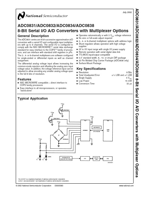
ADC12DC080资料

ADVANCE INFORMATIONSeptember 2007 ADC12DC080/ADC12DC105Dual 12-Bit, 80/105 MSPS A/D Converter with CMOS OutputsGeneral DescriptionNOTE: This is Advance Information for products current-ly in development. ALL specifications are design targets and are subject to change.The ADC12DC080 and ADC12DC105 are high-performance CMOS analog-to-digital converters capable of converting two analog input signals into 12-bit digital words at rates up to 80/105 Mega Samples Per Second (MSPS) respectively. These converters use a differential, pipelined architecture with digital error correction and an on-chip sample-and-hold circuit to minimize power consumption and the external com-ponent count, while providing excellent dynamic perfor-mance. A unique sample-and-hold stage yields a full-power bandwidth of 1 GHz. The ADC12DC080/105 may be operated from a single +3.3V power supply. A power-down feature re-duces the power consumption to very low levels while still allowing fast wake-up time to full operation. The differential inputs provide a 2V full scale differential input swing. A stable 1.2V internal voltage reference is provided, or the AD-C12DC080/105 can be operated with an external 1.2V refer-ence. Output data format (offset binary versus 2's comple-ment) and duty cycle stabilizer are pin-selectable. The duty cycle stabilizer maintains performance over a wide range of clock duty cycles.The ADC12DC080/105 is available in a 60-lead LLP package and operates over the industrial temperature range of −40°C to +85°C.Features■ 1 GHz Full Power Bandwidth■Internal sample-and-hold circuit and precision reference ■Low power consumption■Clock Duty Cycle Stabilizer■Single +3.3V supply operation■Power-down mode■Offset binary or 2's complement output data format■60-pin LLP package, (9x9x0.8mm, 0.5mm pin-pitch) Key Specifications■For ADC12DC105■Resolution12 Bits ■Conversion Rate105 MSPS ■SNR (f IN = 240 MHz)67 dBFS (typ)■SFDR (f IN = 240 MHz)83 dBFS (typ)■Full Power Bandwidth 1 GHz (typ)■Power Consumption800 mW (typ) Applications■High IF Sampling Receivers■Wireless Base Station Receivers■Test and Measurement Equipment■Communications Instrumentation■Portable InstrumentationConnection Diagram30015401© 2007 National Semiconductor ADC12DC080/ADC12DC105 Dual 12-Bit, 80/105 MSPS A/D Converter with CMOS OutputsBlock Diagram30015402Ordering InformationIndustrial (−40°C ≤ T A ≤ +85°C)Package ADC12DC080CISQ 60 Pin LLP ADC12DC105CISQ60 Pin LLP 2A D C 12D C 080/A D C 12D C 105Pin Descriptions and Equivalent CircuitsPin No.SymbolEquivalent CircuitDescriptionANALOG I/O313V IN A+V IN B+Differential analog input pins. The differential full-scale input signal level is 2V P-P with each input pin signal centered on a common mode voltage, V CM .214V IN A-V IN B-511V RP A V RP B These pins should each be bypassed to AGND with a low ESL (equivalent series inductance) 0.1 µF capacitor placed very close to the pin to minimize stray inductance. An 0201 size 0.1 µFcapacitor should be placed between V RP and V RN as close to the pins as possible, and a 1 µF capacitor should be placed in parallel.V RP and V RN should not be loaded. V CMO may be loaded to 1mA for use as a temperature stable 1.5V reference.It is recommended to use V CMO to provide the common mode voltage, V CM , for the differential analog inputs.79V CMO A V CMO B 610V RN A V RN B59V REFReference Voltage. This device provides an internally developed 1.2V reference. When using the internal reference, V REF should be decoupled to AGND with a 0.1 µF and a 1µF, low equivalent series inductance (ESL) capacitor.This pin may be driven with an external 1.2V reference voltage.This pin should not be used to source or sink current.DIGITAL I/O19OF/DCSThis is a four-state pin controlling the input clock mode and output data format.OF/DCS = V A , output data format is 2's complement without duty cycle stabilization applied to the input clockOF/DCS = AGND, output data format is offset binary, without duty cycle stabilization applied to the input clock.OF/DCS = (2/3)*V A , output data is 2's complement with duty cycle stabilization applied to the input clockOF/DCS = (1/3)*V A , output data is offset binary with duty cycle stabilization applied to the input clock.18CLKThe clock input pin.The analog inputs are sampled on the rising edge of the clock input.5720PD_A PD_BThis is a two-state input controlling Power Down.PD = V A , Power Down is enabled and power dissipation is reduced.PD = AGND, Normal operation.ADC12DC080/ADC12DC105Pin No.Symbol Equivalent CircuitDescription42-49,52-55DA0-DA7,DA8-DA11Digital data output pins that make up the 12-bit conversion result for Channel A. DA0 (pin 42) is the LSB, while DA11 (pin 55) is the MSB of the output word. Output levels are CMOS compatible.23-24,27-36DB0-DB1,DB3-DB11Digital data output pins that make up the 12-bit conversion result for Channel B. DB0 (pin 23) is the LSB, while DB11 (pin 36) is the MSB of the output word. Output levels are CMOS compatible.39DRDYData Ready Strobe. The data output transition is synchronized with the falling edge of this signal. This signal switches at the same frequency as the CLK input.ANALOG POWER 8, 16, 17, 58,60V APositive analog supply pins. These pins should be connected to a quiet source and be bypassed to AGND with 0.1 µF capacitors located close to the power pins.1, 4, 12, 15,Exposed Pad AGNDThe ground return for the analog supply.DIGITAL POWER 26, 38,50V DRPositive driver supply pin for the output drivers. This pin should be connected to a quiet voltage source and be bypassed to DRGND with a 0.1 µF capacitor located close to the power pin.25, 37, 51DRGNDThe ground return for the digital output driver supply. This pins should be connected to the system digital ground, but not be connected in close proximity to the ADC's AGND pins. 4A D C 12D C 080/A D C 12D C 105Absolute Maximum Ratings (Notes 1, 3)If Military/Aerospace specified devices are required,please contact the National Semiconductor Sales Office/Distributors for availability and specifications.Supply Voltage (V A , V DR )−0.3V to 4.2V Voltage on Any Pin (Not to exceed 4.2V)−0.3V to (V A +0.3V)Input Current at Any Pin other than Supply Pins (Note 4)±5 mA Package Input Current (Note 4)±50 mA Max Junction Temp (T J )+150°C Thermal Resistance (θJA )30°C/WESD Rating Human Body Model (Note 6)2500V Machine Model (Note 6)250V Storage Temperature −65°C to +150°C Soldering process must comply with National Semiconductor's Reflow Temperature Profilespecifications. Refer to /packaging.(Note 7)Operating Ratings(Notes 1, 3)Operating Temperature −40°C ≤ T A ≤ +85°CSupply Voltage (V A )+2.7V to +3.6V Output Driver Supply (V DR )+2.4V to V AClock Duty Cycle(DCS Enabled)30/70 %(DCS disabled)45/55 %V CM1.4V to 1.6V|AGND-DRGND|≤100mVADC12DC080 Converter Electrical CharacteristicsThis product is currently under development. As such, the parameters specified are DESIGN TARGETS. The specifica-tions cannot be guaranteed until device characterization has taken place.Unless otherwise specified, the following specifications apply: AGND = DRGND = 0V, V A = +3.0V, V DR = +2.5V, Internal V REF =+1.2V, f CLK = 80 MHz, V CM = V CMO , C L = 5 pF/pin. Typical values are for T A = 25°C. Boldface limits apply for T MIN ≤ T A ≤T MAX . All other limits apply for T A = 25°C (Notes 8, 9)SymbolParameterConditionsTypical (Note 10)LimitsUnits (Limits)STATIC CONVERTER CHARACTERISTICSResolution with No Missing Codes 12Bits (min)INL Integral Non Linearity (Note 11) ±0.5LSB (max)LSB (min)DNL Differential Non Linearity ±0.4LSB (max)LSB (min)Under Range Output Code 00Over Range Output Code40954095 REFERENCE AND ANALOG INPUT CHARACTERISTICS V CMO Common Mode Output Voltage 1.5 1.451.55V (min)V (max)V CM Analog Input Common Mode Voltage1.5 1.41.6V (min)V (max)C IN V IN Input Capacitance (each pin to GND) (Note 12)V IN = 1.5 Vdc ± 0.5 V (CLK LOW)8.5 pF (CLK HIGH)3.5 pF V REFExternal Reference Voltage1.201.1761.224V (min)V (max)ADC12DC080/ADC12DC105ADC12DC080 Dynamic Converter Electrical CharacteristicsUnless otherwise specified, the following specifications apply: AGND = DRGND = 0V, V A = +3.0V, V DR = +2.5V, Internal V REF =+1.2V, f CLK = 80 MHz, V CM = V CMO , C L = 5 pF/pin, . Typical values are for T A = 25°C. Boldface limits apply for T MIN ≤ T A ≤T MAX . All other limits apply for T A = 25°C (Notes 8, 9)SymbolParameterConditionsTypical(Note 10)LimitsUnits (Limits)(Note 2)DYNAMIC CONVERTER CHARACTERISTICS, A IN = -1dBFS FPBW Full Power Bandwidth -1 dBFS Input, −3 dB Corner1.0 GHz SNRSignal-to-Noise Ratiof IN = 10 MHz 71.2dBFS f IN = 70 MHz 70dBFSf IN = 170 MHz 68 dBFS SFDRSpurious Free Dynamic Rangef IN = 10 MHz90 dBFS f IN = 70 MHz 88dBFS f IN = 170 MHz 83 dBFS ENOBEffective Number of Bitsf IN = 10 MHz11.5 Bits f IN = 70 MHz 11.3Bits f IN = 170 MHz 11 Bits THDTotal Harmonic Disortionf IN = 10 MHz−88 dBFS f IN = 70 MHz −85dBFS f IN = 170 MHz −80 dBFS H2Second Harmonic Distortionf IN = 10 MHz−100 dBFS f IN = 70 MHz −95dBFS f IN = 170 MHz −85 dBFS H3Third Harmonic Distortionf IN = 10 MHz−90 dBFS f IN = 70 MHz −88dBFS f IN = 170 MHz −83 dBFS SINADSignal-to-Noise and Distortion Ratiof IN = 10 MHz71.1 dBFS f IN = 70 MHz 69.8dBFS f IN = 170 MHz67.7dBFSADC12DC080 Logic and Power Supply Electrical CharacteristicsUnless otherwise specified, the following specifications apply: AGND = DRGND = 0V, V A = +3.0V, V DR = +2.5V, Internal V REF =+1.2V, f CLK = 80 MHz, V CM = V CMO , C L = 5 pF/pin. Typical values are for T A = 25°C. Boldface limits apply for T MIN ≤ T A ≤T MAX . All other limits apply for T A = 25°C (Notes 8, 9)SymbolParameterConditionsTypical (Note 10)LimitsUnits (Limits)DIGITAL INPUT CHARACTERISTICS (CLK, PD_A,PD_B)V IN(1)Logical “1” Input Voltage V D = 3.6V 2.0V (min)V IN(0)Logical “0” Input Voltage V D = 3.0V 0.8V (max)I IN(1)Logical “1” Input Current V IN = 3.3V 10 µA I IN(0)Logical “0” Input Current V IN = 0V −10 µA C IN Digital Input Capacitance5 pF DIGITAL OUTPUT CHARACTERISTICS (DA0-DA11,DB0-DB11,DRDY)V OUT(1)Logical “1” Output Voltage I OUT = −0.5 mA , V DR = 2.4V 1.2V (min)V OUT(0)Logical “0” Output VoltageI OUT = 1.6 mA, V DR = 2.4V 0.4V (max)+I SC Output Short Circuit Source Current V OUT = 0V −10 mA −I SC Output Short Circuit Sink Current V OUT = V DR 10 mA C OUTDigital Output Capacitance5pFPOWER SUPPLY CHARACTERISTICS 6A D C 12D C 080/A D C 12D C 105Symbol Parameter ConditionsTypical(Note 10)LimitsUnits(Limits)IAAnalog Supply Current Full Operation200mA (max)IDRDigital Output Supply Current Full Operation (Note 13)26mAPower Consumption Excludes I DR (Note 13)600mW (max) Power Down Power Consumption PD_A=PD_B=V A30mW ADC12DC080 Timing and AC CharacteristicsUnless otherwise specified, the following specifications apply: AGND = DRGND = 0V, VA = +3.0V, VDR= +2.5V, Internal VREF=+1.2V, fCLK = 80 MHz, VCM= VCMO, CL= 5 pF/pin. Typical values are for TA= 25°C. Timing measurements are taken at 50% ofthe signal amplitude. Boldface limits apply for TMIN ≤ TA≤ TMAX. All other limits apply for TA= 25°C (Notes 8, 9)Symb Parameter ConditionsTypical(Note 10)LimitsUnits(Limits)Maximum Clock Frequency80MHz (max) Minimum Clock Frequency20MHz (min) tCHClock High Time6nstCLClock Low Time6nstCONVConversion Latency7Clock Cyclest OD Output Delay of CLK to DATA Relative to rising edge of CLK426ns (min)ns (max)tSUData Output Setup Time Relative to DRDY5ns (min)tHData Output Hold Time Relative to DRDY5ns (min)tADAperture Delay0.6nstAJAperture Jitter0.1ps rmsADC12DC080/ADC12DC105ADC12DC105 Converter Electrical CharacteristicsThis product is currently under development. As such, the parameters specified are DESIGN TARGETS. The specifica-tions cannot be guaranteed until device characterization has taken place.Unless otherwise specified, the following specifications apply: AGND = DRGND = 0V, V A = +3.3V, V DR = +2.5V, Internal V REF =+1.2V, f CLK = 105 MHz, V CM = V CMO , C L = 5 pF/pin. Typical values are for T A = 25°C. Boldface limits apply for T MIN ≤ T A ≤T MAX . All other limits apply for T A = 25°C (Notes 8, 9)SymbolParameterConditionsTypical(Note 10)LimitsUnits (Limits)STATIC CONVERTER CHARACTERISTICSResolution with No Missing Codes 12Bits (min)INL Integral Non Linearity (Note 11) ±0.5LSB (max)LSB (min)DNL Differential Non Linearity ±0.4LSB (max)LSB (min)Under Range Output Code 00Over Range Output Code40954095 REFERENCE AND ANALOG INPUT CHARACTERISTICS V CMO Common Mode Output Voltage 1.5 1.451.55V (min)V (max)V CM Analog Input Common Mode Voltage1.5 1.41.6V (min)V (max)C IN V IN Input Capacitance (each pin to GND)(Note 12)V IN = 1.5 Vdc ± 0.5 V (CLK LOW)8.5 pF (CLK HIGH)3.5 pF V REFExternal Reference Voltage1.201.1761.224V (min)V (max)ADC12DC105 Dynamic Converter Electrical CharacteristicsUnless otherwise specified, the following specifications apply: AGND = DRGND = 0V, V A = +3.3V, V DR = +2.5V, Internal V REF =+1.2V, f CLK = 105 MHz, V CM = V CMO , C L = 5 pF/pin, . Typical values are for T A = 25°C. Boldface limits apply for T MIN ≤ T A ≤T MAX . All other limits apply for T A = 25°C (Notes 8, 9)SymbolParameterConditionsTypical(Note 10)LimitsUnits (Limits)(Note 2)DYNAMIC CONVERTER CHARACTERISTICS, A IN = -1dBFS FPBW Full Power Bandwidth -1 dBFS Input, −3 dB Corner1.0 GHz SNRSignal-to-Noise Ratiof IN = 10 MHz 70.1dBFS f IN = 70 MHz 69.1dBFSf IN = 240 MHz 67 dBFS SFDRSpurious Free Dynamic Rangef IN = 10 MHz88 dBFS f IN = 70 MHz 85dBFS f IN = 240 MHz 83 dBFS ENOBEffective Number of Bitsf IN = 10 MHz11.3 Bits f IN = 70 MHz 11.2Bits f IN = 240 MHz 10.8 Bits THDTotal Harmonic Disortionf IN = 10 MHz−86 dBFS f IN = 70 MHz −85dBFS f IN = 240 MHz −80 dBFS H2Second Harmonic Distortionf IN = 10 MHz−95 dBFS f IN = 70 MHz −90dBFS f IN = 240 MHz−85dBFS 8A D C 12D C 080/A D C 12D C 105Symbol Parameter ConditionsTypical(Note 10)LimitsUnits(Limits)(Note 2)H3Third Harmonic DistortionfIN= 10 MHz−88dBFSfIN= 70 MHz−85dBFSfIN= 240 MHz−83dBFSSINAD Signal-to-Noise and Distortion RatiofIN= 10 MHz70dBFSfIN= 70 MHz69dBFSfIN= 240 MHz66.8dBFSADC12DC105 Logic and Power Supply Electrical CharacteristicsUnless otherwise specified, the following specifications apply: AGND = DRGND = 0V, VA = +3.3V, VDR= +2.5V, Internal VREF=+1.2V, fCLK = 105 MHz, VCM= VCMO, CL= 5 pF/pin. Typical values are for TA= 25°C. Boldface limits apply for TMIN≤ TA≤T MAX . All other limits apply for TA= 25°C (Notes 8, 9)Symbol Parameter ConditionsTypical(Note 10)LimitsUnits(Limits)DIGITAL INPUT CHARACTERISTICS (CLK, PD_A,PD_B)VIN(1)Logical “1” Input Voltage V D = 3.6V 2.0V (min)VIN(0)Logical “0” Input Voltage V D = 3.0V0.8V (max)IIN(1)Logical “1” Input Current V IN = 3.3V10µAIIN(0)Logical “0” Input Current VIN= 0V−10µACINDigital Input Capacitance5pFDIGITAL OUTPUT CHARACTERISTICS (DA0-DA11,DB0-DB11,DRDY)VOUT(1)Logical “1” Output Voltage I OUT = −0.5 mA , V DR = 2.4V 1.2V (min)VOUT(0)Logical “0” Output Voltage I OUT = 1.6 mA, V DR = 2.4V0.4V (max)+ISC Output Short Circuit Source Current VOUT= 0V−10mA−ISCOutput Short Circuit Sink Current V OUT = V DR10mACOUTDigital Output Capacitance5pF POWER SUPPLY CHARACTERISTICSIAAnalog Supply Current Full Operation242mA (max)IDRDigital Output Supply Current Full Operation (Note 13)32mAPower Consumption Excludes I DR (Note 13)800mW (max) Power Down Power Consumption PD_A=PD_B=V A33mW ADC12DC105 Timing and AC CharacteristicsUnless otherwise specified, the following specifications apply: AGND = DRGND = 0V, VA = +3.3V, VDR= +2.5V, Internal VREF=+1.2V, fCLK = 105 MHz, VCM= VCMO, CL= 5 pF/pin. Typical values are for TA= 25°C. Timing measurements are taken at 50% ofthe signal amplitude. Boldface limits apply for TMIN ≤ TA≤ TMAX. All other limits apply for TA= 25°C (Notes 8, 9)Symb Parameter ConditionsTypical(Note 10)LimitsUnits(Limits)Maximum Clock Frequency105MHz (max) Minimum Clock Frequency20MHz (min) tCHClock High Time4nstCLClock Low Time4nstCONVConversion Latency7Clock Cyclest OD Output Delay of CLK to DATA Relative to rising edge of CLK426ns (min)ns (max)tSUData Output Setup Time Relative to DRDY3ns (min)tHData Output Hold Time Relative to DRDY3ns (min)tADAperture Delay0.6nstAJAperture Jitter0.1ps rmsADC12DC080/ADC12DC105Note 1:Absolute Maximum Ratings indicate limits beyond which damage to the device may occur. Operating Ratings indicate conditions for which the device is guaranteed to be functional, but do not guarantee specific performance limits. For guaranteed specifications and test conditions, see the Electrical Characteristics.The guaranteed specifications apply only for the test conditions listed. Some performance characteristics may degrade when the device is not operated under the listed test conditions. Operation of the device beyond the maximum Operating Ratings is not recommended.Note 2:This parameter is specified in units of dBFS - indicating the value that would be attained with a full-scale input signal.Note 3:All voltages are measured with respect to GND = AGND = DRGND = 0V, unless otherwise specified.Note 4:When the input voltage at any pin exceeds the power supplies (that is, V IN < AGND, or V IN > V A ), the current at that pin should be limited to ±5 mA. The ±50 mA maximum package input current rating limits the number of pins that can safely exceed the power supplies with an input current of ±5 mA to 10.Note 5:The maximum allowable power dissipation is dictated by T J,max , the junction-to-ambient thermal resistance, (θJA ), and the ambient temperature, (T A ), and can be calculated using the formula P D,max = (T J,max - T A )/θJA . The values for maximum power dissipation listed above will be reached only when the device is operated in a severe fault condition (e.g. when input or output pins are driven beyond the power supply voltages, or the power supply polarity is reversed). Such conditions should always be avoided.Note 6:Human Body Model is 100 pF discharged through a 1.5 k Ω resistor. Machine Model is 220 pF discharged through 0 ΩNote 7:Reflow temperature profiles are different for lead-free and non-lead-free packages.Note 8:The inputs are protected as shown below. Input voltage magnitudes above V A or below GND will not damage this device, provided current is limited per (Note 4). However, errors in the A/D conversion can occur if the input goes above 2.6V or below GND as described in the Operating Ratings section.30015411Note 9:With a full scale differential input of 2V P-P , the 12-bit LSB is 488 µV.Note 10:Typical figures are at T A = 25°C and represent most likely parametric norms at the time of product characterization. The typical specifications are not guaranteed.Note 11:Integral Non Linearity is defined as the deviation of the analog value, expressed in LSBs, from the straight line that passes through positive and negative full-scale.Note 12:The input capacitance is the sum of the package/pin capacitance and the sample and hold circuit capacitance.Note 13:I DR is the current consumed by the switching of the output drivers and is primarily determined by load capacitance on the output pins, the supply voltage,V DR , and the rate at which the outputs are switching (which is signal dependent). I DR =V DR (C 0 x f 0 + C 1 x f 1 +....C 11 x f 11) where V DR is the output driver power supply voltage, C n is total capacitance on the output pin, and f n is the average frequency at which that pin is toggling.Note 14:This parameter is guaranteed by design and/or characterization and is not tested in production. 10A D C 12D C 080/A D C 12D C 105Specification DefinitionsAPERTURE DELAY is the time after the falling edge of the clock to when the input signal is acquired or held for conver-sion.APERTURE JITTER (APERTURE UNCERTAINTY) is the variation in aperture delay from sample to sample. Aperture jitter manifests itself as noise in the output.CLOCK DUTY CYCLE is the ratio of the time during one cycle that a repetitive digital waveform is high to the total time of one period. The specification here refers to the ADC clock input signal.COMMON MODE VOLTAGE (V CM ) is the common DC volt-age applied to both input terminals of the ADC.CONVERSION LATENCY is the number of clock cycles be-tween initiation of conversion and when that data is presented to the output driver stage. Data for any given sample is avail-able at the output pins the Pipeline Delay plus the Output Delay after the sample is taken. New data is available at every clock cycle, but the data lags the conversion by the pipeline delay.CROSSTALK is coupling of energy from one channel into the other channel.DIFFERENTIAL NON-LINEARITY (DNL) is the measure of the maximum deviation from the ideal step size of 1 LSB.EFFECTIVE NUMBER OF BITS (ENOB, or EFFECTIVE BITS) is another method of specifying Signal-to-Noise and Distortion Ratio or SINAD. ENOB is defined as (SINAD -1.76) / 6.02 and says that the converter is equivalent to a perfect ADC of this (ENOB) number of bits.FULL POWER BANDWIDTH is a measure of the frequency at which the reconstructed output fundamental drops 3 dB below its low frequency value for a full scale input.GAIN ERROR is the deviation from the ideal slope of the transfer function. It can be calculated as:Gain Error = Positive Full Scale Error − Negative Full ScaleError It can also be expressed as Positive Gain Error and Negative Gain Error, which are calculated as:PGE = Positive Full Scale Error - Offset Error NGE = Offset Error - Negative Full Scale ErrorINTEGRAL NON LINEARITY (INL) is a measure of the de-viation of each individual code from a best fit straight line. The deviation of any given code from this straight line is measured from the center of that code value.INTERMODULATION DISTORTION (IMD) is the creation of additional spectral components as a result of two sinusoidal frequencies being applied to the ADC input at the same time.It is defined as the ratio of the power in the intermodulation products to the total power in the original frequencies. IMD is usually expressed in dBFS.LSB (LEAST SIGNIFICANT BIT) is the bit that has the small-est value or weight of all bits. This value is V FS /2n , where “V FS ” is the full scale input voltage and “n” is the ADC reso-lution in bits.MISSING CODES are those output codes that will never ap-pear at the ADC outputs. The ADC is guaranteed not to have any missing codes.MSB (MOST SIGNIFICANT BIT) is the bit that has the largest value or weight. Its value is one half of full scale.NEGATIVE FULL SCALE ERROR is the difference between the actual first code transition and its ideal value of ½ LSB above negative full scale.OFFSET ERROR is the difference between the two input voltages [(V IN +) – (V IN -)] required to cause a transition from code 2047 to 2048.OUTPUT DELAY is the time delay after the falling edge of the clock before the data update is presented at the output pins.PIPELINE DELAY (LATENCY) See CONVERSION LATEN-CY.POSITIVE FULL SCALE ERROR is the difference between the actual last code transition and its ideal value of 1½ LSB below positive full scale.POWER SUPPLY REJECTION RATIO (PSRR) is a measure of how well the ADC rejects a change in the power supply voltage. PSRR is the ratio of the Full-Scale output of the ADC with the supply at the minimum DC supply limit to the Full-Scale output of the ADC with the supply at the maximum DC supply limit, expressed in dB.SIGNAL TO NOISE RATIO (SNR) is the ratio, expressed in dB, of the rms value of the input signal to the rms value of the sum of all other spectral components below one-half the sam-pling frequency, not including harmonics or DC.SIGNAL TO NOISE PL US DISTORTION (S/N+D or SINAD) Is the ratio, expressed in dB, of the rms value of the input signal to the rms value of all of the other spectral com-ponents below half the clock frequency, including harmonics but excluding d.c.SPURIOUS FREE DYNAMIC RANGE (SFDR) is the differ-ence, expressed in dB, between the rms values of the input signal and the peak spurious signal, where a spurious signal is any signal present in the output spectrum that is not present at the input.TOTAL HARMONIC DISTORTION (THD) is the ratio, ex-pressed in dB, of the rms total of the first nine harmonic levels at the output to the level of the fundamental at the output. THD is calculated aswhere f 1 is the RMS power of the fundamental (output) fre-quency and f 2 through f 10 are the RMS power of the first 9harmonic frequencies in the output spectrum.SECOND HARMONIC DISTORTION (2ND HARM) is the dif-ference expressed in dB, between the RMS power in the input frequency at the output and the power in its 2nd harmonic level at the output.THIRD HARMONIC DISTORTION (3RD HARM) is the dif-ference, expressed in dB, between the RMS power in the input frequency at the output and the power in its 3rd harmonic level at the output.ADC12DC080/ADC12DC105Timing Diagrams30015409FIGURE 1. Output TimingTransfer Characteristic30015410FIGURE 2. Transfer Characteristic 12A D C 12D C 080/A D C 12D C 105Physical Dimensions inches (millimeters) unless otherwise notedTOP View...............................SIDE View...............................BOTTOM View60-Lead LLP PackageOrdering Numbers:ADC12DC080CISQ / ADC12DC105CISQNS Package Number SQA60A ADC12DC080/ADC12DC105NotesA D C 12D C 080/A D C 12D C 105 D u a l 12-B i t , 80/105 M S P S A /DC o n v e r t e r w i t h C M O S O u t p u t sTHE CONTENTS OF THIS DOCUMENT ARE PROVIDED IN CONNECTION WITH NATIONAL SEMICONDUCTOR CORPORATION (“NATIONAL”) PRODUCTS. NATIONAL MAKES NO REPRESENTATIONS OR WARRANTIES WITH RESPECT TO THE ACCURACY OR COMPLETENESS OF THE CONTENTS OF THIS PUBLICATION AND RESERVES THE RIG HT TO MAKE CHANG ES TO SPECIFICATIONS AND PRODUCT DESCRIPTIONS AT ANY TIME WITHOUT NOTICE. NO LICENSE, WHETHER EXPRESS,IMPLIED, ARISING BY ESTOPPEL OR OTHERWISE, TO ANY INTELLECTUAL PROPERTY RIG HTS IS G RANTED BY THIS DOCUMENT.TESTING AND OTHER QUALITY CONTROLS ARE USED TO THE EXTENT NATIONAL DEEMS NECESSARY TO SUPPORT NATIONAL’S PRODUCT WARRANTY. EXCEPT WHERE MANDATED BY G OVERNMENT REQUIREMENTS, TESTING OF ALL PARAMETERS OF EACH PRODUCT IS NOT NECESSARILY PERFORMED. NATIONAL ASSUMES NO LIABILITY FOR APPLICATIONS ASSISTANCE OR BUYER PRODUCT DESIG N. BUYERS ARE RESPONSIBLE FOR THEIR PRODUCTS AND APPLICATIONS USING NATIONAL COMPONENTS. PRIOR TO USING OR DISTRIBUTING ANY PRODUCTS THAT INCLUDE NATIONAL COMPONENTS, BUYERS SHOULD PROVIDE ADEQUATE DESIGN, TESTING AND OPERATING SAFEGUARDS.EXCEPT AS PROVIDED IN NATIONAL’S TERMS AND CONDITIONS OF SALE FOR SUCH PRODUCTS, NATIONAL ASSUMES NO LIABILITY WHATSOEVER, AND NATIONAL DISCLAIMS ANY EXPRESS OR IMPLIED WARRANTY RELATING TO THE SALE AND/OR USE OF NATIONAL PRODUCTS INCLUDING LIABILITY OR WARRANTIES RELATING TO FITNESS FOR A PARTICULAR PURPOSE, MERCHANTABILITY, OR INFRING EMENT OF ANY PATENT, COPYRIG HT OR OTHER INTELLECTUAL PROPERTY RIGHT.LIFE SUPPORT POLICYNATIONAL ’S PRODUCTS ARE NOT AUTHORIZED FOR USE AS CRITICAL COMPONENTS IN L IFE SUPPORT DEVICES OR SYSTEMS WITHOUT THE EXPRESS PRIOR WRITTEN APPROVAL OF THE CHIEF EXECUTIVE OFFICER AND GENERAL COUNSEL OF NATIONAL SEMICONDUCTOR CORPORATION. As used herein:Life support devices or systems are devices which (a) are intended for surgical implant into the body, or (b) support or sustain life and whose failure to perform when properly used in accordance with instructions for use provided in the labeling can be reasonably expected to result in a significant injury to the user. A critical component is any component in a life support device or system whose failure to perform can be reasonably expected to cause the failure of the life support device or system or to affect its safety or effectiveness.National Semiconductor and the National Semiconductor logo are registered trademarks of National Semiconductor Corporation. All other brand or product names may be trademarks or registered trademarks of their respective holders.Copyright© 2007 National Semiconductor CorporationFor the most current product information visit us at National Semiconductor Americas Customer Support Center Email:new.feedback@ Tel: 1-800-272-9959National Semiconductor Europe Customer Support Center Fax: +49 (0) 180-530-85-86Email: europe.support@ Deutsch Tel: +49 (0) 69 9508 6208English Tel: +49 (0) 870 24 0 2171Français Tel: +33 (0) 1 41 91 8790National Semiconductor Asia Pacific Customer Support Center Email: ap.support@National Semiconductor Japan Customer Support Center Fax: 81-3-5639-7507Email: jpn.feedback@ Tel: 81-3-5639-7560。
常用ic名称
74系列TTL电路检索7400 TTL 2输入端四与非门7401 TTL 集电极开路2输入端四与非门7402 TTL 2输入端四或非门7403 TTL 集电极开路2输入端四与非门7404 TTL 六反相器7405 TTL 集电极开路六反相器7406 TTL 集电极开路六反相高压驱动器7407 TTL 集电极开路六正相高压驱动器7408 TTL 2输入端四与门7409 TTL 集电极开路2输入端四与门7410 TTL 3输入端3与非门74107 TTL 带清除主从双J-K触发器74109 TTL 带预置清除正触发双J-K触发器7411 TTL 3输入端3与门74112 TTL 带预置清除负触发双J-K触发器7412 TTL 开路输出3输入端三与非门74121 TTL 单稳态多谐振荡器74122 TTL 可再触发单稳态多谐振荡器74123 TTL 双可再触发单稳态多谐振荡器74125 TTL 三态输出高有效四总线缓冲门74126 TTL 三态输出低有效四总线缓冲门7413 TTL 4输入端双与非施密特触发器74132 TTL 2输入端四与非施密特触发器74133 TTL 13输入端与非门74136 TTL 四异或门74138 TTL 3-8线译码器/复工器74139 TTL 双2-4线译码器/复工器7414 TTL 六反相施密特触发器74145 TTL BCD—十进制译码/驱动器7415 TTL 开路输出3输入端三与门74150 TTL 16选1数据选择/多路开关74151 TTL 8选1数据选择器74153 TTL 双4选1数据选择器74154 TTL 4线—16线译码器74155 TTL 图腾柱输出译码器/分配器74156 TTL 开路输出译码器/分配器74157 TTL 同相输出四2选1数据选择器74158 TTL 反相输出四2选1数据选择器7416 TTL 开路输出六反相缓冲/驱动器74160 TTL 可预置BCD异步清除计数器74161 TTL 可予制四位二进制异步清除计数器74162 TTL 可预置BCD同步清除计数器74163 TTL 可予制四位二进制同步清除计数器74164 TTL 八位串行入/并行输出移位寄存器74165 TTL 八位并行入/串行输出移位寄存器74166 TTL 八位并入/串出移位寄存器74169 TTL 二进制四位加/减同步计数器7417 TTL 开路输出六同相缓冲/驱动器74170 TTL 开路输出4×4寄存器堆74173 TTL 三态输出四位D型寄存器74174 TTL 带公共时钟和复位六D触发器74175 TTL 带公共时钟和复位四D触发器74180 TTL 9位奇数/偶数发生器/校验器74181 TTL 算术逻辑单元/函数发生器74185 TTL 二进制—BCD代码转换器74190 TTL BCD同步加/减计数器74191 TTL 二进制同步可逆计数器74192 TTL 可预置BCD双时钟可逆计数器74193 TTL 可预置四位二进制双时钟可逆计数器74194 TTL 四位双向通用移位寄存器74195 TTL 四位并行通道移位寄存器74196 TTL 十进制/二-十进制可预置计数锁存器74197 TTL 二进制可预置锁存器/计数器7420 TTL 4输入端双与非门7421 TTL 4输入端双与门7422 TTL 开路输出4输入端双与非门74221 TTL 双/单稳态多谐振荡器74240 TTL 八反相三态缓冲器/线驱动器74241 TTL 八同相三态缓冲器/线驱动器74243 TTL 四同相三态总线收发器74244 TTL 八同相三态缓冲器/线驱动器74245 TTL 八同相三态总线收发器74247 TTL BCD—7段15V输出译码/驱动器74248 TTL BCD—7段译码/升压输出驱动器74249 TTL BCD—7段译码/开路输出驱动器74251 TTL 三态输出8选1数据选择器/复工器74253 TTL 三态输出双4选1数据选择器/复工器74256 TTL 双四位可寻址锁存器74257 TTL 三态原码四2选1数据选择器/复工器74258 TTL 三态反码四2选1数据选择器/复工器74259 TTL 八位可寻址锁存器/3-8线译码器7426 TTL 2输入端高压接口四与非门74260 TTL 5输入端双或非门74266 TTL 2输入端四异或非门7427 TTL 3输入端三或非门74273 TTL 带公共时钟复位八D触发器74279 TTL 四图腾柱输出S-R锁存器7428 TTL 2输入端四或非门缓冲器74283 TTL 4位二进制全加器74290 TTL 二/五分频十进制计数器74293 TTL 二/八分频四位二进制计数器74295 TTL 四位双向通用移位寄存器74298 TTL 四2输入多路带存贮开关74299 TTL 三态输出八位通用移位寄存器7430 TTL 8输入端与非门7432 TTL 2输入端四或门74322 TTL 带符号扩展端八位移位寄存器74323 TTL 三态输出八位双向移位/存贮寄存器7433 TTL 开路输出2输入端四或非缓冲器74347 TTL BCD—7段译码器/驱动器74352 TTL 双4选1数据选择器/复工器74353 TTL 三态输出双4选1数据选择器/复工器74365 TTL 门使能输入三态输出六同相线驱动器74366 TTL 门使能输入三态输出六反相线驱动器74367 TTL 4/2线使能输入三态六同相线驱动器74368 TTL 4/2线使能输入三态六反相线驱动器7437 TTL 开路输出2输入端四与非缓冲器74373 TTL 三态同相八D锁存器74374 TTL 三态反相八D锁存器74375 TTL 4位双稳态锁存器74377 TTL 单边输出公共使能八D锁存器74378 TTL 单边输出公共使能六D锁存器74379 TTL 双边输出公共使能四D锁存器7438 TTL 开路输出2输入端四与非缓冲器74380 TTL 多功能八进制寄存器7439 TTL 开路输出2输入端四与非缓冲器74390 TTL 双十进制计数器74393 TTL 双四位二进制计数器7440 TTL 4输入端双与非缓冲器7442 TTL BCD—十进制代码转换器74447 TTL BCD—7段译码器/驱动器7445 TTL BCD—十进制代码转换/驱动器74450 TTL 16:1多路转接复用器多工器74451 TTL 双8:1多路转接复用器多工器74453 TTL 四4:1多路转接复用器多工器7446 TTL BCD—7段低有效译码/驱动器74460 TTL 十位比较器74461 TTL 八进制计数器74465 TTL 三态同相2与使能端八总线缓冲器74466 TTL 三态反相2与使能八总线缓冲器74467 TTL 三态同相2使能端八总线缓冲器74468 TTL 三态反相2使能端八总线缓冲器74469 TTL 八位双向计数器7447 TTL BCD—7段高有效译码/驱动器7448 TTL BCD—7段译码器/内部上拉输出驱动74490 TTL 双十进制计数器74491 TTL 十位计数器74498 TTL 八进制移位寄存器7450 TTL 2-3/2-2输入端双与或非门74502 TTL 八位逐次逼近寄存器74503 TTL 八位逐次逼近寄存器7451 TTL 2-3/2-2输入端双与或非门74533 TTL 三态反相八D锁存器74534 TTL 三态反相八D锁存器7454 TTL 四路输入与或非门74540 TTL 八位三态反相输出总线缓冲器7455 TTL 4输入端二路输入与或非门74563 TTL 八位三态反相输出触发器74564 TTL 八位三态反相输出D触发器74573 TTL 八位三态输出触发器74574 TTL 八位三态输出D触发器74645 TTL 三态输出八同相总线传送接收器74670 TTL 三态输出4×4寄存器堆7473 TTL 带清除负触发双J-K触发器7474 TTL 带置位复位正触发双D触发器7476 TTL 带预置清除双J-K触发器7483 TTL 四位二进制快速进位全加器7485 TTL 四位数字比较器7486 TTL 2输入端四异或门7490 TTL 可二/五分频十进制计数器7493 TTL 可二/八分频二进制计数器7495 TTL 四位并行输入\输出移位寄存器7497 TTL 6位同步二进制乘法器ICL7106,ICL7107 3位半A/D转换器DAC0830/DAC0832 8位D/A转换器ADC0831/ADC0832/ADC0834/ADC0838 8位A/D转换器ADC0808/ADC0809 8位A/D转换器ADC0802/ADC0803/ADC0804 8位A/D转换器AD7520/AD7521/AD7530/AD7521 D/A转换器4N35/4N36/4N37 光电耦合器ICL7116,ICL7117 3位半A/D转换器ICL7650 载波稳零运算放大器ICL7660/MAX1044 CMOS电源电压变换器ICL8038 单片函数发生器ICM7216 10MHz通用计数器ICM7226 带BCD输出10MHz通用计数器ISO2-CMOS MT8880C DTMF 收发器LF351 JFET输入运算放大器LF353 JFET输入宽带高速双运算放大器LM117/LM317A/LM317 三端可调电源LM124/LM124/LM324 低功耗四运算放大器LM137/LM337 三端可调负电压调整器LM139/LM239/LM339 低功耗四电压比较器LM158/LM258/LM358 低功耗双运算放大器LM193/LM293/LM393 低功耗双电压比较器LM201/LM301 通用运算放大器[中文资料]LM231/LM331 精密电压—频率转换器LM285/LM385 微功耗基准电压二极管[中文资料]LM308A 精密运算放大器LM386 低压音频小功率放大器LM399 带温度稳定器精密电压基准电路LM431 可调电压基准电路LM567/LM567C 锁相环音频译码器LM741 运算放大器LM831 双低噪声音频功率放大器LM833 双低噪声音频放大器LM8365 双定时LED电子钟电路MAX038 0.1Hz-20MHz 单片函数发生器MAX232 5V电源多通道RS232驱动器/接收器MC1403 2.5V精密电压基准电路MC1404 5.0v/6.25v/10v 基准电压MC1413/MC1416 七路达林顿驱动器MC145026/MC145027/MC145028 编码器/译码器MC145403-5/8 RS232驱动器/接收器MC145406 RS232驱动器/接收器MC145407 RS232驱动器/接收器MC145583 RS232驱动器/接收器MC145740 DTMF 接收器MC1488 二输入与非四线路驱动器MC1489 四施密特可控线路驱动器MC2833 低功率调频发射系统MC3362 低功率调频窄频带接收器MC4558 双运算放大器MC7800系列1.0A三端正电压稳压器MC78L00系列0.1A三端正电压稳压器[中文资料]MC78M00系列0.5A三端正电压稳压器MC78T00系列3.0A正电压稳压器[中文资料]MC7900系列1.0A三端负电压稳压器[中文资料]MC79L00系列0.1A三端负电压稳压器[中文资料]MC79M00系列0.5A三端负电压稳压器[中文资料]Microchip PIC系列单片机RS232通讯应用MM5369 3.579545MHz-60Hz 17级分频振荡器MOC3009/MOC3012 双向可控硅输出光电耦合器MOC3020/MOC3023 双向可控硅输出光电耦合器MOC3081/MOC3082/MOC3083 过零双向可控硅输出光电耦合器MOC8050 无基极达林顿晶体管输出光电耦合器MOC8111 无基极晶体管输出光电耦合器MT8870 DTMF双音频接收器MT8888C DTMF 收发器NE5532/NE5532A 双低噪声运算放大器NE5534/SE5534 低噪声运算放大器NE555/SA555 单时基电路NE556/SA556/SE556 双时基电路NE570/NE571/SA571 音频压缩扩展器OP07 低电压飘移运算放大器OP27 低噪音精密运算放大器OP37 低噪音高速精密运算放大器OP77 低电压飘移运算放大器OP90 精密低电压微功耗运算放大器PC817/PC827/PC847 高效光电耦合器PT2262 无线遥控发射编码器芯片PT2272 无线遥控接收解码器芯片SG2524/SG3524 脉宽调制PWMST7537 电力线调制解调器电路TDA1521 2×12W Hi-Fi 音频功率放大器TDA2030 14W Hi-Fi 音频放大器TDA7000T FM 单片调频接收电路TDA7010T FM 单片调频接收电路TDA7021T FM MTS 单片调频接收电路TDA7040T 低电压锁相环立体声解码器TDA7050 低电压单/双声道功率放大器TL062/TL064 低功耗JFET输入运算放大器TL071/TL072/TL074 低噪声JFET输入运算放大器TL082/TL084 JFET 宽带高速运算放大器TL494 脉宽调制PWMTL594 精密开关模式脉宽调制控制TLP521/1-4 光电耦合器TOP100-4 TOPSwitch 三端PWM开关电源电路TOP221-7 TOPSwitch-Ⅱ三端PWM开关电源电路TOP232-4 TOPSwitch-FX 五端柔韧设计开关电源电路TOP412/TOP414 TOPSwitch 三端PWM DC-DC 开关电源ULN2068 1.5A/50V 4路达林顿驱动电路ULN2803 500mA/50V 8路达林顿驱动电路ULN2803/ULN2804 线性八外围驱动器阵列[中文资料] VFC32 电压—频率/频率—电压转换器添加评论40系列CMOS电路检索4000 CMOS 3输入双或非门1反相器4001 CMOS 四2输入或非门4002 CMOS 双4输入或非门4006 CMOS 18级静态移位寄存器4007 CMOS 双互补对加反相器4008 CMOS 4位二进制并行进位全加器4009 CMOS 六缓冲器/转换器(反相)4010 CMOS 六缓冲器/转换器(同相)40100 CMOS 32位双向静态移位寄存器40101 CMOS 9位奇偶发生器/校验器40102 CMOS 8位BCD可预置同步减法计数器40103 CMOS 8位二进制可预置同步减法计数器40104 CMOS 4位三态输出双向通用移位寄存器40105 CMOS 先进先出寄存器40106 CMOS 六施密特触发器40107 CMOS 2输入双与非缓冲/驱动器40108 CMOS 4×4多端寄存40109 CMOS 四三态输出低到高电平移位器4011 CMOS 四2输入与非门40110 CMOS 十进制加减计数/译码/锁存/驱动40117 CMOS 10线—4线BCD优先编码器4012 CMOS 双4输入与非门4013 CMOS 带置位/复位的双D触发器4014 CMOS 8级同步并入串入/串出移位寄存器40147 CMOS 10线—4线BCD优先编码器4015 CMOS 双4位串入/并出移位寄存器4016 CMOS 四双向开关40160 CMOS 非同步复位可预置BCD计数器40161 CMOS 非同步复位可预置二进制计数器40162 CMOS 同步复位可预置BCD计数器40163 CMOS 同步复位可预置二进制计数器4017 CMOS 十进制计数器/分频器40174 CMOS 六D触发器40175 CMOS 四D触发器4018 CMOS 可预置1/N 计数器40181 CMOS 4位算术逻辑单元40182 CMOS 超前进位发生器4019 CMOS 四与或选译门40192 CMOS 可预制四位BCD计数器40193 CMOS 可预制四位二进制计数器40194 CMOS 4位双向并行存取通用移位寄存器4020 CMOS 14级二进制串行计数/分频器40208 CMOS 4×4多端寄存器4021 CMOS 异步8位并入同步串入/串出寄存器4022 CMOS 八进制计数器/分频器4023 CMOS 三3输入与非门4024 CMOS 7级二进制计数器4025 CMOS 三3输入或非门40257 CMOS 四2线-1线数据选择器/多路传输4026 CMOS 7段显示十进制计数/分频器4027 CMOS 带置位复位双J-K主从触发器4028 CMOS BCD- 十进制译码器4029 CMOS 可预制加/减(十/二进制)计数器4030 CMOS 四异或门4031 CMOS 64级静态移位寄存器4032 CMOS 3位正逻辑串行加法器4033 CMOS 十进制计数器/消隐7段显示4034 CMOS 8位双向并、串入/并出寄存器4035 CMOS 4位并入/并出移位寄存器4038 CMOS 3位串行负逻辑加法器4040 CMOS 12级二进制计数/分频器4041 CMOS 四原码/补码缓冲器4042 CMOS 四时钟控制D 锁存器4043 CMOS 四三态或非R/S 锁存器4044 CMOS 四三态与非R/S 锁存器4045 CMOS 21位计数器4046 CMOS PLL 锁相环电路4047 CMOS 单稳态、无稳态多谐振荡器4048 CMOS 8输入端多功能可扩展三态门4049 CMOS 六反相缓冲器/转换器4050 CMOS 六同相缓冲器/转换器4051 CMOS 8选1双向模拟开关4052 CMOS 双4选1双向模拟开关4053 CMOS 三2选1双向模拟开关4054 CMOS 四位液晶显示驱动器4055 CMOS BCD—7段译码/液晶显示驱动器4056 CMOS BCD—7段译码/驱动器4059 CMOS 可编程1/N 计数器4060 CMOS 14级二进制计数/分频/振荡器4063 CMOS 四位数字比较器4066 CMOS 四双向模拟开关4067 CMOS 单16通道模拟开关4068 CMOS 8输入端与非门4069 CMOS 六反相器4070 CMOS 四异或门4071 CMOS 四2输入端或门4072 CMOS 4输入端双或门4073 CMOS 3输入端三与门4075 CMOS 3输入端三或门4076 CMOS 4位三态输出D寄存器4077 CMOS 四异或非门4078 CMOS 8输入端或非门4081 CMOS 四2输入端与门4082 CMOS 4输入端双与门4085 CMOS 双2×2与或非门4086 CMOS 2输入端可扩展四与或非门4089 CMOS 二进制系数乘法器4093 CMOS 四2输入端施密特触发器4094 CMOS 8级移位存储总线寄存器4095 CMOS 选通J-K同相输入主从触发器4096 CMOS 选通J-K反相输入主从触发器4097 CMOS 双8通道模拟开关4098 CMOS 双单稳态多谐振荡器4099 CMOS 八位可寻址锁存器4500 CMOS 工业控制一位微处理器4501 CMOS 三组门电路4502 CMOS 可选通六反相缓冲器4503 CMOS 六三态同相缓冲器4504 CMOS 六TTL-CMOS电平移位器4506 CMOS 双二组2输入可扩展与或非门4508 CMOS 双三态输出四位锁存器4510 CMOS BCD可预置可逆计数器4511 CMOS BCD-7段锁存/译码/LED驱动4512 CMOS 8通道数据选择器4513 CMOS BCD-7段译码/锁存/驱动器4514 CMOS 四位锁存/4-16高有效译码器4515 CMOS 四位锁存/4-16低有效译码器4516 CMOS 二进制四位可预置可逆计数器4517 CMOS 双64位静态移位寄存器4518 CMOS 双BCD加法计数器4519 CMOS 四位与或选择器4520 CMOS 双二进制加法计数器4522 CMOS 可预置BCD 1/N 计数器4526 CMOS 可预置二进制1/N 计数器4527 CMOS BCD系数乘法器4528 CMOS 双单稳态多谐振荡器4529 CMOS 双四路或单八路模拟开关4530 CMOS 双5输入优势逻辑门4531 CMOS 12位奇偶校验电路4532 CMOS 8输入优先权译码器4534 CMOS 时分制5位十进制计数器4536 CMOS 可编程定时器4538 CMOS 双精密单稳多谐振荡器4539 CMOS 双四路数据选择器/多路开关4541 CMOS 可编程振荡器/计时器4543 CMOS BCD-7段译码/锁存/液晶驱动器4544 CMOS BCD-7段译码/消隐/驱动器4547 CMOS BCD-7段译码/大电流驱动器4549 CMOS 逐级近似寄存器4551 CMOS 4×2通道模拟开关4553 CMOS 3位数BCD计数器4554 CMOS 2×2并行二进制乘法器4555 CMOS 双4选1高选中译码器4556 CMOS 双4选1低选中译码器4557 CMOS 1-64位可变字长移位寄存器4558 CMOS BCD-7段译码器4559 CMOS 逐级近似寄存器4560 CMOS BCD全加器4561 CMOS “9”补码电路4562 CMOS 128位静态移位寄存器4566 CMOS 工业时基发生器4568 CMOS 相位比较器/可编辑计数器4569 CMOS 双可预置BCD/二进制计数器4572 CMOS 六门电路4580 CMOS 4×4多端寄存器4581 CMOS 4位算术逻辑单元4582 CMOS 超前进位发生器4583 CMOS 双多能施密特触发器4584 CMOS 六施密特触发器4585 CMOS 4位数字比较器4597 CMOS 8位总线相容计数/锁存器4598 CMOS 8位总线相容可寻址锁存器4599 CMOS 8位可寻址双向锁存器。
ADC0802
File Number 3094.1
Functional Diagram
ADC0802, ADC0803, ADC0804
2 RD
1 CS 3 WR
READ
“1” = RESET SHIFT REGISTER
SET
Q “0” = BUSY AND RESET STATE
RESET
CLK R 19
20 Ld PDIP
-40 to 85
20 Ld CERDIP
-40 to 85
20 Ld SOIC
PKG. NO E20.3 F20.3 F20.3 E20.3 F20.3 M20.3 F20.3 E20.3 F20.3 M20.3
Pinout
Typical Application Schematic
The ADC0802 family are CMOS 8-Bit, successive-approximation A/D converters which use a modified potentiometric ladder and are designed to operate with the 8080A control bus via three-state outputs. These converters appear to the processor as memory locations or I/O ports, and hence no interfacing logic is required.
The differential analog voltage input has good commonmode-rejection and permits offsetting the analog zero-inputvoltage value. In addition, the voltage reference input can be adjusted to allow encoding any smaller analog voltage span to the full 8 bits of resolution.
ADC0832中文资料及汇编程序

;拉低 CLK 端,形成下降沿 3
R7,#8 C,ADDO ACC.0,C A ADCLK
;准备送下后 8 个时钟脉冲 ;接收数据 ;左移一次
ADCLK
;形成一次时钟脉冲
R7,AD_1 C,ADDO ACC.0,C B,A R7,#8 C,ADDO ACC.0,C
;循环 8 次 ;接收数据
;接收数据
作为单通道模拟信号输入时 ADC0832 的输入电压是 0~5V 且 8 位分辨率时的电压精度 为 19.53mV。如果作为由 IN+与 IN-输入的输入时,可是将电压值设定在某一个较大范围之 内,从而提高转换的宽度。但值得注意的是,在进行 IN+与 IN-的输入时,如果 IN-的电压 大于 IN+的电压则转换后的数据结果始终为 00H。 ADC0832 芯片接口程序的编写: 为了高速有效的实现通信,我们采用汇编语言编写接口程序。由于 ADC0832 的数据转 换时间仅为 32μS,所以 A/D 转换的数据采样频率可以很快,从而也保证的某些场合对 A/D 转换数据实时性的要求。数据读取程序以子程序调用的形式出现,方便了程序的移植。 程 序占用资源有累加器 A,工作寄存器 R7,通用寄存器 B 和特殊寄存器 CY。通道功能寄 存器和转换值共用寄存器 B。在使用转换子程序之前必须确定通道功能寄存器 B 的值,其 赋值语句为“MOV B,#data”(00H~03H) 。运行转换子程序后的转换数据值被放入 B 中。 子程序退出后即可以对 B 中数据处理。 ADC0832 芯片接口程序[汇编]: ;以下接口定义根据硬件连线更改 ADCS BIT P3.5 ;使能接口 ADCLK BIT P3.4 ;时钟接口 ADDO BIT P3.3 ;数据输出接口(复用) ADDI BIT P3.3 ;数据输入接口 ;以下语句在调用转换程序前设定 MOV B,#00H ;装入通道功能选择数据值 ;以下为 ADC0832 读取数据子程序 ;==== ADC0832 读数据子程序==== ADCONV: SETB ADDI ;初始化通道选择 NOP NOP CLR ADCS ;拉低/CS 端 NOP NOP
(完整word版)adc0808中文资料

11.2.4 典型的集成ADC芯片为了满足多种需要,目前国内外各半导体器件生产厂家设计并生产出了多种多样的ADC芯片。
仅美国AD公司的ADC产品就有几十个系列、近百种型号之多。
从性能上讲,它们有的精度高、速度快,有的则价格低廉。
从功能上讲,有的不仅具有A/D转换的基本功能,还包括内部放大器和三态输出锁存器;有的甚至还包括多路开关、采样保持器等,已发展为一个单片的小型数据采集系统。
尽管ADC芯片的品种、型号很多,其内部功能强弱、转换速度快慢、转换精度高低有很大差别,但从用户最关心的外特性看,无论哪种芯片,都必不可少地要包括以下四种基本信号引脚端:模拟信号输入端(单极性或双极性);数字量输出端(并行或串行);转换启动信号输入端;转换结束信号输出端。
除此之外,各种不同型号的芯片可能还会有一些其他各不相同的控制信号端。
选用ADC芯片时,除了必须考虑各种技术要求外,通常还需了解芯片以下两方面的特性。
(1)数字输出的方式是否有可控三态输出。
有可控三态输出的ADC芯片允许输出线与微机系统的数据总线直接相连,并在转换结束后利用读数信号RD选通三态门,将转换结果送上总线。
没有可控三态输出(包括内部根本没有输出三态门和虽有三态门、但外部不可控两种情况)的ADC芯片则不允许数据输出线与系统的数据总线直接相连,而必须通过I/O接口与MPU交换信息。
(2)启动转换的控制方式是脉冲控制式还是电平控制式。
对脉冲启动转换的ADC芯片,只要在其启动转换引脚上施加一个宽度符合芯片要求的脉冲信号,就能启动转换并自动完成。
一般能和MPU配套使用的芯片,MPU的I/O写脉冲都能满足ADC芯片对启动脉冲的要求。
对电平启动转换的ADC芯片,在转换过程中启动信号必须保持规定的电平不变,否则,如中途撤消规定的电平,就会停止转换而可能得到错误的结果。
为此,必须用D 触发器或可编程并行I/O 接口芯片的某一位来锁存这个电平,或用单稳等电路来对启动信号进行定时变换。
ADC0820中文翻译资料

双线封装 (陶瓷) 表面贴片封装 蒸汽(60s) 红外线照射
300℃ 215℃ 220℃
操作实验参数
TMIN TA TMAX 温度范围 ADC0820CCJ - 40℃ TA + 85℃ 封装功率逸散(25℃时) 875mW ADC0820CIWM -40℃ TA +85℃ 所有端口的当前输入(说明 5) 1mA ADC0820BCN,ADC0820CCN 封装的当前输入(说明 5) 4mA 0℃ TA 70℃ 静电放电磁化率 (说明 9) 1200V ADC0820BCV 0℃ TA 70℃ 焊接温度(焊接时 10s 内) ADC0820BCWM,ADC0820CCWM 双线封装 (塑料) 260℃ 0℃ TA 70℃ 转换特性: 下面的说明适用于 RD 模式 (pin VCC 范围 4.5V~8V 7=0) , Vcc=5V, VREF ( ) 5V ,且 VREF ( ) GND ,除非有特殊说明, 黑体的限制参数是适用于 TMIN 到 TMAX 所有其他限制 TA T j 25 ℃
WR
/RDY
WR : 当 CS 为低电平,转换从 WR 的下降
沿开始。 大约 800ns (预置的内部输出时间,
INT 会变为低电平。 INT 会被 RD 或 CS 的
上升沿重置(见图 3,4) 。 10 11 GND 地线
t I )之后的 WR 上升沿,转换结果将会选通
到输出锁存, 如果 RD 没有先于这个输出时 间被触发(见图 3,4) 。 WR-RD 模式 RDY:这是一个开漏输出(无内部上拉设 备) ,RDY 会在 CS 之后变为低电平;当转 换结果选通到输出锁存时,RDY 将会变为 三态。这被用来简化微处理器的显示界面 (见图 2) 。 模式 模式:模式选择输入—通过一个 50µA 的电 流源将其内部与 GND 连接起来 RD 模式:当模式为低电平时。 WR-RD 模式:当模式为高电平时。
ADC0832CCN
±1 ±1
± 1⁄2 ±1 ± 1⁄2 ±1
Molded (N) Molded (N) SO(M) PCC (V) PCC (V) Molded (N) C0831/ADC0832/ADC0834/ADC0838
Absolute Maximum Ratings
+
15 mA 6.5V
Operating Ratings (Notes 1, 2)
Supply Voltage, VCC Temperature Range ADC0832/8CIWM ADC0834BCN, ADC0838BCV, ADC0831/2/4/8CCN, ADC0838CCV, ADC0831/2/4/8CCWM 0˚C to +70˚C 4.5 VDC to 6.3 VDC TMIN≤TA≤TMAX −40˚C to +85˚C
2)
(Notes 1,
Dual-In-Line Package (Plastic) Molded Chip Carrier Package Vapor Phase (60 sec.) Infrared (15 sec.) ESD Susceptibility (Note 5)
260˚C 215˚C 220˚C 2000V
Key Specifications
n n n n n Resolution Total Unadjusted Error Single Supply Low Power Conversion Time 8 Bits
± 1⁄2 LSB and ± 1 LSB
5 VDC 15 mW 32 µs
Features
General Description
The ADC0831 series are 8-bit successive approximation A/D converters with a serial I/O and configurable input multiplexers with up to 8 channels. The serial I/O is configured to comply with the NSC MICROWIRE™ serial data exchange standard for easy interface to the COPS™ family of processors, and can interface with standard shift registers or µPs. The 2-, 4- or 8-channel multiplexers are software configured for single-ended or differential inputs as well as channel assignment. The differential analog voltage input allows increasing the common-mode rejection and offsetting the analog zero input voltage value. In addition, the voltage reference input can be adjusted to allow encoding any smaller analog voltage span to the full 8 bits of resolution. n n n n n n n n n n Operates ratiometrically or with 5 VDC voltage reference No zero or full-scale adjust required 2-, 4- or 8-channel multiplexer options with address logic Shunt regulator allows operation with high voltage supplies 0V to 5V input range with single 5V power supply Remote operation with serial digital data link TTL/MOS input/output compatible 0.3" standard width, 8-, 14- or 20-pin DIP package 20 Pin Molded Chip Carrier Package (ADC0838 only) Surface-Mount Package
- 1、下载文档前请自行甄别文档内容的完整性,平台不提供额外的编辑、内容补充、找答案等附加服务。
- 2、"仅部分预览"的文档,不可在线预览部分如存在完整性等问题,可反馈申请退款(可完整预览的文档不适用该条件!)。
- 3、如文档侵犯您的权益,请联系客服反馈,我们会尽快为您处理(人工客服工作时间:9:00-18:30)。
VREF/2 = 2.500VDC (No Adjustments)
0 to 70 -40 to 85 -40 to 85
Pinout
ADC0802, ADC0803, ADC0804 (PDIP, CERDIP) TOP VIEW
CS RD WR CLK IN INTR VIN (+) VIN (-) AGND VREF/2 1 2 3 4 5 6 7 8 9 20 V+ OR VREF 19 CLK R
CLK B MSB V+ (VREF) 20 LADDER AND DECODER 9 SUCCESSIVE APPROX. REGISTER AND LATCH D 8-BIT SHIFT REGISTER R RESET DAC VOUT V+ COMP LSB CLK A D DFF2 Q + Q
Operating Conditions
Temperature Range ADC0802/03LD. . . . . . . . . . . . . . . . . . . . . . . . . . . -55oC to 125oC ADC0802/03/04LCD . . . . . . . . . . . . . . . . . . . . . . . . -40oC to 85oC ADC0802/03/04LCN . . . . . . . . . . . . . . . . . . . . . . . . . .0oC to 70oC ADC0803/04LCWM . . . . . . . . . . . . . . . . . . . . . . . . -40oC to 85oC
CONVERTER SPECIFICATIONS V+ = 5V, TA = 25oC and fCLK = 640kHz, Unless Otherwise Specified Total Unadjusted Error ADC0802 ADC0803 ADC0804 VREF/2 Input Resistance Analog Input Voltage Range DC Common-Mode Rejection Power Supply Sensitivity VREF/2 = 2.500V VREF/2 Adjusted for Correct Full Scale Reading VREF/2 = 2.500V Input Resistance at Pin 9 (Note 2) Over Analog Input Voltage Range V+ = 5V ±10% Over Allowed Input Voltage Range 1.0 GND-0.05 1.3 ±1/16 ±1/16
START CONVERSION
IF RESET = “0”
VREF/2
INTR F/F
AGND
8
VIN (+)
6
∑
+
-
THREE-STATE OUTPUT LATCHES MSB LSB CONV. COMPL. 11 12 13 14 15 16 17 18 8 X 1/f DIGITAL OUTPUTS THREE-STATE CONTROL “1” = OUTPUT ENABLE XFER G2 SET
READ
SET
Q
RESET
CLK R 19 CLK A CLK IN 4 CLK OSC 10 DGND CLK GEN CLKS
INPUT PROTECTION FOR ALL LOGIC INPUTS INPUT G1 TO INTERNAL CIRCUITS RESET BV = 30V START F/F D DFF1 Q CLK
Thermal Information
Thermal Resistance (Typical, Note 1) θJA (oC/W) θJC (oC/W) PDIP Package . . . . . . . . . . . . . . . . . . . . . 125 N/A CERDIP Package . . . . . . . . . . . . . . . . . . 80 20 SOIC Package . . . . . . . . . . . . . . . . . . . . . 120 N/A Maximum Junction Temperature Hermetic Package . . . . . . . . . . . . . . . . . . . . . . . . . . . . . . . . 175oC Plastic Package . . . . . . . . . . . . . . . . . . . . . . . . . . . . . . . . . . 150oC Maximum Storage Temperature Range . . . . . . . . . .-65oC to 150oC Maximum Lead Temperature (Soldering, 10s) . . . . . . . . . . . . 300oC (SOIC - Lead Tips Only)
Q
VIN (-)
7
5 INTR
6-6
元器件交易网
ADC0802, ADC0803, ADC0804
Absolute Maximum Ratings
Supply Voltage . . . . . . . . . . . . . . . . . . . . . . . . . . . . . . . . . . . . . . 6.5V Voltage at Any Input . . . . . . . . . . . . . . . . . . . . . . -0.3V to (V+ +0.3V)
Typical Application Schematic
1 2 3 5 11 µP BUS ANY µPROCESSOR 12 13 14 15 16 17 18 CS RD WR INTR DB7 DB6 DB5 DB4 DB3 DB2 DB1 DB0 VIN (+) VIN (-) 6 7 DIFF INPUTS VREF/2 8-BIT RESOLUTION OVER ANY DESIRED ANALOG INPUT VOLTAGE RANGE V+ 20 CLK R 19 CLK IN 4 +5V 10K 150pF
EXTERNAL CONDITIONS VREF/2 = 2.500VDC (No Adjustments)
TEMP. RANGE (oC) 0 to 70 -40 to 85 -55 to 125
PACKAGE 20 Ld PDIP 20 Ld CERDIP 20 Ld CERDIP 20 Ld PDIP 20 Ld CERDIP 20 Ld SOIC 20 Ld CERDIP 20 Ld PDIP 20 Ld CERDIP 20 Ld SOIC
元器件交易网
ADC0802, ADC0803 ADC0804
August 1997
8-Bit, MicroprocessorCompatible, A/D Converters
Description
The ADC0802 family are CMOS 8-Bit, successive-approximation A/D converters which use a modified potentiometric ladder and are designed to operate with the 8080A control bus via three-state outputs. These converters appear to the processor as memory locations or I/O ports, and hence no interfacing logic is required. The differential analog voltage input has good commonmode-rejection and permits offsetting the analog zero-inputvoltage value. In addition, the voltage reference input can be adjusted to allow encoding any smaller analog voltage span to the full 8 bits of resolution.
18 DB0 (LSB) 17 DB1 16 DB2 15 DB3 14 DB4 13 DB5 12 DB6 11 DB7 (MSB)
AGND 8 VREF/2 9 DGND 10
DGND 10ຫໍສະໝຸດ CAUTION: These devices are sensitive to electrostatic discharge; follow proper IC Handling Procedures. 1-888-INTERSIL or 321-724-7143 | Copyright © Intersil Corporation 1999
File Number
3094.1
6-5
元器件交易网
ADC0802, ADC0803, ADC0804 Functional Diagram
2 1 3 “1” = RESET SHIFT REGISTER “0” = BUSY AND RESET STATE
RD CS WR
CAUTION: Stresses above those listed in “Absolute Maximum Ratings” may cause permanent damage to the device. This is a stress only rating and operation of the device at these or any other conditions above those indicated in the operational sections of this specification is not implied.