Batimastat_130370-60-4_DataSheet_MedChemExpress
Keysight N6783A-MFG移动通信DC电源模块数据手册说明书

N6783A-MFGData SheetIntroductionDesigned speciically to test battery-powered(mobile) devices in manufacturing–Up to 4 outputs in 1U of rack space–Modern connectivity – USB, LXI-C certiied LAN, and GPIB–Fast output voltage transient response to ensure uninterrupted tests–Built-in digitizing measurement system for fast, accurate measurementsDesigned for manufacturing, automated test environmentsThe Keysight Technologies, Inc. N6783A-MFG mobile communications DC power module offers advanced features speciically for testing battery-powered (mobile) devices in manufacturing or automated test environments. TheN6783A-MFG has excellent voltage transient response which ensures a stable output voltage is maintained atthe device under test (DUT) during load transients. This maximizes system throughput by eliminating inadvertent device shutdowns that occur if the voltage is allowed to droop too low, such as when a non-specialized powersupply is used. The built-in digitizer also allows for maximum throughput by providing fast, accurate, lexiblemeasurements that are customizable to the level of speed and accuracy desired.Key features–Up to 4 outputs in 1U of rack space when used in the N6700B low-proile modular power system mainframe–Modern connectivity – USB, LXI-C certiied LAN, and GPIB (resides in mainframe, not module)–Fast output voltage transient response to ensure uninterrupted tests–High-speed digitized measurements increase system throughput by performing fast measurements upto every 20 μs with the built-in 50 kHz digitizer–Two current measurement ranges for accurate measurement of transmit as well as stand-by currents–Current sinking for testing and calibrating charger circuitry–Protection features, such as overvoltage and over-current protection (OVP and OCP)–Part of the lexible N6700 modular power system family which enables you to customize your test systemto your speciic needs with over 20 DC power modules to choose fromPart of the N6700 modular power system familyThe new N6783A-MFG is a part of the N6700 modular power system family, which consists of the N6700low-proile mainframes for automated test environments and the N6705 DC power analyzer mainframe forR&D. The product family has four mainframes and over 25 DC power modules, providing a complete spectrumof solutions, from R&D through design validation and manufacturing. For more information please visit:/ind/n6700Advanced mobile device test: battery drain analysis, battery emulationThe N6783A-MFG was designed for manufacturing test only. For advanced battery drain analysis and/orbattery emulation in R&D use the N6781A 2-quadrant source/measure unit for battery drain analysis.For additional details visit /ind/n6781Performance Speciications and CharacteristicsThis is an abbreviated list of the specification and characteristics. For the full list of specifications and characteristics, please see the N6700 Module Power System Specifications Guide, literature number N6700-90001.N6783A-MFG speciicationsTime3< 45 µs1. Output current is derated 1% per °C above 40 °C.2. Applies when measuring the default value of 1024 data points.3. When relay Option 761 is installed, the settling band is ± 90 mV. The time is < 75 µs.Supplemental Characteristics N6783A-MFG characteristicsPeak-to-peak 6 mASupplemental Characteristics (continued)Continuous current(applies above 0.50 V output)2 AN6783A-MFG CharacteristicsOrdering informationWeb resourcesModel number: N6783A-MFGDescription: Mobile Communications DC Power ModuleRelated literatureVisit our web sites for additional product information and literature. N6783A-MFG Mobile Communications DC Power Module /find/n6783a-mfgN6700B Low-Profile Modular Power System Mainframe /find/n6705N6781A 2-Quadrant Source/Measure Unit for Battery Drain Analysis /find/n6781– Keysight N6700 MPS Low-Profile Modular Power System Product Overview , literature number 5989-1411EN – N6700 Modular Power System Specifications Guide , literature number N6700-90001myKeysight/find/mykeysightA personalized view into the information most relevant to you.AdvancedTCA® Extensions for Instrumentation and Test (AXIe) is anopen standard that extends the AdvancedTCA for general purpose and semiconductor test. Keysight is a founding member of the AXIe consortium. ATCA®, AdvancedTCA®, and the ATCA logo are registered US trademarks of the PCI Industrial Computer Manufacturers Group.LAN eXtensions for Instruments puts the power of Ethernet and theWeb inside your test systems. Keysight is a founding member of the LXI consortium.PCI eXtensions for Instrumentation (PXI) modular instrumentation delivers arugged, PC-based high-performance measurement and automation system.Three-Year Warranty/find/ThreeYearWarrantyKeysight’s commitment to superior product quality and lower total costof ownership. The only test and measurement company with three-yearwarranty standard on all instruments, worldwide.Keysight Assurance Plans/find/AssurancePlansUp to five years of protection and no budgetary surprises to ensure yourinstruments are operating to specification so you can rely on accuratemeasurements./qualityKeysight Technologies, Inc.DEKRA Certified ISO 9001:2008Quality Management SystemKeysight Channel Partners/find/channelpartnersGet the best of both worlds: Keysight’s measurement expertise and productbreadth, combined with channel partner convenience./find/n6783a-mfg/find/n6705/find/n6781For more information on KeysightTechnologies’ products, applications orservices, please contact your local Keysightoffice. The complete list is available at:/find/contactusAmericasCanada(877) 894 4414Brazil55 11 3351 7010Mexico001 800 254 2440United States(800) 829 4444Asia PaciicAustralia 1 800 629 485China800 810 0189Hong Kong800 938 693India 1 800 112 929Japan0120 (421) 345Korea080 769 0800Malaysia 1 800 888 848Singapore180****8100Taiwan0800 047 866Other AP Countries(65) 6375 8100Europe & Middle EastAustria0800 001122Belgium0800 58580Finland0800 523252France0805 980333Germany***********Ireland1800 832700Israel 1 809 343051Italy800 599100Luxembourg+32 800 58580Netherlands0800 0233200Russia8800 5009286Spain0800 000154Sweden0200 882255Switzerland0800 805353Opt. 1 (DE)Opt. 2 (FR)Opt. 3 (IT)United Kingdom0800 0260637For other unlisted countries:/find/contactus(BP-07-10-14)06 | Keysight | N6783A-MFG Mobile Communications DC Power Module for the N6700 Modular Power System - Data SheetThis information is subject to change without notice.© Keysight Technologies, 2011-2014Published in USA, August 1, 20145990-8643ENN6783A-MFG。
Alpha SMP1307 Series 数据手册

Very Low Distortion Attenuator Plastic Packaged PIN DiodesFeaturess Low Distortion Designs Frequency Range from HF to > 2 GHz s Designed for CATV AGC Applications s Designed for High Volume Wireless ApplicationsDescriptionThe SMP1307 series of plastic packaged, surface mountable, low capacitance (0.3 pF) silicon PIN diodes are designed for use in attenuator applications from 5 MHz to beyond 2 GHz.The thick 175 µm I region of these PIN diodes makes them very attractive for use in very low distortion PI and TEE attenuators commonly used in TV distribution applications.The 1.5 µS typical carrier lifetime of these diodes results in resistance of 100 Ωmaximum at 1 mA and 10 Ωmaximum at 10 mA.Available in a selection of plastic packages, as a single diode in the small footprint SOD-323, and in a variety of configurations in the SOT -23.Also available in a SOT -5 (SMP1307-027)package as a four diode array designed for insertion in the commonly used 4 diode PI attenuator circuit.SMP1307 SeriesCharacteristicValue Reverse Voltage (V R )200 V Power Dissipation @ 25°C Lead 250 mW Temperature (P D )Storage T emperature (T ST )-65°C to +150°C Operating T emperature (T OP )-65°C to +150°CESD Human Body ModelClass 1CAbsolute Maximum RatingsCommon Series Single PI Marking:PJMSOD-323SOT -5o SMP1307-011o SMP1307-027L S = 1.5 nHo Available through distribution.ParameterConditionTyp.Max.Unit Reverse Current (I R )V R = 200 V10µA Capacitance (C T ) F = 1 MHz, V = 30 V 0.30pF Resistance (R S ) F = 100 MHz, I = 1 mA 75100ΩResistance (R S ) F = 100 MHz, I = 10 mA 15ΩResistance (R S ) F = 100 MHz, I = 100 mA 3.0ΩForward Voltage (V F )IF = 10 mA 0.85 V Carrier Lifetime (TI)IF = 10 mA1.5µS I Region Width175µmElectrical Specifications at 25°C查询SMP1307-001供应商Series Resistance vs. Current @ 100 MHz0.010.1110100Forward Current (mA)S e r i e s R e s i s t a n c e (Ω)0.1110100100010000125102010050Capacitance vs. Reverse Voltage00.20.40.60.10.30.50.70.8Reverse Voltage (V)C a p a c i t a n c e (p F )4005006007008009001000DC Characteristic0.010.1110100Forward Voltage (mV)F o r w a r d C u r r e n t (m A)500100015002000Conductance vs. Frequencyand Reverse VoltageFrequency (MHz)C o n d u c t a n c e (µS )0501001502002503003504000 V10 V 40 V Typical Performance DataR R R R R I F -55°C -15°C +25°C +65°C +100°C (mA)(Ω)(Ω)(Ω)(Ω)(Ω)0.022386.02360.02546.02520.02440.00.10572.0598.0632.0633.0639.00.30203.0219.0236.0239.0242.01.0066.171.279.383.685.410.009.110.010.912.212.920.00 5.6 6.0 6.67.47.8100.002.22.42.63.03.2Resistance vs. Temperature @ 100 MHzSMP1307-027 4 Diode PI AttenuatorThe SMP1307-027 employs 4 PIN diode junctions in a 5-lead SOT package.It is configured for ease of insertion in the PI attenuator circuit commonly used for broadband TV distribution systems, covering a frequency range from 5 MHz to beyond 1 GHz.A broadband attenuator was designed using the SMP1307-027 showing good performance to 2 GHz.The attenuator was evaluated with a 50 Ωsource and load impedance.The following figure shows the circuitdiagram and measured performance.510,000 pFOutputInputA 4 diode PI attenuator utilizing individual SMP1307-011 PIN diodes is described in the “A Wideband General Purpose PIN Diode Attenuator”Application Note.D1–D4SMP1307-027-50-40-30-20-1000.5 1.0 1.5 2.0Frequency (GHz)Attenuation(dB)SMP1307-027 Attenuation vs. FrequencySOD-3230.090 (2.30 mm) MIN.0.108 (2.74 mm) MAX.0.0500.0060.010 (0.25 mm) MIN.0.010(0.25 mm) MIN.0.016SOT-230.022 (0.55 mm) REF .SOT-50.118 (3.00 mm) MAX.0.102MIN.0.118 MAX.0.0370.024 (0.61 mm) MAX.0.035MIN.0.057(1.49 mm)0.006 (0.15 mm) MAX.0.035 (0.89 mm) MIN.0.051 (1.30 mm) MAX.。
霍尔传感器简介

霍尔效应-----------------百度百科百科名片霍尔效应是磁电效应的一种,这一现象是美国物理学家霍尔(A.H.Hall,1855—1938)于1879年在研究金属的导电机构时发现的。
当电流垂直于外磁场通过导体时,在导体的垂直于磁场和电流方向的两个端面之间会出现电势差,这一现象便是霍尔效应。
这个电势差也被叫做霍尔电势差。
目录发现解释相关反应本质应用发展编辑本段发现霍尔效应在1879年被E.H. 霍尔发现,它定义了磁场和感应电压之间的关系,这种效应和传统的感应效果完全不同。
当电流通过一个位于磁场中的导体的时候,磁场会对导体中的电子产生一个垂直于弟子运动方向上的的作用力,从而在导体的两端产生电压差。
虽然这个效应多年前就已经被大家知道并理解,但基于霍尔效应的传感器在材料工艺获得重大进展前并不实用,直到出现了高强度的恒定磁体和工作于小电压输出的信号调节电路。
根据设计和配置的不同,霍尔效应传感器可以作为开/关传感器或者线性传感器。
霍尔效应编辑本段解释在导体上外加与电流方向垂直的磁场,会使得导线中的电子与电洞受到不同方向的洛伦兹力而往不同方向上聚集,在聚集起来的电子与电洞之间会产生电场,此一电场将会使后来的电子电洞受到电力作用而平衡掉磁场造成的洛伦兹力,使得后来的电子电洞能顺利通过霍尔效应不会偏移,此称为霍尔效应。
而产生的内建电压称为霍尔电压。
3141 THRU 3144 SENSITIVEHALL-EFFECT SWITCHESFOR HIGH-TEMP. OPERATION方便起见,假设导体为一个长方体,长度分别为a,b,d ,磁场垂直ab 平面。
电流经过ad ,电流I = nqv(ad),n 为电荷密度。
设霍尔电压为VH ,导体沿霍尔电压方向的电场为VH / a 。
设磁场强度为B 。
霍尔效应推导编辑本段相关反应量子霍尔效应热霍尔效应:垂直磁场的导体会有温度差。
Corbino 效应:垂直磁场的薄圆碟会产生一个圆周方向的电流。
爱达顿199162商品说明书
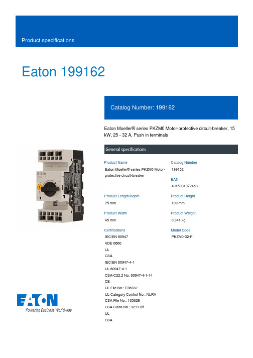
Eaton 199162Eaton Moeller® series PKZM0 Motor-protective circuit-breaker, 15kW, 25 - 32 A, Push in terminalsGeneral specificationsEaton Moeller® series PKZM0 Motor-protective circuit-breaker199162401508197246375 mm109 mm45 mm0.341 kgIEC/EN 60947VDE 0660ULCSAIEC/EN 60947-4-1UL 60947-4-1CSA-C22.2 No. 60947-4-1-14 CEUL File No.: E36332UL Category Control No.: NLRV CSA File No.: 165628CSA Class No.: 3211-05ULCSA PKZM0-32-PIProduct Name Catalog NumberEANProduct Length/Depth Product Height Product Width Product Weight Certifications Model CodeTurn buttonPhase-failure sensitivity (according to IEC/EN 60947-4-1, VDE 0660 Part 102)Motor protectionPhase failure sensitiveThree-pole 100,000 operations100,000 OperationsDIN rail (top hat rail) mounting optionalCan be snapped on to IEC/EN 60715 top-hat rail with 7.5 or15 mm height.40 Operations/hIII3Motor protective circuit breakerFinger and back-of-hand proof, Protection against direct contact when actuated from front (EN 50274)6000 V AC25 g, Mechanical, according to IEC/EN 60068-2-27, Half-sinusoidal shock 10 msAlso motors with efficiency class IE3Branch circuit: Suitable for group installations, (UL/CSA)-5 - 40 °C to IEC/EN 60947, VDE 0660≤ 0.25 %/K, residual error for T > 40°-25 - 55 °C, Operating rangeMotor starter combinations type MSC...Actuator type Features Functions Number of poles Lifespan, electricalLifespan, mechanicalMounting MethodMounting positionOperating frequencyOvervoltage categoryPollution degreeProduct categoryProtectionRated impulse withstand voltage (Uimp) Shock resistanceSuitable forTemperature compensationUsed withMax. 2000 m-25 °C55 °C25 °C40 °C40 °C80 °CDamp heat, cyclic, to IEC 60068-2-30 Damp heat, constant, to IEC 60068-2-781 x (1 - 6) mm²18 - 812 mm50 Hz60 Hz32 A7.5 kW15 kW690 V690 V32 A496 A, Irm, Setting range max. ± 20% tolerance, Trip blocksBasic device fixed 15.5 x Iu, Trip Blocks7.5 HP5 HP10 HP20 HP25 HPAltitude Ambient operating temperature - min Ambient operating temperature - max Ambient operating temperature (enclosed) - min Ambient operating temperature (enclosed) - max Ambient storage temperature - min Ambient storage temperature - max Climatic proofingTerminal capacity (flexible)Terminal capacity (solid/stranded AWG)Stripping length (main cable)Rated frequency - min Rated frequency - max Rated operational current (Ie)Rated operational power at AC-3, 220/230 V, 50 Hz Rated operational power at AC-3, 380/400 V, 50 Hz Rated operational voltage (Ue) - min Rated operational voltage (Ue) - max Rated uninterrupted current (Iu)Short-circuit releaseAssigned motor power at 200/208 V, 60 Hz, 3-phase Assigned motor power at 230/240 V, 60 Hz, 1-phase Assigned motor power at 230/240 V, 60 Hz, 3-phase Assigned motor power at 460/480 V, 60 Hz, 3-phase Assigned motor power at 575/600 V, 60 Hz, 3-phasePush in terminals032 A32 AOverload trigger: tripping class 10 A 9.56 W0 W0 W0 WMeets the product standard's requirements.Meets the product standard's requirements.Meets the product standard's requirements.Meets the product standard's requirements.Meets the product standard's requirements.Does not apply, since the entire switchgear needs to be evaluated.Does not apply, since the entire switchgear needs to be evaluated.Meets the product standard's requirements.Connection Number of auxiliary contacts (change-over contacts)Number of auxiliary contacts (normally closed contacts)Number of auxiliary contacts (normally open contacts)Overload release current setting - min Overload release current setting - max Tripping characteristic Equipment heat dissipation, current-dependent PvidHeat dissipation capacity PdissHeat dissipation per pole, current-dependent PvidStatic heat dissipation, non-current-dependent Pvs10.2.2 Corrosion resistance10.2.3.1 Verification of thermal stability of enclosures10.2.3.2 Verification of resistance of insulating materials to normal heat10.2.3.3 Resist. of insul. mat. to abnormal heat/fire by internal elect. effects10.2.4 Resistance to ultra-violet (UV) radiation10.2.5 Lifting10.2.6 Mechanical impact10.2.7 InscriptionsDoes not apply, since the entire switchgear needs to be evaluated.Meets the product standard's requirements.Does not apply, since the entire switchgear needs to be evaluated.Does not apply, since the entire switchgear needs to be evaluated.Is the panel builder's responsibility.Is the panel builder's responsibility.Is the panel builder's responsibility.Is the panel builder's responsibility.Is the panel builder's responsibility.The panel builder is responsible for the temperature rise calculation. Eaton will provide heat dissipation data for the devices.Is the panel builder's responsibility. The specifications for the switchgear must be observed.Is the panel builder's responsibility. The specifications for the switchgear must be observed.The device meets the requirements, provided the information in the instruction leaflet (IL) is observed.Motor Starters in System xStart - brochureSave time and space thanks to the new link module PKZM0-XDM32MEProduct Range Catalog Switching and protecting motorsSwitching and protecting motors - catalogDA-DC-00004889.pdfDA-DC-00004919.pdf121X042121X002eaton-manual-motor-starters-pkz-dimensions.epseaton-manual-motor-starters-pkz-dimensions-002.epseaton-manual-motor-starters-pkzm-pkzm0-dimensions.epsETN.PKZM0-32-PI.edzIL122024ZUWIN-WIN with push-in technologymotorschutzschalter_bis_32a_pi.dwgpkzm0_pi.stp10.3 Degree of protection of assemblies10.4 Clearances and creepage distances10.5 Protection against electric shock10.6 Incorporation of switching devices and components 10.7 Internal electrical circuits and connections10.8 Connections for external conductors10.9.2 Power-frequency electric strength10.9.3 Impulse withstand voltage10.9.4 Testing of enclosures made of insulating material 10.10 Temperature rise10.11 Short-circuit rating10.12 Electromagnetic compatibility10.13 Mechanical function BrochuresCatalogues Declarations of conformity DrawingseCAD modelInstallation instructions Installation videosmCAD modelEaton Corporation plc Eaton House30 Pembroke Road Dublin 4, Ireland © 2023 Eaton. All rights reserved. Eaton is a registered trademark.All other trademarks areproperty of their respectiveowners./socialmedia。
P4470 Save A Watt Operation Manual

Model P4470Save A Watt ™ Operation ManualThank you for purchasing the P4470 Save A Watt™. This operating manual will provide an overview of the product, safety instructions, a quick guide to operation, and complete instructions for correct usage. Take the time to completely review these instructions as well as safety warnings to ensure your best use of the product.Simply connect your appliances to the Save A Watt ™ -- then you can program ON/OFF periods to save money.The unit combines the advantages of traditional mechanical and electronic timers. It is easy to program on quarter-hour basis ON/OFF periods for 7 days and 24 hours the same as you would program a traditional mechanical timer, and not limited to one day only. On normal electronic timers it is easy to forget which days and which periods are ON or OFF. The P4470 eliminates the need to take notes. You can just press keys to see the detailed 7 day 24 hour ON/OFF setting information. Advanced features also included:● Zero power crossing switch provides a spike free ON/OFF relay control to prolong your appliance usage life. ● LEDs provide a LCD backlight, and a nightlight function.With the innovative Save A Watt ™ you ’ll have peace of mind in more ways than one.Safety Instructions:● The operating voltage is limited to +/- 10% of Line voltage 120Vac. Do not use it in other voltage rating. ● The maximum output current is 15A.● To reduce the risk of electric shock, do not remove cover. No user-serviceable parts inside. Refer servicing to qualified servicepersonnel.Warning:● To reduce the risk of fire or electric shock, do not expose this appliance to rain or moisture.Feature Locations:OutletLCD DisplayWith Backlight orange LED Auto Key with orange LED OFF Key with red LED ON Key with green LEDSoft function keyDisplay Panel:LCD DisplayWith Backlight (Orange LED)Soft function keyWeekly Day IconProgram Setting IndicatorLow Battery Icon Function IndicatorAM/PM Icon Back Light IconMain DisplayHigh Temp. IconHoliday IconQuick Start Guide:Use these quick start instructions to get up and running in just a few minutes. Be sure to review all the operating instructions later to ensure full enjoyment of the product.1. Using the appropriate flat screwdriver open the battery holder, and insert 3 (AAA/no. 4) batteries, according to the +/- terminal.When the batteries are in place, press the battery holder back into its original position. Now you can operate the unit by battery power allowing you to program the unit without plugging it into a wall outlet. 2. Connect the Save A Watt ™ unit to the outlet and the appliance to the unit.3. Clock mode is the initial mode, the main display will be a flashing clock, please refer to clock mode to set clock time later.4.Press the OFF key. The OFF key will illuminate red.5. Press the ON key. The ON key will illuminate green and the attached appliance will be powered. Turn on the appliance.6. Press the Program Function key, one segment of outer LCD will flash, and main display will show Mon. Pressing the Day key willcycle through Mon, Tue, Wed, Thu, Fri, Sat, Sun and Back Light.7. Press the Delay Off Function key, Delay Off initial value is 30 minute and will show on main display. 8. Press the Clock Function key, the main display will show the flashing clock. 9. Press the Return key to function key menu.10. Any key press, will illuminate the orange backlight for around 5 seconds. 11. Review the complete operating instructions to familiarize yourself with all features.Installation:1. Using the appropriate flat screwdriver open the battery holder, and insert 3 (AAA/no. 4) batteries, according to the +/- terminal.When the batteries are in place, press the battery holder back into its original position. Now you can operate the unit by battery power allowing you to program the unit without plugging it into a wall outlet.2. Turn off the appliance before connection to the unit and remove the power cord from the outlet. Connect the Save A Watt ™ unit tothe outlet and appliance to the unit.3. The main display of LCD will be flashing in Clock mode. This is normal when the unit is first connected to power, please refer toClock mode to set the clock time.4. Press the ON key, and Turn the appliance back on and confirm normal operation. If the appliance does not function, pleaserecheck your installation.ON, OFF and Auto key function:1. Pressing the OFF key will turn off power to outlet at once. The OFF key will illuminate in red, and the function keys and LCDdisplay will continue to operate.2. Pressing the ON key will turn power on to outlet at once. The ON key will illuminate in green. The unit features a spike-free switchfunction which activates at zero-crossing and will present clean power to your connected appliance, and the function keys and LCD display will operate.3. Pressing the Auto key to Auto mode, the Auto key will illuminate in orange. It will activate the unit automatically ON or OFFaccording to the Program. If the Program is ON, the unit will be ON at once no matter the previous status. If the Program is OFF, the unit will be OFF at once no matter the previous status. Pressing the Auto key again to Manual mode can disable auto ON or OFF function and the Auto key LED will be dark. The unitwill always switch ON or OFF according to the latest ON or OFF status until you press the ON or OFF or Auto key.Clock mode:(Clock Function key → Day key, Hour key, or Minute key can adjust Clock → Return key).1. Press the Clock Function key to Clock mode, the main display will be the flashing clock, and Mon is displayed. This is normalwhen the unit is first connected to power, it will always flash until the current time is set.2. Pressing Day key - main display will flash and pressing Day key again will cycle through Mon, Tue, Wed, Thu, Fri, Sat and Sun.3. Pressing Hour key - main display will flash and pressing Hour key again will increase in one hour steps.4. Pressing Min key - main display will flash and pressing Min key again will increase in one minute steps.5. Press the Return key to return back to the function key menu.Program mode:(Program Function key → Day key, on/I key, or off/0 key can program Timer ON/OFF in 7 days 24 hours → Return key).(Program Function key → Day key to no weekly day display →on/ I key, off/0 key can program Back Light → Return key).1. Press the Program Function key to Program mode - main display shows current time, the current time corresponding cursor ofthe outer LCD will be flashing, the segment is a quarter-hour (15 minute) period.2. Pressing the Day key will cycle through Mon, Tue, Wed, Thu, Fri, Sat,Sun and Back Light. Please select the correct day.3. Pressing the on/I key, the current flashing cursor of outer LCD will be set to on and flashing cursor will be moved to the nextsegment for setting.4. Pressing off/0 key, the current flashing cursor of outer LCD will be set to off and flashing cursor will be moved to the next segmentfor setting.5. Press the Return key to back to function key menu.6. In Back Light mode, the orange back light will be turned on or off according to program setting automatically, independent of theunit ON or OFF condition.7. The Auto key has no function under Program mode.Example: Monday AM 06:00 to AM 08:00 is ON,PM 07:00 to PM 10:00 is ON,Other time period is OFF.Program function key → Day key to Mon → off/0 key until main display to AM 06:00 → on/I key until main display to AM 08:00 → off/0 key until main display to PM 07:00 → on/I key until main display to PM 10:00 → Return key.12AMMondayNow is AM 10:10Corresponding Cursor(1/8 duty flash)Example: Saturday AM 08:00 to AM 10:00 is ON,PM12:00 to PM 01:00 is ON,PM 06:00 to PM 11:00 IS ON,Other time period is OFF.Program function key → Day key to Sat → off/0 key until main display to AM 08:00 → on/I key until main display to AM 10:00 → off/0 key until main display to PM 12:00 → on/I key until main display to PM 01:00 → off/0 key until main display to PM 06:00 → on/I key until main display to PM 11:00 → Return key.12AMSaturdayNow is PM 5:40Corresponding Cursor(1/8 duty flash)Example: Back Light for every PM 06:00 to AM 06:00.Program function key → Day key until no Mon to Sun icon show up → on/I key until AM 06:00 → off/0 key until PM 06:00 → on/I key until AM 00:00 → Return key.12AMCorresponding CursorSetting TimeUnderstanding the Auto Copy function:For initial programming (first time to program) or holding the first key (Program or Day key) and the fourth key (Return key) simultaneously for around 3 seconds – the unit will reset all segments to be off. Now you can program Monday and by pressing the Day key to function key menu you will get the Auto Copy function, Monday’s program will automatically copy to the other days, Tue to Sun. Now all 7 days programming is identical and it is easy for you to make slight modifications to adapt 7 days schedule to your preference.Understand the Holiday mode:Press the Holiday function key to activate the Holiday mode - the main display shows the current time, the current time corresponding cursor of the outer LCD will be flashing, but the Timer on/off program function follows the programming for Sunday. This is a great advantage for you to use the Timer when you are on a holiday, but it is not on Sunday. Pressing the Holiday function key again will return to the original status.Example: Monday AM 06:00 to AM 08:00 is ON.PM 07:00 to PM 11:00 is ON.Other time period is OFF.Sunday PM 01:00 to PM 06:00 is OFF.Other time period is ON.MondayAM 06:00~AM 08:00 ON PM 07:00~PM 11:00 ONThe other is OFFSundayPM 01:00~PM 06:00 OFFThe other is ON12 AMMondayAM 06:00~AM 08:00 ON PM 07:00~PM 10:00 ONThe other is OFFHolidayPM 01:00~PM 06:00 OFFThe other is ONCursorNow is AM 10:10Now is Monday 12 AM12 AMDelay OFF mode: (Delay OFF function key → Hour key, Minute key can set count down period → Return key).1. Press the Delay OFF function key to select the Delay OFF mode. The main display will show the latest set count down time or 30minutes (factory default), the colon between hour and minute will be flashing to start the count down. The unit will be in the ON mode now. After the count down time reaches zero, the unit will switch to the OFF mode. 2. Pressing the Hour key will increment the hour setting by one, and cycle through 0 to 23. 3. Pressing the Minute key will increment the minute setting by one and cycle through 0 to 59. 4. Pressing the Return key returns back to the function key menu.5. Pressing OFF key will stop the count down time. For example, the start time is 30 minutes, when there are 17 minutes left, thenpress the OFF key. The unit will stay at 17 minute left. When you press the ON key, the unit will re-start to count down from the original time (default 30 minutes).6. The Auto key has no function under Delay OFF mode.Example: Countdown 30 minutes.Delay OFF Function key → Return →ON key (if OFF condition).Countdown12 AMBattery back up function:1. When power to the unit is interrupted, the internal power supply will be switched to battery back up mode immediately. The LEDbacklight is disabled if AC power is interrupted.2. This allows the user to take unit anywhere to set and enter programming. It is more convenient for the user to set and enterprogramming the unit when not plugged into the wall.3. When the unit is plugged back in or AC line power is restored, the internal power supply will be switched back to AC line power.The batter will be conserved for future use.4. To replace Battery- using the appropriate flat screwdriver open the battery holder, and position the 3 (AAA/no. 4) batteries,according to the +/- terminal. When the batteries are in place, press the battery holder back into its original position.Retained Program:1. User programmed Timer ON/OFF and Delay OFF settings are retained in EEPROM after every update, to prevent the loss ofsettings when power is interrupted or when the backup batteries are exhausted.Over temperature protection function:In an over current condition or if the plug and socket contact is not strong, the plug and socket contact temperature may increase. Under this condition, the power will be switched off to the outlet. The OFF key will illuminate in red. The main display High Temp. Icon will flash, and the audible alarm will sound. Remove the appliance, press the OFF key to turn off the audible alarm and erase the main display High Temp. icon. Then press ON key to turn the power back on.12 AM Specification:Trouble Shooting:Maintenance●Protect the Timer from adverse weather conditions. The Timer is not waterproof. Do not expose the LCD display to directsunlight for long periods of time.●CAUTION: To avoid damage to the Timer, do not expose it to sprays, liquids, or solvents.●Clean the exterior of the Timer by removing dust with a lint-free cloth.●Use care to avoid scratching the clear plastic display filter.●For further cleaning, use a soft cloth or paper towel dampened with water. You can use a 75% isopropyl alcohol solution for moreefficient cleaning.●CAUTION: To avoid damage to the surface of the Timer, do not use abrasive or chemical cleaning agents.P3 INTERNATIONAL CORPORATIONLIMITED WARRANTYP3 INTERNATIONAL CORPORATION ("P3") warrants to the original retail purchaser only, that its product is free from defects in material or workmanship under the condition of normal use and service for a period of six (6) months from the date of purchase. In the event that a defect, malfunction or failure occurs or is discovered during the warranty period, P3 will repair or replace at its option the product or component part(s) which shall appear in the reasonable judgment of P3 to be defective or not to factory specifications.A product requiring service is to be returned to P3 along with the sales receipt or other proof of purchase acceptable to P3 and astatement describing the defect or malfunction. All transportation costs shall be borne by the owner and the risk of loss shall be upon the party initiating the transportation. All items repaired or replaced thereunder shall be subjected to the same limited warranty for a period of six (6) months from the day P3 ships the repaired or replaced product. The warranty does not apply to any product that has been subject to misuse, tampering, neglect, or accident or as a result of unauthorized alterations or repairs to the product. This warranty is void if the serial number (if any) has been removed, altered, or defaced. This warranty is in lieu of all warranties expressed or implied, including the implied warranties of merchantability and fitness for a particular purpose which are expressly excluded or disclaimed. P3 shall not be responsible for consequential, incidental or other damages, and P3 expressly excludes and disclaims liability for any damages resulting from the use, operation, improper application, malfunction or defeat of any P3 product covered by this limited warranty. P3's obligation is strictly and exclusively limited to the replacement or repair of any defective product or component part(s). Some states do not allow the exclusion or limitation of incidental or consequential damages, so the above limitation or exclusion may not apply to you. P3 does not assume or authorize anyone to assume for it any other obligation whatsoever. Some states do not allow limitation on how long an implied warranty lasts, so the above limitations may not apply to you.It is the owner/user's responsibility to comply with local, state, or federal regulations, if any, that may pertain to P3 products or their use.This warranty gives you specific legal rights, and you may also have other rights which vary from state to state.If you experience difficulty in the operation of your unit, or if your unit requires repair please contact:P3 INTERNATIONAL CORPORATIONTECHNICAL SUPPORTTel: 212-741-7289Fax: 212-741-2288Email: *******************************REV. 0110。
和谐XPS安全自动化产品数据表说明书

Product data sheetSpecificationsTime delayed output, Harmony XPS,for Estop, guard, OSSD, 24 V AC/DC, springXPSBAT12A1ACMainRange of ProductHarmony Safety Automation Product or Component Type Safety module Safety module name XPSBATSafety module application For emergency stop and protective guard applications For OSSD monitoringFunction of moduleEmergency stop button with 2 NC contacts Guard monitoring with 1 or 2 limit switches Light curtain monitoring RFID switchMonitoring of electro-sensitive protection equipment (ESPE)Safety levelCan reach PL e/category 4 for normally open relay contact ISO 13849-1Can reach SILCL 3 for normally open relay contact IEC 62061Can reach SIL 3 for normally open relay contact IEC 61508Can reach PL c/category 1 for normally closed relay contact ISO 13849-1Can reach SILCL 1 for normally closed relay contact IEC 62061Can reach SIL 1 for normally closed relay contact IEC 61508Safety reliability dataMTTFd > 30 years ISO 13849-1Dcavg >= 99 % ISO 13849-1PFHd = 0.98E-09 for SS0 ISO 13849-1PFHd = 0.96E-09 for SS1 ISO 13849-1HFT = 1 IEC 62061PFHd = 0.98E-09 for SS0 IEC 62061PFHd = 0.96E-09 for SS1 IEC 62061SFF > 99% IEC 62061HFT = 1 IEC 61508-1PFHd = 0.98E-09 for SS0 IEC 61508-1PFHd = 0.96E-09 for SS1 IEC 61508-1SFF > 99% IEC 61508-1Type = B IEC 61508-1Electrical circuit type NC pair OSSD pairConnections - terminalsRemovable spring terminal block, 0.2...2.5 mm² solid or flexibleRemovable spring terminal block, 0.25...2.5 mm² flexible with ferrule single conductor Removable spring terminal block, 0.2...1.5 mm² solid or flexible twin conductorRemovable spring terminal block, 2 x 0.25...1 mm² flexible with ferrule without cable end, with bezel Removable spring terminal block, 2 x 0.5...1.5 mm² flexible with ferrule with cable end, with bezel [Us] Rated Supply Voltage24 V AC - 15...10 %24 V DC - 20...20 %ComplementarySynchronisation time between inputs 0.5 s 2 sType of startAutomatic/manual/monitored Power consumption in W2 W 24 V DCD i s c l a i m e r : T h i s d o c u m e n t a t i o n i s n o t i n t e n d e d a s a s u b s t i t u t e f o r a n d i s n o t t o b e u s e d f o r d e t e r m i n i n g s u i t a b i l i t y o r r e l i a b i l i t y o f t h e s e p r o d u c t s f o r s p e c i f i c u s e r a p p l i c a t i o n sPower consumption in VA5 VA 24 V AC 50/60 HzInput protection type Internal, electronicSafety outputs 2 NO1 NOSafety inputs2Maximum wire resistance500 OhmTime delay range0...900 sInput compatibility Normally closed circuit ISO 14119Mechanical contact ISO 14119OSSD pair IEC 61496-1-2Normally closed circuit ISO 138503-wire proximity sensors PNP[Ie] rated operational current5 A AC-13 A AC-155 A DC-13 A DC-13Control outputs 3 pulsed outputInput/Output type Semiconductor output Z1, 20 mA[Ith] conventional free air12 Athermal currentAssociated fuse rating6 A gG NO relay output circuit IEC 60947-1 Minimum output current20 mA relay outputMinimum output voltage24 V relay outputMaximum response time on20 msinput open[Ui] rated insulation voltage250 V 2)EN/IEC 60947-1[Uimp] rated impulse withstand4 kV II EN/IEC 60947-1voltageLocal signalling LED green power power ONLED red error errorLED yellow state 1 safety output instantaneousLED yellow state 2 safety output delayedLED yellow start 1 startLED yellow start 2 startLED yellow S12 safety input S12LED yellow S22 safety input S22Mounting Support35 mm symmetrical DIN railDepth 4.72 in (120 mm)Height 3.94 in (100 mm)Width 1.77 in (45 mm)Net Weight0.77 lb(US) (0.350 kg)EnvironmentStandards IEC 60947-5-1IEC 61508-1 functional safety standardIEC 61508-2 functional safety standardIEC 61508-3 functional safety standardIEC 61508-4 functional safety standardIEC 61508-5 functional safety standardIEC 61508-6 functional safety standardIEC 61508-7 functional safety standardISO 13849-1 functional safety standardIEC 62061 functional safety standardProduct certifications TÜVcULusIP degree of protection IP20 terminals)EN/IEC 60529IP40 housing)EN/IEC 60529IP54 mounting area)EN/IEC 60529 Ambient air temperature for-13…131 °F (-25…55 °C)operationAmbient Air Temperature for-13…185 °F (-25…85 °C)StorageRelative Humidity5…95 % non-condensingOrdering and shipping detailsCategory22477-SAFETY MODULES (PREVENTA)Discount Schedule SAF2GTIN3606482034037Nbr. of units in pkg.1Package weight(Lbs)10.65 oz (302 g)Returnability NoPacking UnitsUnit Type of Package 1PCEPackage 1 Height 2.52 in (6.4 cm)Package 1 width 5.24 in (13.3 cm)Package 1 Length 6.02 in (15.3 cm)Unit Type of Package 2S03Number of Units in Package 216Package 2 Weight11.92 lb(US) (5.409 kg)Package 2 Height11.81 in (30 cm)Package 2 width11.81 in (30 cm)Package 2 Length15.75 in (40 cm)Package 3 Height11.81 in (30 cm)Offer SustainabilitySustainable offer status Green Premium productCalifornia proposition 65WARNING: This product can expose you to chemicals including: Lead and lead compounds, which isknown to the State of California to cause cancer and birth defects or other reproductive harm. For moreinformation go to REACh Regulation REACh DeclarationEU RoHS Directive Pro-active compliance (Product out of EU RoHS legal scope)EU RoHS DeclarationMercury free YesRoHS exemption information YesChina RoHS Regulation China RoHS declarationEnvironmental Disclosure Product Environmental ProfileCircularity Profile End of Life InformationWEEE The product must be disposed on European Union markets following specific waste collection andnever end up in rubbish bins.Dimensions Drawings DimensionsFront and Side Views(A) : Product drawing(B) : Spring terminal(C) : Side view(1) : Removable terminal blocks, top(2) : Removable terminal blocks, bottom(3) : LED indicators(4) : Delay factor selector(5) : Delay base selector(6) : Sealable transparent coverMounting to DIN railScrew-mountingConnections and SchemaWiring Diagram(1) : A1-A2 (Power supply)(2) : S11–S21 (Control outputs (DC+) of safety-related inputs), S12-S22 (Input channels (CH+) of safety-related inputs)(3) : Y1 (Control output of Start/Restart input), Y2 (Input channel for automatic/manual start), Y3 (Input channel for monitored start with falling edge)13-14-23-24 : Terminals of the safety-related outputs (instantaneous)37-38 : Terminals of the safety-related outputs (delayed)Z1 : Solid state output, not safety-related。
35670a dynamic signal analyzer datasheet说明书
Keysight Technologies35670A Dynamic Signal AnalyzerVersatile two- or four-channel high-per f or m anceFFT-based spectrum/network an a l yz e r122 µHz to 102.4 kHz 16-bit ADCData SheetSummary of Features on Standard InstrumentThe following features are standard with the Keysight Technologies, Inc. 35670A:Instrument modesFFT analysis Histogram/time Correlation analysis Time captureMeasurementFrequency domainFrequency response Power spectrumLinear spectrum CoherenceCross spectrum Power spectral density Time domain (oscilloscope mode)Time waveform AutocorrelationCross-correlation Orbit diagram Amplitude domainHistogram, PDF, CDFTrace coordinatesLinear magnitude Unwrapped phaseLog magnitude Real partdB magnitude Imaginary partGroup delay Nyquist diagramPhase PolarTrace unitsY-axis amplitude: combinations of units, unit value, calculated value, and unit format describe y-axis amplitude Units: volts, g, meters/sec2, inches/sec2, meters/sec, inches/sec, meters, mils, inches, pascals, Kg, N, dyn, lb, user-defined EUsUnit value: rms, peak, peak-to-peakCalculated value: V, V2, V2/Hz, √Hz, V2s/Hz (ESD)Unit format: linear, dB’s with user selectable dB reference, dBm with user selectable impedance.Y-axis phase: degrees, radiansX-axis: Hz, cpm, order, seconds, user-defined Display formatsSingleQuadDual upper/lower tracesSmall upper and largelowerFront/back overlay traces Measurement stateBode diagramWaterfall display with skew, -45 to 45 degrees Trace grids on/offDisplay blankingScreen saverDisplay scalingAutoscale Selectable reference Manual Scale Linear or log X-axis Input range tracking Y-axis logX & Y scale markers with expand and scrollMarker functionsIndividual trace markersCoupled multi-trace markersAbsolute or relative markerPeak searchHarmonic markersBand markerSideband power markersWaterfall markersTime parameter markersFrequency response markersSignal averaging (FFT mode) Average types (1 to 9,999,999 averages) RMS Time exponential RMS exponential Peak holdTimeKey SpecificationsFrequency range102.4 kHz 1 channel51.2 kHz 2 channel25.6 kHz 4 channelDynamic range90 dB typicalAccuracy ±0.15 dBChannel match±0.04 dB and ±0.5 degreesReal-time bandwidth25.6 kHz/1 channelResolution100, 200, 400, 800 & 1600 linesTime capture> 6 MsamplesSource types Random, burst random, periodic chirp, burst chirp, pink noise,sine, swept-sine (Option 1D2), arbitrary (Option 1D4)Math+,-,*, / Conjugate Magnitude Real and imaginary Square Root FFT, FFT -1LN EXP *jω or /jω PSD Differentiation A, B, and C weighting Integration Constants K1 thru K5 Functions F1 thru F5AnalysisLimit test with pass/failData table with tabular readout Data editingTime capture functionsCapture transient events for repeated analysis in FFT, octave, order, histogram, or correlation modes (except swept-sine). Time-captured data may be saved to internal or external disk, or transferred over GPIB. Zoom on captured data for detailed nar r ow b and analysis.Data storage functionsBuilt-in 3.5 in., 1.44-Mbyte flexible disk also supports 720-KByte disks, and 2 Mbyte NVRAM disk. Both MS-DOS and HP-LIF formats are available. Data can be formatted as either ASCII or binary (SDF). The 35670A provides storage and recall from the internal disk, internal RAM disk, internal NVRAM disk, or external GPIB disk for any of the following information:Instrument setup states Trace data User-mathLimit dataTime capture buffers Keysight Instrument BASIC Waterfall display data ProgramsData tablesCurve fit/synthesis tablesGPIB capabilitiesConforms to IEEE 488.1 /488.2Conforms to SCPI 1992Controller with Keysight Instrument Basic OptionCalibration & memorySingle or automatic calibration Built-in diagnostics & service tests Nonvolatile clock with time/dateTime/date stamp on plots and saved data filesOnline help Access to topics via keyboard or index FanOn/OffAveraging controlsOverload rejectFast averaging on/off Update rate selectSelect overlap process percentage Preview time recordMeasurement controlStart measurementPause/continue measurementTriggeringContinuous (Freerun)External (analog or TTL level)Internal trigger from any channel Source synchronized trigger GPIB trigger Armed triggers Automatic/manual RPM step Time stepPre- and post-trigger measurement DelayTachometer input±4 V or ±20 V range40 mv or 200 mV resolution Up to 2048 pulses/rev Tach hold-off controlSource outputsRandom Burst random Periodic chirp Burst chirp Pink noise Fixed sineNote: Some source types are not available for use in optional modes. See option description for details.Input channelsManual range Anti-alias filters On/Off Up-only auto range AC or DC coupling Up/down auto range LED half range and overload indicators Floating or grounded A-weight filters On/Off Transducer power supplies (4 ma constant current)Frequency20 spans from 195 mHz to 102.4 kHz (1 channel mode)20 spans from 98 mHz to 51.2 kHz (2 channel mode)Digital zoom with 244 µHz resolution throughout the 102.4 kHz frequency bands.Resolution 100, 200, 400, 800 and 1600 linesWindowsHann UniformKeysight 35670A SpecificationsInstrument specifications apply after 15 minutes warm-up and within 2 hours of the last self-calibration. When the internal cooling fan has been turned OFF, specifications apply within 5 minutes of the last self-cal i b ra t ion. All speci-fications are with 400 line frequency resolution and with anti-alias filters enabled unless stated otherwise.FrequencyMaximum range**1 channel mode102.4 kHz,51.2 kHz (opt AY6*)2 channel mode51.2 kHz4 channel mode (Option AY6 only) 25.6 kHzSpans1 channel mode195.3 mHz to 102.4 kHz2 channel mode97.7 mHz to 51.2 kHz 4 channel mode (Option AY6 only) 97.7 mHz to 25.6 kHz Minimimum resolution1 channel mode122 µHz (1600 linedisplay)2 channel mode61 µHz (1600 linedisplay)4 channel mode (Option AY6 only)122 µHz (800 linedisplay) Maximum real-time bandwidthFFT span for continuous data acquistion)(Preset, fast averaging)1 channel mode25.6 kHz2 channel mode12.8 kHz4 channel mode (Option AY6 only) 6.4 kHz Measurement rate(Typical) (Preset, fast averaging)1 channel mode≥ 70 averages/sec2 channel mode≥ 33 averages/sec4 channel mode (Option AY6 only)≥ 15 averages/sec Display update rateTypical (Preset, fast average off)≥ 5 updates/Sec Maximum ≥ 9 updates/Sec (Preset, fast average off, single channel, single display, undisplayed trace displays set to data registers)Accuracy±30 ppm (.003%)Single channel ampltudeAbsolute amplitude accuracy (FFT)(A combination of full scale accuracy, full scale flatness, and amplitude linearity.)±2.92% (0.25 dB) of reading±0.025% of full scaleFFT full scale accuracy at 1 kHz (0 dBfs)±0.15 dB (1.74%)FFT full scale flatness (0 dBfs) relative to 1 kHz±0.2 dB (2.33%)FFT amplitude linearity at 1 kHz measured on +27 dBVrms range with time avg, 0 to -80 dBfs±0.58% (0.05 dB) of reading±0.025% of full scaleAmplitude resolution(16 bits less 2 dB over-range) with averaging 0.0019% of full scale (typical)Residual DC response (FFT mode)Frequency display (excludes A-weight filter)<-30 dBfs or 0.5 mVdcFFT dynamic rangeSpurious free dynamic range(Includes spurs, harmonic distortion, intermodulation distortion, alias products). Excludes alias responses at extremes of span. Source impedence = 50 Ω.800 line display.90 dB typical (<-80 dBfs)* O ption AY6 single channel maximum range extends to 102.4 kHz without anti-alias filter protection.** S how all lines mode allows display of up to 131.1, 65.5 and 32.7 kHz respectively. Amplitudes accuracy is unspecified and not alias protected.Full span FFT noise floor (typical)Flat top window, 64 RMS averages, 800 line display.Harmonic distortion<-80 dBfs Single Tone (in band), ≤ 0 dBfs Intermodulation distortion<-80 dBfs Two tones (in-band), each ≤ -6.02 dBfs Spurious and residual responses <-80 dBfsSource impedence = 50 Ω.Frequency alias responsesSingle tone (out of displayed range), ≤ 0 dBfs, ≤ 1 MHz(≤ 200 kHz with IEPE transducer power supply On)2.5% to 97.5% of the frequency span <-80 dBfs Lower and upper 2.5% of frequency span<-65 dBfsInput noiseInput noise levelFlat top window, -51 dBVrms range Source impedance = 50 ΩAbove 1280 Hz <-140 dBVrms/√2Hz 160 Hz to 1280 Hz <-130 dBVrms/√2Hz Note: To calculate noise as dB below full scale:Noise [dBfs] = Noise [dB/√2Hz] + 10LOG(NBW) - Range [dBVrms]; where NBW is the noise equivalent BW of the window (see below).Window parametersUniformHannFlat top-3 dB bandwidth*0.125% of span 0.185% of span 0.450% of span Noise equivalent bandwidth*0.125% of span 0.1875% of span 0.4775% of span Attenuation at ±1/2 bin 4.0 dB 1.5 dB 0.01 dB Shape factor(-60 dB BW/-3 dB BW)7169.1 2.6* For 800 line displays. With 1600, 400, 200, or 100 line displays, multiply bandwidths by 0.5, 2, 4, and 8, respectively.dB below full scaleTypical noise floor vs. range for different frequency spans-51 -41 -31 -21 -11 27 0.0028 0.0089 0.028 0.089 0.28022.4-100 dB/0.001%Amplitude range (dBVrms / Vrms)-90 dB/0.003%-80 dB/0.01% -70 dB/0.03%51.2 kHz Span 6.4 kHz Span 800 Hz SpanSingle channel phasePhase accuracy relative to externaltrigger± 4.0 deg16 time averages center of bin,DC coupled 0 dBfs to -50 dBfs only0 Hz < freq ≤ 10.24 kHz onlyFor Hann and flat top windows, phase is relative to a cosine wave at the center of the time record. For the uniform, force, and exponential windows, phase is relative to a cosine wave at the beginning of the time record.Cross-channel amplitudeFFT cross-channel gain accuracy± 0.04 dB (0.46%) Frequency response modeSame amplitude rangeAt full scale: Tested with 10 RMSaverages on the -11 to +27 dBVrmsranges, and 100 RMS averages onthe -51 dBVrms rangeCross-channel phaseCross-channel phase accuracy(Same conditions as cross-channelamplitude)± 0.5 degInputInput ranges (full scale)(Auto-range capability)+27 dBVrms (31.7 Vpk) to -51 dBVrms(3.99 mVpk) in 2 dB steps Maximum input levels42 VpkInput impedance 1 MΩ ±10%90 µF nominalLow side to chassis impedance Floating modeGrounded mode 1 MΩ ±30% (typical) <0.010 µF≤100 ΩAC coupling rolloffSource impedance = 50 Ω<3 dB rolloff at 1 HzCommon mode rejection ratioSingle tone at or below 1 kHz-51 dBVrms to -11 dBVrms ranges>75 dB typical-9 dBVrms to +9 dBVrms ranges>60 dB typical+11 dBVrms to +27 dBVrms ranges>50 dB typical and unfiltered time displayDC amplitude accuracy ±5.0 %fs Rise time of -1 V to 0 V test pulse<11.4 µSec Settling time of -1 V to 0 V test pulse<16 µSec to 1% Peak overshoot of -1 V to 0 Vtest pulse<3% Sampling period1 channel mode 3.815 µSec to2 Sec in 2x steps2 channel mode 7.629 µSec to 4 Sec in 2x steps4 channel mode 15.26 µSec to 8 Sec in 2x steps (Option AY6 only)Pulses per RevolutionRPM 5 ≤ RPM ≤ 491,519 RPM Accuracy±100 ppm (0.01%)(typical)Tach level range Low range High range -4 V to +4 V -20 V to +20 VTach level resolution Low rangeHigh range 39 mV 197 mVMaximum tach input level ±42 Vpk Minimum tach pulse width600 nSec Maximum tach pulse rate400 kHz (typical)PC-style 101-keykeyboardGPIBConforms to the following standards:IEEE 488.1 (SH1, AH1, T6, TE0, L4, LE0, SR1, RL1, PP0,DC1, DT1, C1, C2, C3, C12, E2)EEE 488.2-1987Complies with SCPI 1992Data transfer rate (REAL 64 Format)< 45 mSec for a 401 point traceSerial port Parallel port External VGA portComputed order tracking – Option 1D0 Maximum order x Maximum RPM(—————————————— )≤ 60Online (real time)1 channel mode 25,600 Hz2 channel mode 12,800 Hz 4 channel mode 6,400 HzCapture playback 1 channel mode 102,400 Hz2 channel mode 51,200 Hz 4 channel mode 25,600 HzNumber of orders ≤ 200 5 ≤ RPM ≤ 491,519(Maximum useable RPM is limited by resolution, tach pulse rate,pulses/revolution and average mode settings.)Delta order 1/128 to 1/1Resolution ≤ 400(Maximum order)/(Delta order)Maximum RPM ramp rate 1000 RPM/second real-time(typical)1000 - 10,000 RPM run up Maximum order 10Delta order 0.1RPM step 30 (1 channel)60 (2 channel)120 (4 channel)Order track amplitude accuracy±1 dB (typical)Real time octave analysis – Option 1D1StandardsConforms to ANSI Standard S1.11 - 1986, Order 3, Type 1-D, extended and optional frequency rangesConforms to IEC 651-1979 Type 0 Impulse, and ANSI S1.41 second stable average Single tone at band center:≤ ± 0.20 dBReadings are taken from the linear total power spectrum bin. It is derived from sum of each filter.1/3-octave dynamic range > 80 dB (typical) per ANSI S1.11-1986Frequency ranges (at centers)Online (real time):Single channel 2 channel4 channel1/1 octave 0.063 - 16 kHz 0.063 - 8 kHz 0.063 - 4 kHz 1/3 octave 0.08 - 40 kHz 0.08 - 20 kHz 0.08 - 10 kHz 1/12 octave0.0997 - 12.338 kHz 0.0997 - 6.169 kHz 0.0997 - 3.084 kHz Capture playback1/1 octave 0.063 - 16 kHz 0.063 - 16 kHz 0.063 - 16 kHz 1/3 octave 0.08 - 31.5 kHz 0.08 - 31.5 kHz 0.08 - 31.5 kHz 1/12 octave0.0997 - 49.35 kHz0.0997 - 49.35 kHz0.0997 - 49.35 kHzOne to 12 octaves can be measured and displayed.1/1-, 1/3-, and 1/12-octave true center fre q uen c ies related by the formula: f(i+1)/f(i) = 2^(1/n); n=1, 3, or 12; where 1000 Hz is the reference for 1/1, 1/3 octave, and 1000*2^(1/24) Hz is the reference for 1/12 octave. The marker returns the ANSI standard preferred frequencies.Swept sine measurements – Option 1D2Dynamic range130 dBTested with 11 dBVrms source level at: 100 mSec integration Curve fit/synthesis – Option 1D320 Poles/20 zeroes curve filter frequency response synthesis pole/zero, pole residue & polynomical format Arbitrary waveform source – Option 1D4Amplitude rangeAC: ±5 V peak*DC: ±10 V** Vac pk + |Vdc| ≤ 10 VRecord length # of points = 2.56 x lines ofresolution, or # of complex points = 1.28 x lines of resolution DAC resolution0.2828 Vpk to 5 Vpk 0 Vpk to 0.2828 Vpk2.5 mV 0.25 mVGeneral specificationsSafety standards CSA certified for electronictest and measurementequipment per CSA C22.2, NO.231 This product is designedfor compliance to: UL1244,Fourth Edition IEC 348, 2ndEdition, 1978EMI / RFI standards CISPR 11Acoustic power LpA < 55 dB (Cooling fan athigh speed setting)< 45 dB (Auto speed settingat 25 °C)Fan speed settings of high, automatic, and off are available. The fan off setting can be enabled for a short period of time, except at higher ambient temperatures where the fan will stay on. Environmental operating restrictionsOperating: Disk in drive Operating:No disk in driveStorage &transportAmbient temp. 4 °C to 45 °C0 °C to 55 °C-40 °C to 70 °C Relative humidity(non-condensing)Minimum20%15%5%Maximum80% at 32 °C95% at 40 °C95% at 50 °C Vibrations (5 - 500 Hz)0.6 Grms 1.5 Grms 3.41 Grms Shock 5 G (10 mSec 1/2 sine) 5 G (10 mSec 1/2 sine)40 G (3 mSec 1/2 sine)Max. altitude4600 meters(15,000 ft.)4600 meters(15,000 ft.)4600 meters(15,000 ft.)AC power90 Vrms - 264 Vrms(47 - 440 Hz)350 VA maximumDC power12 VDC to 28 VDC nominal200 VA maximumDC current at 12 V Standard: <10 A typical4 channel: <12 A typical Warm-up time15 minutesWeight15 kg (33 lb) net29 kg (64 lb) shippingD imensions (Excluding bail handle and impact cover) Height190 mm (7.5")Width340 mm (13.4")Depth465 mm (18.3")AbbreviationsdBVrms dB relative to 1 Volt rms.dBfs dB relative to full scale amplitude range.Full scale is approx. 2 dB below ADC overload. Typical Typical, non-warranted, performance specification included to provide general product information.General SpecificationsThis information is subject to change without notice.© Keysight Technologies, 2009 - 2017Published in USA, December 1, 20175966-3064E10 | Keysight | 35670A Dynamic Signal Analyzer - Data Sheet/find/35670AmyKeysight/find/mykeysightA personalized view into the information most relevant to you. /find/emt_product_registrationRegister your products to get up-to-date product information and find warranty information.Keysight Services/find/serviceKeysight Services can help from acquisition to renewal across your instrument’s lifecycle. Our comprehensive service offerings—one-stop calibration, repair, asset management, technology refresh, consulting, training and more—helps you improve product qualityand lower costs.Keysight Assurance Plans/find/AssurancePlansUp to ten years of protection and no budgetary surprises to ensure your instruments are operating to specification, so you can rely on accurate measurements.Keysight Channel Partners/find/channelpartnersGet the best of both worlds: Keysight’s measurement expertise and product breadth, combined with channel partner convenience.For more information on KeysightTechnologies’ products, applications or services, please contact your local Keysight office. The complete list is available at:/find/contactus Americas Canada (877) 894 4414Brazil 55 11 3351 7010Mexico001 800 254 2440United States (800) 829 4444Asia Pacific Australia 1 800 629 485China800 810 0189Hong Kong 800 938 693India 1 800 11 2626Japan 0120 (421) 345Korea 080 769 0800Malaysia 1 800 888 848Singapore 180****8100Taiwan0800 047 866Other AP Countries (65) 6375 8100Europe & Middle East Austria 0800 001122Belgium 0800 58580Finland 0800 523252France 0805 980333Germany ***********Ireland 1800 832700Israel 1 809 343051Italy800 599100Luxembourg +32 800 58580Netherlands 0800 0233200Russia 8800 5009286Spain 800 000154Sweden 0200 882255Switzerland0800 805353Opt. 1 (DE)Opt. 2 (FR)Opt. 3 (IT)United Kingdom0800 0260637For other unlisted countries:/find/contactus(BP-9-7-17)/go/quality Keysight Technologies, Inc.DEKRA Certified ISO 9001:2015Quality Management SystemEvolving Since 1939Our unique combination of hardware, software, services, and people can help you reach your next breakthrough. We are unlocking the future of technology.From Hewlett-Packard to Agilent to Keysight.。
AT28HC64B高性能电擦可编程只读存储器(EEPROM)说明书
Features Array•Fast Read Access Time – 70 ns•Automatic Page Write Operation–Internal Address and Data Latches for 64 Bytes•Fast Write Cycle Times–Page Write Cycle Time: 10 ms Maximum (Standard)2 ms Maximum (Option – Ref. AT28HC64BF Datasheet)–1 to 64-byte Page Write Operation•Low Power Dissipation–40 mA Active Current–100µA CMOS Standby Current•Hardware and Software Data Protection•DATA Polling and Toggle Bit for End of Write Detection•High Reliability CMOS Technology–Endurance: 100,000 Cycles–Data Retention: 10 Years•Single 5 V ±10% Supply•CMOS and TTL Compatible Inputs and Outputs•JEDEC Approved Byte-wide Pinout•Industrial Temperature Ranges•Green (Pb/Halide-free) Packaging Option Only1.DescriptionThe AT28HC64B is a high-performance electrically-erasable and programmable read-only memory (EEPROM). Its 64K of memory is organized as 8,192 words by 8 bits. Manufactured with Atmel’s advanced nonvolatile CMOS technology, the device offers access times to 55 ns with power dissipation of just 220 mW. When the device is deselected, the CMOS standby current is less than 100µA.The AT28HC64B is accessed like a Static RAM for the read or write cycle without the need for external components. The device contains a 64-byte page register to allow writing of up to 64 bytes simultaneously. During a write cycle, the addresses and 1 to 64 bytes of data are internally latched, freeing the address and data bus for other operations. Following the initiation of a write cycle, the device will automatically write the latched data using an internal control timer. The end of a write cycle can be detected by DATA polling of I/O7. Once the end of a write cycle has been detected, a new access for a read or write can begin.Atmel’s AT28HC64B has additional features to ensure high quality and manufactura-bility. The device utilizes internal error correction for extended endurance and improved data retention characteristics. An optional software data protection mecha-nism is available to guard against inadvertent writes. The device also includes anextra 64 bytes of EEPROM for device identification or tracking.20274L–PEEPR–2/3/09AT28HC64B2.Pin Configurations2.128-lead SOIC Top ViewPin Name Function A0 - A12Addresses CE Chip Enable OE Output Enable WE Write Enable I/O0 - I/O7Data Inputs/Outputs NC No Connect DCDon’t Connect2.232-lead PLCC Top ViewNote:PLCC package pins 1 and 17 are Don’t Connect.2.328-lead TSOP Top View30274L–PEEPR–2/3/09AT28HC64B3.Block Diagram4.Device Operation4.1ReadThe AT28HC64B is accessed like a Static RAM. When CE and OE are low and WE is high, the data stored at the memory location determined by the address pins is asserted on the out-puts. The outputs are put in the high-impedance state when either CE or OE is high. This dual line control gives designers flexibility in preventing bus contention in their systems.4.2Byte WriteA low pulse on the WE or CE input with CE or WE low (respectively) and OE high initiates a write cycle. The address is latched on the falling edge of CE or WE, whichever occurs last. The data is latched by the first rising edge of CE or WE. Once a byte write has been started, it will automatically time itself to completion. Once a programming operation has been initiated and for the duration of t WC , a read operation will effectively be a polling operation.4.3Page WriteThe page write operation of the AT28HC64B allows 1 to 64 bytes of data to be written into the device during a single internal programming period. A page write operation is initiated in the same manner as a byte write; after the first byte is written, it can then be followed by 1 to 63 additional bytes. Each successive byte must be loaded within 150 µs (t BLC ) of the previous byte. If the t BLC limit is exceeded, the AT28HC64B will cease accepting data and commence the internal programming operation. All bytes during a page write operation must reside on the same page as defined by the state of the A6 to A12 inputs. For each WE high-to-low transition during the page write operation, A6 to A12 must be the same.The A0 to A5 inputs specify which bytes within the page are to be written. The bytes may be loaded in any order and may be altered within the same load period. Only bytes which are specified for writing will be written; unnecessary cycling of other bytes within the page does not occur.4.4DATA PollingThe AT28HC64B features DATA Polling to indicate the end of a write cycle. During a byte or page write cycle, an attempted read of the last byte written will result in the complement of the written data to be presented on I/O7. Once the write cycle has been completed, true data is valid on all outputs, and the next write cycle may begin. DATA Polling may begin at any time during the write cycle.40274L–PEEPR–2/3/09AT28HC64B4.5Toggle BitIn addition to DATA Polling, the AT28HC64B provides another method for determining the end of a write cycle. During the write operation, successive attempts to read data from the device will result in I/O6 toggling between one and zero. Once the write has completed, I/O6 will stop toggling, and valid data will be read. Toggle bit reading may begin at any time during the write cycle.4.6Data ProtectionIf precautions are not taken, inadvertent writes may occur during transitions of the host system power supply. Atmel ® has incorporated both hardware and software features that will protect the memory against inadvertent writes.4.6.1Hardware ProtectionHardware features protect against inadvertent writes to the AT28HC64B in the following ways: (a) V CC sense – if V CC is below 3.8 V (typical), the write function is inhibited; (b) V CC power-on delay – once V CC has reached 3.8 V, the device will automatically time out 5 ms (typical) before allowing a write; (c) write inhibit – holding any one of OE low, CE high or WE high inhib-its write cycles; and (d) noise filter – pulses of less than 15 ns (typical) on the WE or CE inputs will not initiate a write cycle.4.6.2Software Data ProtectionA software-controlled data protection feature has been implemented on the AT28HC64B. When enabled, the software data protection (SDP), will prevent inadvertent writes. The SDP feature may be enabled or disabled by the user; the AT28HC64B is shipped from Atmel with SDP disabled.SDP is enabled by the user issuing a series of three write commands in which three specific bytes of data are written to three specific addresses (refer to the “Software Data Protection Algorithm” diagram on page 10). After writing the 3-byte command sequence and waiting t WC , the entire AT28HC64B will be protected against inadvertent writes. It should be noted that even after SDP is enabled, the user may still perform a byte or page write to the AT28HC64B. This is done by preceding the data to be written by the same 3-byte command sequence used to enable SDP.Once set, SDP remains active unless the disable command sequence is issued. Power transi-tions do not disable SDP, and SDP protects the AT28HC64B during power-up and power-down conditions. All command sequences must conform to the page write timing specifica-tions. The data in the enable and disable command sequences is not actually written into the device; their addresses may still be written with user data in either a byte or page write operation.After setting SDP, any attempt to write to the device without the 3-byte command sequence will start the internal write timers. No data will be written to the device, however. For the dura-tion of t WC , read operations will effectively be polling operations.4.7Device IdentificationAn extra 64 bytes of EEPROM memory are available to the user for device identification. By raising A9 to 12 V ±0.5 V and using address locations 1FC0H to 1FFFH, the additional bytes may be written to or read from in the same manner as the regular memory array.50274L–PEEPR–2/3/09AT28HC64BNotes:1.X can be VIL or VIH.2.See “AC Write Waveforms” on page 8.3.VH = 12.0 V ±0.5 V.Note:1.I SB1 and I SB2 for the 55 ns part is 40 mA maximum.5.DC and AC Operating RangeAT28HC64B-70AT28HC64B-90AT28HC64B-120Operating Temperature (Case)-40°C - 85°C -40°C - 85°C -40°C - 85°C V CC Power Supply5 V ±10%5 V ±10%5 V ±10%6.Operating ModesMode CE OE WE I/O Read V IL V IL V IH D OUT Write (2)V IL V IH V IL D IN Standby/Write Inhibit V IH X (1)X High ZWrite Inhibit X X V IH Write Inhibit X V IL X Output Disable X V IH XHigh ZChip Erase V ILV H (3)V IL High Z7.Absolute Maximum Ratings*Temperature Under Bias................................-55°C to +125°C *NOTICE:Stresses beyond those listed under “Absolute Maximum Ratings” may cause permanent dam-age to the device. This is a stress rating only and functional operation of the device at these or any other conditions beyond those indicated in the operational sections of this specification is not implied. Exposure to absolute maximum rating conditions for extended periods may affect device reliabilityStorage Temperature.....................................-65°C to +150°C All Input Voltages(including NC Pins)with Respect to Ground.................................-0.6 V to +6.25 V All Output Voltageswith Respect to Ground...........................-0.6 V to V CC + 0.6 V Voltage on OE and A9with Respect to Ground..................................-0.6 V to +13.5V8.DC CharacteristicsSymbol Parameter ConditionMinMax Units I LI Input Load Current V IN = 0 V to V CC + 1 V 10µA I LO Output Leakage Current V I/O = 0 V to V CC10µA I SB1V CC Standby Current CMOS CE = V CC - 0.3 V to V CC + 1 V 100(1)µA I SB2V CC Standby Current TTL CE = 2.0 V to V CC + 1 V 2(1)mA I CC V CC Active Current f = 5 MHz; I OUT = 0 mA40mA V IL Input Low Voltage 0.8V V IH Input High Voltage 2.0V V OL Output Low Voltage I OL = 2.1 mA 0.40V V OH Output High VoltageI OH = -400 µA2.4V60274L–PEEPR–2/3/09AT28HC64B10.AC Read Waveforms (1)(2)(3)(4)Notes:1.CE may be delayed up to t ACC - t CE after the address transition without impact on t ACC .2.OE may be delayed up to t CE - t OE after the falling edge of CE without impact on t CE or by t ACC - t OE after an address changewithout impact on t ACC .3.t DF is specified from OE or CE whichever occurs first (C L = 5 pF).4.This parameter is characterized and is not 100% tested.9.AC Read CharacteristicsSymbol ParameterAT28HC64B-70AT28HC64B-90AT28HC64B-120Units MinMax MinMax MinMax t ACC Address to Output Delay 7090120ns t CE (1)CE to Output Delay 7090120ns t OE (2)OE to Output Delay 035040050ns t DF (3)(4)OE to Output Float 035040050ns t OHOutput Hold00ns70274L–PEEPR–2/3/09AT28HC64B11.Input Test Waveforms and Measurement Level12.Output Test LoadNote:1.This parameter is characterized and is not 100% tested.R F 13.Pin Capacitancef = 1 MHz, T = 25°C (1)Symbol Typ Max Units Conditions C IN 46pF V IN = 0 V C OUT 812pFV OUT = 0 V815.AC Write Waveforms15.1WE Controlled15.2CE Controlled14.AC Write CharacteristicsSymbol ParameterMin MaxUnits t AS , t OES Address, OE Setup Time 0ns t AH Address Hold Time 50ns t CS Chip Select Setup Time 0ns t CH Chip Select Hold Time 0ns t WP Write Pulse Width (WE or CE)100ns t DS Data Setup Time 50ns t DH , t OEHData, OE Hold Timens90274L–PEEPR–2/3/09AT28HC64B17.Page Mode Write Waveforms (1)(2)Notes: 1.A6 through A12 must specify the same page address during each high to low transition of WE (or CE).2.OE must be high only when WE and CE are both low.18.Chip Erase Waveformst S = t H = 5 µs (min.)t W = 10 ms (min.)V H = 12.0 V ±0.5 V16.Page Mode CharacteristicsSymbol Parameter MinMax Units t WC Write Cycle Time10ms t WC Write Cycle Time (Use AT28HC64BF))2ms t AS Address Setup Time 0ns t AH Address Hold Time 50ns t DS Data Setup Time 50ns t DH Data Hold Time 0ns t WP Write Pulse Width 100ns t BLC Byte Load Cycle Time 150µs t WPHWrite Pulse Width High50ns100274L–PEEPR–2/3/09AT28HC64B19.Software Data Protection EnableAlgorithm (1)Notes:1.Data Format: I/O7 - I/O0 (Hex);Address Format: A12 - A0 (Hex).2.Write Protect state will be activated at end of writeeven if no other data is loaded.3.Write Protect state will be deactivated at end of writeperiod even if no other data is loaded.4.1 to 64 bytes of data are loaded.20.Software Data Protection DisableAlgorithm (1)Notes:1.Data Format: I/O7 - I/O0 (Hex);Address Format: A12 - A0 (Hex).2.Write Protect state will be activated at end of writeeven if no other data is loaded.3.Write Protect state will be deactivated at end of writeperiod even if no other data is loaded.4. 1 to 64 bytes of data are loaded.21.Software Protected Write Cycle Waveforms (1)(2)Notes:1.A6 through A12 must specify the same page address during each high to low transition of WE (or CE) after the softwarecode has been entered.2.OE must be high only when WE and CE are both low.11AT28HC64BNote:1.These parameters are characterized and not 100% tested. See “AC Read Characteristics” on page 6.23.Data Polling WaveformsNotes:1.These parameters are characterized and not 100% tested.2.See “AC Read Characteristics” on page 6.25.Toggle Bit Waveforms (1)(2)(3)Notes: 1.Toggling either OE or CE or both OE and CE will operate toggle bit.2.Beginning and ending state of I/O6 will vary.3.Any address location may be used, but the address should not vary.22.Data Polling Characteristics (1)Symbol Parameter Min TypMaxUnits t DH Data Hold Time 0ns t OEH OE Hold Time 0ns t OE OE to Output Delay (1)ns t WR Write Recovery Timens24.Toggle Bit Characteristics (1)Symbol Parameter Min TypMaxUnits t DH Data Hold Time 10ns t OEH OE Hold Time 10ns t OE OE to Output Delay (2)ns t OEHP OE High Pulse 150ns t WR Write Recovery Timens12AT28HC64B26.Normalized I CCGraphs13AT28HC64B27.Ordering Information27.1Green Package Option (Pb/Halide-free)t ACC (ns)I CC (mA)Ordering Code Package Operation RangeActive Standby 70400.1AT28HC64B-70TU 28T Industrial (-40°C to 85°C)AT28HC64B-70JU 32J AT28HC64B-70SU 28S 90400.1AT28HC64B-90JU 32J AT28HC64B-90SU 28S AT28HC64B-90TU 28T 120400.1AT28HC64B-12JU 32J AT28HC64B-12SU28SPackage Type32J 32-lead, Plastic J-leaded Chip Carrier (PLCC)28S 28-lead, 0.300" Wide, Plastic Gull Wing Small Outline (SOIC)28T28-lead, Plastic Thin Small Outline Package (TSOP)27.2Die ProductsContact Atmel Sales for die sales options.28.Packaging Information 28.132J – PLCC14AT28HC64BAT28HC64B 28.228S – SOIC1528.328T – TSOP16AT28HC64BHeadquarters InternationalAtmel Corporation 2325 Orchard Parkway San Jose, CA 95131 USATel: 1(408) 441-0311 Fax: 1(408) 487-2600Atmel AsiaUnit 1-5 & 16, 19/FBEA Tower, Millennium City 5418 Kwun Tong RoadKwun Tong, KowloonHong KongTel: (852) 2245-6100Fax: (852) 2722-1369Atmel EuropeLe Krebs8, Rue Jean-Pierre TimbaudBP 30978054 Saint-Quentin-en-Yvelines CedexFranceTel: (33) 1-30-60-70-00Fax: (33) 1-30-60-71-11Atmel Japan9F, Tonetsu Shinkawa Bldg.1-24-8 ShinkawaChuo-ku, Tokyo 104-0033JapanTel: (81) 3-3523-3551Fax: (81) 3-3523-7581Product ContactWeb SiteTechnical Support******************Sales Contact/contactsLiterature Requests/literatureDisclaimer: The information in this document is provided in connection with Atmel products. No license, express or implied, by estoppel or otherwise, to any intellectual property right is granted by this document or in connection with the sale of Atmel products. EXCEPT AS SET FORTH IN ATMEL’S TERMS AND CONDI-TIONS OF SALE LOCATED ON ATMEL’S WEB SITE, ATMEL ASSUMES NO LIABILITY WHATSOEVER AND DISCLAIMS ANY EXPRESS, IMPLIED OR STATUTORY WARRANTY RELATING TO ITS PRODUCTS INCLUDING, BUT NOT LIMITED TO, THE IMPLIED WARRANTY OF MERCHANTABILITY, FITNESS FOR A PARTICULAR PURPOSE, OR NON-INFRINGEMENT. IN NO EVENT SHALL ATMEL BE LIABLE FOR ANY DIRECT, INDIRECT, CONSEQUENTIAL, PUNITIVE, SPECIAL OR INCIDEN-TAL DAMAGES (INCLUDING, WITHOUT LIMITATION, DAMAGES FOR LOSS OF PROFITS, BUSINESS INTERRUPTION, OR LOSS OF INFORMATION) ARISING OUT OF THE USE OR INABILITY TO USE THIS DOCUMENT, EVEN IF ATMEL HAS BEEN ADVISED OF THE POSSIBILITY OF SUCH DAMAGES. Atmel makes no representations or warranties with respect to the accuracy or completeness of the contents of this document and reserves the right to make changes to specifications and product descriptions at any time without notice. Atmel does not make any commitment to update the information contained herein. Unless specifically provided otherwise, Atmel products are not suitable for, and shall not be used in, automotive applications. Atmel’s products are not intended, authorized, or warranted for use as components in applications intended to support or sustain life.© 2009 Atmel Corporation. All rights reserved. Atmel®, logo and combinations thereof, and others are registered trademarks or trademarks of Atmel Corporation or its subsidiaries. Other terms and product names may be trademarks of others.。
- 1、下载文档前请自行甄别文档内容的完整性,平台不提供额外的编辑、内容补充、找答案等附加服务。
- 2、"仅部分预览"的文档,不可在线预览部分如存在完整性等问题,可反馈申请退款(可完整预览的文档不适用该条件!)。
- 3、如文档侵犯您的权益,请联系客服反馈,我们会尽快为您处理(人工客服工作时间:9:00-18:30)。
Product Name:
Batimastat CAS No.:
130370-60-4Cat. No.:
HY-13564MWt:
477.64Formula:
C23H31N3O4S2Purity :>98%
Solubility:Mechanisms:
Biological Activity:
References:
Caution: Not fully tested. For research purposes only
Medchemexpress LLC
[1]. Chirivi RG, et al. Inhibition of the metastatic spread and growth of B16-BL6 murine melanoma by a
synthetic matrix metalloproteinase inhibitor. Int J Cancer. 1994 Aug 1;58(3):460-4.[2]. Botos I, et al. Batimastat, a potent matrix mealloproteinase inhibitor, exhibits an unexpected mode of
binding. Proc Natl Acad Sci U S A. 1996 Apr 2;93(7):2749-54.[3]. Corbel M, et al. Inhibition of bleomycin-induced pulmonary fibrosis in mice by the matrix metalloproteinase
inhibitor batimastat. J Pathol. 2001 Apr;193(4):538-45.[4]. Giavazzi R, et al. Batimastat, a synthetic inhibitor of matrix metalloproteinases, potentiates the antitumor
activity of cisplatin in ovarian carcinoma xenografts. Clin Cancer Res. 1998 Apr;4(4):985-92.[5]. Low JA, et al. The matrix metalloproteinase inhibitor batimastat (BB-94) retards human breast cancer solid tumor growth but not ...
Batimastat (BB-94) is a potent, broad spectrum matrix metalloprotease (MMPs) inhibitor with IC50s of
3/4/20/6/4 nM for MMP-1/2/3/7/9 respectively.
IC50 Value: 3 nM (MMP-1); 4 nM (MMP-2); 20 nM (MMP-3); 6 nM (MMP-7); 4 nM (MMP-9) [1]
Target: MMP1/2/3/7/9in vitro: Batimastat (BB-94) is a potent, broad spectrum matrix metalloprotease (MMP) inhibitor for MMP-1,MMP-2, MMP-9, MMP-7 and MMP-3 with IC50 of 3 nM, 4 nM, 4 nM, 6 nM and 20 nM, respectively [1].
Batimastat exhibits an unexpected binding geometry, with the thiophene ring deeply inserted into the primary
specificity site [2].in vivo: Batimastat (30 mg/kg) or vehicle alone was administered by intraperitoneal injection 24 h and 1 h before saline or bleomycin instillation, and then daily at the same dosage until the end of the study. Fifteen days after bleomycin administration, BAL was performed and the lung was re...
Pathways:Metabolism/Protease; Target:MMP Product Data Sheet
100 mM in DMSO
11 D e e r P a r k D r i v e , S u i t e 102D M o n m o u t h J u n c t i o n , N J 08852,U S A
E m a i l : i n f o @m e d c h e m e x p r e s s .c o m W e b : w w w .m e d c h e m e x p r e s s .c o m。