元器件采购网
XC2C128资料
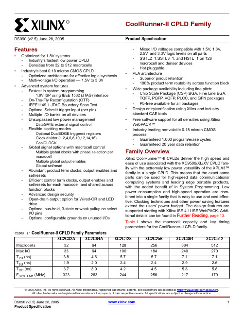
DS090 (v2.5) June 28, 1Product Specification© 2005 Xilinx, Inc. All rights reserved. All Xilinx trademarks, registered trademarks, patents, and disclaimers are as listed at /legal.htm .All other trademarks and registered trademarks are the property of their respective owners. All specifications are subject to change without notice.Features•Optimized for 1.8V systems-Industry’s fastest low power CPLD -Densities from 32 to 512 macrocells •Industry’s best 0.18 micron CMOS CPLD-Optimized architecture for effective logic synthesis -Multi-voltage I/O operation — 1.5V to 3.3V •Advanced system features-Fastest in system programming· 1.8V ISP using IEEE 1532 (JTAG) interface -On-The-Fly Reconfiguration (OTF)-IEEE1149.1 JTAG Boundary Scan Test -Optional Schmitt trigger input (per pin)-Multiple I/O banks on all devices-Unsurpassed low power management·DataGATE external signal control -Flexible clocking modes·Optional DualEDGE triggered registers ·Clock divider (÷ 2,4,6,8,10,12,14,16)·CoolCLOCK-Global signal options with macrocell control·Multiple global clocks with phase selection permacrocell ·Multiple global output enables ·Global set/reset-Abundant product term clocks, output enables andset/resets-Efficient control term clocks, output enables andset/resets for each macrocell and shared across function blocks-Advanced design security-Open-drain output option for Wired-OR and LEDdrive-Optional bus-hold, 3-state or weak pullup on selectI/O pins-Optional configurable grounds on unused I/Os-Mixed I/O voltages compatible with 1.5V, 1.8V, 2.5V, and 3.3V logic levels on all parts -SSTL2_1,SSTL3_1, and HSTL_1 on 128macrocell and denser devices -Hot pluggable •PLA architecture-Superior pinout retention-100% product term routability across function block •Wide package availability including fine pitch:-Chip Scale Package (CSP) BGA, Fine Line BGA,TQFP , PQFP , VQFP , PLCC, and QFN packages -Pb-free available for all packages•Design entry/verification using Xilinx and industry standard CAE tools•Free software support for all densities using Xilinx WebPACK™•Industry leading nonvolatile 0.18 micron CMOS process-Guaranteed 1,000 program/erase cycles -Guaranteed 20 year data retention Family OverviewXilinx CoolRunner™-II CPLDs deliver the high speed and ease of use associated with the XC9500/XL/XV CPLD fam-ily with the extremely low power versatility of the XPLA3™family in a single CPLD. This means that the exact same parts can be used for high-speed data communications/computing systems and leading edge portable products,with the added benefit of In System Programming. Low power consumption and high-speed operation are com-bined into a single family that is easy to use and cost effec-tive. Clocking techniques and other power saving features extend the users’ power budget. The design features are supported starting with Xilinx ISE 4.1i ISE WebPACK. Addi-tional details can be found in Further Reading , page 13.Table 1 shows the macrocell capacity and key timing parameters for the CoolRunner-II CPLD family.CoolRunner-II CPLD FamilyDS090 (v2.5) June 28, 2005Product SpecificationTable 1: CoolRunner-II CPLD Family ParametersXC2C32AXC2C64AXC2C128XC2C256XC2C384XC2C512Macrocells 3264128256384512Max I/O 3364100184240270T PD (ns) 3.8 4.6 5.7 5.77.17.1T SU (ns) 1.9 2.0 2.4 2.4 2.9 2.6T CO (ns) 3.73.94.24.55.85.8F SYSTEM1 (MHz)323 263 244256 217 179元器件交易网2DS090 (v2.5) June 28, 2005Product SpecificationTable 2 shows key DC characteristics for the CoolRunner-II family.Table 3 shows the CoolRunner-II CPLD package offering with corresponding I/O count. All packages are surface mount, with over half of them being ball-grid technologies.The ultra tiny packages permit maximum functional capacity in the smallest possible area. The CMOS technology used in CoolRunner-II CPLDs generates minimal heat, allowing the use of tiny packages during high-speed operation.With the exception of the new Pb-free QF packages, there are at least two densities present in each package with three in the VQ100 (100-pin 1.0mm QFP) and TQ144(144-pin 1.4mm QFP), and in the FT256 (256-ball 1.0mm spacing FLBGA). The FT256 is particularly important for slim dimensioned portable products with mid- to high-den-sity logic requirements.Table 4 details the distribution of advanced features across the CoolRunner-II CPLD family. The family has uniform basic features with advanced features included in densities where they are most useful. For example, it is very unlikely that four I/O banks are needed on 32 and 64 macrocellparts, but very likely they are for 384 and 512 macrocell parts. The I/O banks are groupings of I/O pins using any one of a subset of compatible voltage standards that share the same V CCIO level. (See Table 5 for a summary of CoolRunner-II I/O standards.)Table 2: CoolRunner-II CPLD DC CharacteristicsXC2C32AXC2C64AXC2C128XC2C256XC2C384XC2C512I CC (µA), 0 MHz, 25°C (typical)161719212325I CC (mA), 50 MHz, 70°C (max)2.5510274555CC Table 3: CoolRunner-II CPLD Family Packages and I/O CountXC2C32XC2C32AXC2C64XC2C64AXC2C128XC2C256XC2C384XC2C512QFG32(1)21------PC4433333333----PCG44(1)3333----VQ4433333333----VQG44(1)3333----QFG48(1)---37----CP5633334545----CPG56(1)3345----VQ100--64648080--VQG100(1)--648080--CP132----100106--CPG132(1)----100106--TQ144----100118118-TQG144(1)----100118118-PQ208-----173173173PQG208(1)-----173173173FT256-----184212212FTG256(1)-----184212212FG324------240270FGG324(1)------240270Notes:1.The letter "G" as the third character indicates a Pb-free package.DS090 (v2.5) June 28, 3Product SpecificationArchitecture DescriptionCoolRunner-II CPLD is a highly uniform family of fast, lowpower CPLDs. The underlying architecture is a traditional CPLD architecture combining macrocells into Function Blocks (FBs) interconnected with a global routing matrix,the Xilinx Advanced Interconnect Matrix (AIM). The Func-tion Blocks use a Programmable Logic Array (PLA) config-uration which allows all product terms to be routed and shared among any of the macrocells of the FB. Design soft-ware can efficiently synthesize and optimize logic that is subsequently fit to the FBs and connected with the ability to utilize a very high percentage of device resources. Design changes are easily and automatically managed by the soft-ware, which exploits the 100% routability of the Program-mable Logic Array within each FB. This extremely robustbuilding block delivers the industry’s highest pinout reten-tion, under very broad design conditions. The architecture will be explained by expanding the detail as we discuss the underlying Function Blocks, logic and interconnect.The design software automatically manages these device resources so that users can express their designs using completely generic constructs without knowledge of these architectural details. More advanced users can take advan-tage of these details to more thoroughly understand the software’s choices and direct its results.Figure 1 shows the high-level architecture whereby Func-tion Blocks attach to pins and interconnect to each other within the internal interconnect matrix. Each FB contains 16macrocells. The BSC path is the JTAG Boundary Scan Con-Table 4: CoolRunner-II CPLD Family FeaturesXC2C32XC2C32AXC2C64 XC2C64AXC2C128XC2C256XC2C384XC2C512IEEE 1532✓✓✓✓✓✓✓✓I/O banks 12122244Clock division ----✓✓✓✓DualEDGE Registers ✓✓✓✓✓✓✓✓DataGATE ----✓✓✓✓LVTTL✓✓✓✓✓✓✓✓LVCMOS33, 25, 18, and 15(1)✓✓✓✓✓✓✓✓SSTL2_1----✓✓✓✓SSTL3_1----✓✓✓✓HSTL_1----✓✓✓✓Configurable ground ✓✓✓✓✓✓✓✓Quadruple data security✓✓✓✓✓✓✓✓Open drain outputs ✓✓✓✓✓✓✓✓Hot plugging ✓✓✓✓✓✓✓✓Schmitt Inputs✓✓✓✓✓✓✓✓4DS090 (v2.5) June 28, 2005Product Specificationtrol path. The BSC and ISP block has the JTAG controller and In-System Programming Circuits.Function BlockThe CoolRunner-II CPLD Function Blocks contain 16 mac-rocells, with 40 entry sites for signals to arrive for logic cre-ation and connection. The internal logic engine is a 56product term PLA. All Function Blocks, regardless of the number contained in the device, are identical. For a high-level view of the Function Block, see Figure 2.At the high level, it is seen that the product terms (p-terms)reside in a programmable logic array (PLA). This structureis extremely flexible, and very robust when compared to fixed or cascaded product term function blocks.Classic CPLDs typically have a few product terms available for a high-speed path to a given macrocell. They rely on capturing unused p-terms from neighboring macrocells to expand their product term tally, when needed. The result of this architecture is a variable timing model and the possibil-ity of stranding unusable logic within the FB.The PLA is different — and better. First, any product term can be attached to any OR gate inside the FB macrocell(s).Second, any logic function can have as many p-terms as needed attached to it within the FB, to an upper limit of 56.Third, product terms can be re-used at multiple macrocell OR functions so that within a FB, a particular logical product need only be created once, but can be re-used up to 16times within the FB. Naturally, this plays well with the fitting software, which identifies product terms that can be shared. The software places as many of those functions as it can into FBs, so it happens for free. There is no need to force macrocell functions to be adjacent or any other restriction save residing in the same FB, which is handled by the soft-ware. Functions need not share a common clock, common set/reset or common output enable to take full advantage of the PLA. Also, every product term arrives with the same time delay incurred. There are no cascade time adders for putting more product terms in the FB. When the FB product term budget is reached, there is a small interconnect timing penalty to route signals to another FB to continue creating logic. Xilinx design software handles all this automatically.Figure 1: CoolRunner-II CPLD ArchitectureFigure 2: CoolRunner-II CPLD Function BlockDS090 (v2.5) June 28, 5Product SpecificationMacrocellThe CoolRunner-II CPLD macrocell is extremely efficient and streamlined for logic creation. Users can develop sum of product (SOP) logic expressions that comprise up to 40inputs and span 56 product terms within a single function block. The macrocell can further combine the SOP expres-sion into an XOR gate with another single p-term expres-sion. The resulting logic expression’s polarity is also selectable. As well, the logic function can be pure combina-torial or registered, with the storage element operating selectably as a D or T flip-flop, or transparent latch. Avail-able at each macrocell are independent selections of glo-bal, function block level or local p-term derived clocks, sets,resets, and output enables. Each macrocell flip-flop is con-figurable for either single edge or DualEDGE clocking, pro-viding either double data rate capability or the ability to distribute a slower clock (thereby saving power). For single edge clocking or latching, either clock polarity may be selected per macrocell. CoolRunner-II macrocell details are shown in Figure 3. Note that in Figure 4, standard logic symbols are used except the trapezoidal multiplexers have input selection from statically programmed configuration select lines (not shown). Xilinx application note XAPP376gives a detailed explanation of how logic is created in the CoolRunner-II CPLD family.When configured as a D-type flip-flop, each macrocell has an optional clock enable signal permitting state hold while a clock runs freely. Note that Control Terms (CT) are available to be shared for key functions within the FB, and are gener-ally used whenever the exact same logic function would be repeatedly created at multiple macrocells. The CT product terms are available for FB clocking (CTC), FB asynchro-nous set (CTS), FB asynchronous reset (CTR), and FB out-put enable (CTE).Any macrocell flip-flop can be configured as an input regis-ter or latch, which takes in the signal from the macrocell’s I/O pin, and directly drives the AIM. The macrocell combina-tional functionality is retained for use as a buried logic node if needed. F Toggle is the maximum clock frequency to which a T flip-flop can reliably toggle.Advanced Interconnect Matrix (AIM)The Advanced Interconnect Matrix is a highly connected low power rapid switch. The AIM is directed by the software to deliver up to a set of 40 signals to each FB for the cre-ation of logic. Results from all FB macrocells, as well as, all pin inputs circulate back through the AIM for additional con-nection available to all other FBs as dictated by the designFigure 3: CoolRunner-II CPLD MacrocellDS090 (v2.5) June 28, 2005Product Specificationsoftware. The AIM minimizes both propagation delay and power as it makes attachments to the various FBs.I/O BlockI/O blocks are primarily transceivers. However, each I/O is either automatically compliant with standard voltage ranges or can be programmed to become so. See XAPP382 for detailed information on CoolRunner-II I/Os.In addition to voltage levels, each input can selectively arrive through Schmitt-trigger inputs. This adds a small time delay, but substantially reduces noise on that input pin.Approximately 500 mV of hysteresis will be added when Schmitt-trigger inputs are selected. All LVCMOS inputs can have hysteresis input. Hysteresis also allows easy genera-tion of external clock circuits. The Schmitt-trigger path is best seen in Figure 4. See Table 5 for Schmitt-trigger com-patibility with I/O standards.Outputs can be directly driven, 3-stated or open-drain con-figured. A choice of slow or fast slew rate output signal isalso available. Table 5 summarizes various supported volt-age standards associated with specific part capacities. All inputs and disabled outputs are voltage tolerant up to 3.3V.The CoolRunner-II family supports SSTL2-1, SSTL3-1 and HSTL-1 high-speed I/O standards in the 128-macrocell and larger devices. Figure 4 details the I/O pin, where it is noted that the inputs requiring comparison to an external refer-ence voltage are available. These I/O standards all require VREF pins for proper operation. The CoolRunner-II CPLD allows any I/O pin to act as a VREF pin, granting the board layout engineer extra freedom when laying out the pins.However, if VREF pin placement is not done properly,additional VREF pins may be required, resulting in a loss of potential I/O pins or board re-work. See XAPP399 for details regarding VREF pins and their placement.V REF has pin-range requirements that must be observed.The Xilinx software aids designers in remaining within the proper pin range.Table 5 summarizes the single ended I/O standard support and shows which standards require V REF values and board termination. V REF detail is given in specific data sheets.Figure 4: CoolRunner-II CPLD I/O Block DiagramTable 5: CoolRunner-II CPLD I/O Standard SummaryIOSTANDARD Attribute V CCIO Input V REFBoard Termination Voltage(V TT )Schmitt-trigger SupportLVTTL 3.3 N/A N/A Optional LVCMOS33 3.3 N/A N/A Optional LVCMOS25 2.5 N/A N/A Optional LVCMOS18 1.8 N/A N/A Optional LVCMOS15 1.5 N/A N/A Not optional HSTL_1 1.5 0.75 0.75Not optional SSTL2_1 2.5 1.25 1.25Not optional SSTL3_13.31.51.5Not optionalDS090 (v2.5) June 28, 7Product SpecificationOutput BankingCPLDs are widely used as voltage interface translators. To that end, the output pins are grouped in large banks. The XC2C32 and XC2C64 devices are not banked, but the new XC2C32A and XC2C64A devices have two banks. The medium parts (128 and 256 macrocell) support two output banks. With two, the outputs will switch to one of two selected output voltage levels, unless both banks are set to the same voltage. The larger parts (384 and 512 macrocell)support four output banks split evenly. They can support groupings of one, two, three or four separate output voltage levels. This kind of flexibility permits easy interfacing to 3.3V, 2.5V, 1.8V, and 1.5V in a single part.DataGATELow power is the hallmark of CMOS technology. Other CPLD families use a sense amplifier approach to creating product terms, which always has a residual current compo-nent being drawn. This residual current can be several hun-dred milliamps, making them unusable in portable systems.CoolRunner-II CPLDs use standard CMOS methods to cre-ate the CPLD architecture and deliver the corresponding low current consumption, without doing any special tricks.However, sometimes designers would like to reduce their system current even more by selectively disabling circuitry not being used.The patented DataGATE technology was developed to per-mit a straightforward approach to additional power reduc-tion. Each I/O pin has a series switch that can block the arrival of free running signals that are not of interest. Sig-nals that serve no use may increase power consumption,and can be disabled. Users are free to do their design, then choose sections to participate in the DataGATE function.DataGATE is a logic function that drives an assertion rail threaded through the medium and high-density CoolRunner-II CPLD parts. Designers can select inputs to be blocked under the control of the DataGATE function,effectively blocking controlled switching signals so they do not drive internal chip capacitances. Output signals that do not switch, are held by the bus hold feature. Any set of input pins can be chosen to participate in the DataGATE function.Figure 5 shows the familiar CMOS I CC versus switching fre-quency graph. With DataGATE, designers can approach zero power, should they choose to, in their designs Figure 6 shows how DataGATE basically works. One I/O pin drives the DataGATE Assertion Rail. It can have any desired logic function on it. It can be as simple as mapping an input pin to the DataGATE function or as complex as a counter or state machine output driving the DataGATE I/O pin through a macrocell. When the DataGATE rail is asserted high, any pass transistor switch attached to it is blocked. Note that each pin has the ability to attach to theAIM through a DataGATE pass transistor, and thus be blocked. A latch automatically captures the state of the pin when it becomes blocked. The DataGATE Assertion Rail threads throughout all possible I/Os, so each can participate if chosen. Note that one macrocell is singled out to drive the rail, and that macrocell is exposed to the outside world through a pin, for inspection. If DataGATE is not needed,this pin is an ordinary I/O.Figure 5: CMOS I CC vs. Switching Frequency CurveDS090 (v2.5) June 28, 2005Product SpecificationGlobal SignalsGlobal signals, clocks (GCK), sets/resets (GSR) and output enables (GTS), are designed to strongly resemble each other. This approach enables design software to make the best utilization of their capabilities. Each global capability is supplemented by a corresponding product term version.Figure 7 shows the common structure of the global signal trees. The pin input is buffered, then drives multiple internal global signal traces to deliver low skew and reduce loading delays. The DataGATE assertion rail is also a global signal.Additional Clock Options: Division, DualEDGE, and CoolCLOCKDivisionCircuitry has been included in the CoolRunner-II CPLD architecture to divide one externally supplied global clock by standard values. Division by 2,4,6,8,10, 12, 14 and 16are the options (see Figure 8). This capability is supplied on the GCK2 pin. The resulting clock produced will be 50%duty cycle for all possible divisions. Note that a Synchro-nous Reset (CDRST) is included to guarantee no runt clocks can get through to the global clock nets. Note that again, the signal is buffered and driven to multiple traces with minimal loading and skew.DualEDGEEach macrocell has the ability to double its input clock switching frequency. Figure 9 shows the macrocell flip-flop with the DualEDGE option (doubled clock) at each macro-cell. The source to double can be a control term clock, a product term clock or one of the available global clocks. The ability to switch on both clock edges is vital for a number of synchronous memory interface applications as well as cer-tain double data rate I/O applications.Figure 6: DataGATE Architecture (output drivers not shown)Figure 7: Global Clocks (GCK), Sets/Resets (GSR) andOutput Enables (GTS)DS090 (v2.5) June 28, 9Product SpecificationCoolCLOCKIn addition to the DualEDGE flip-flop, additional power sav-ings can be had by combining the clock division circuitry with the DualEDGE circuitry. This capability is called Cool-CLOCK and is designed to reduce clocking power within the CPLD. Because the clock net can be an appreciable powerdrain, the clock power can be reduced by driving the net at half frequency, then doubling the clock rate using DualEDGE triggering at the macrocells. Figure 10 shows how CoolCLOCK is created by internal clock cascading with the divider and DualEDGE flip-flop working together. See XAPP378 for more detail.Figure 8: Clock Division Circuitry for GCK2Figure 9: Macrocell Clock Chain with DualEDGE Option ShownFigure 10: CoolCLOCK Created by Cascading Clock Divider and DualEDGE OptionDS090 (v2.5) June 28, 2005Product SpecificationDesign SecurityDesigns can be secured during programming to prevent either accidental overwriting or pattern theft via readback.Four independent levels of security are provided on-chip,eliminating any electrical or visual detection of configuration patterns. These security bits can be reset only by erasing the entire device. See WP170 for more detail.Timing ModelFigure 11 shows the CoolRunner-II CPLD timing model. It represents one aspect of the overall architecture from a tim-ing viewpoint. Each little block is a time delay that a signal will incur if the signal passes through such a resource. Tim-ing reports are created by tallying the incremental signal delays as signals progress within the CPLD. Software cre-ates the timing reports after a design has been mapped onto the specific part, and knows the specific delay values for a given speed grade. Equations for the higher level tim-ing values (i.e., T PD and F SYSTEM ) are available. Table 6summarizes the individual parameters and provides a brief definition of their associated functions.Xilinx application note XAPP375 details the CoolRunner-II CPLD family tim-ing with several examples.Figure 11: CoolRunner-II CPLD Timing ModelTable 6: Timing Parameter Definitions Symbol ParameterBuffer DelaysT lN Input Buffer DelayT DIN Direct data register input delay T GCK Global clock (GCK) buffer delay T GSR Global set/reset (GSR) buffer delay T GTS Global output enable (GTS) buffer delay T OUT Output buffer delayT EN Output buffer enable/disable delay T SLEW Output buffer slew rate control delay P-term Delays T CT Control Term delay (single PT or FB-CT)T LOGI1Single P-term logic delay T LOGI2Multiple P-term logic delay adderMacrocell DelaysT PDI Macro cell input to output valid T SUI Macro register setup before clock T HI Macro register hold after clock T ECSU Macro register enable clock setup time T ECHO Macro register enable clock hold time T COI Macro register clock to output valid T AOI Macro register set/reset to output valid T HYS Hysteresis selection delay adder Feedback DelaysT F Feedback delayT OEMMacrocell to Global OE delayTable 6: Timing Parameter Definitions (Continued)Symbol ParameterProgrammingThe programming data sequence is delivered to the device using either Xilinx iMPACT software and a Xilinx download cable, a third-party JTAG development system, a JTAG-compatible board tester, or a simple microprocessor interface that emulates the JTAG instruction sequence. The iMPACT software also outputs serial vector format (SVF) files for use with any tools that accept SVF format, including automatic test equipment. See CoolRunner-II Application Notes for more information on how to program.In System ProgrammingAll CoolRunner-II CPLD parts are 1.8V in system program-mable. This means they derive their programming voltage and currents from the 1.8V V CC (internal supply voltage) pins on the part. The V CCIO pins do not participate in this operation, as they may assume another voltage ranging as high as 3.3V down to 1.5V. A 1.8V V CC is required to prop-erly operate the internal state machines and charge pumps that reside within the CPLD to do the nonvolatile program-ming operations. The JTAG interface buffers are powered by a dedicated power pin, V CCAUX, which is independent of all other supply pins. V CCAUX must be connected. Xilinx software is provided to deliver the bit-stream to the CPLD and drive the appropriate IEEE 1532 protocol. To that end, there is a set of IEEE 1532 commands that are supported in the CoolRunner-II CPLD parts. Programming times are less than one second for 32 to 256 macrocell parts. Program-ming times are less than four seconds for 384 and 512 mac-rocell parts. Programming of CoolRunner-II CPLDs is only guaranteed when operating in the commercial temperature and voltage ranges as defined in the device-specific data sheets.On-The-Fly Reconfiguration (OTF)Xilinx ISE 5.2i supports OTF for CoolRunner-II CPLDs. This permits programming a new nonvolatile pattern into the part while another pattern is currently in use. OTF has the same voltage and temperature specifications as system program-ming. During pattern transition I/O pins are in high imped-ance with weak pullup to V CCIO. Transition time typically lasts between 50 and 300 µs, depending on density. See XAPP388 for more information.JTAG InstructionsTable7 shows the commands available to users. These same commands may be used by third party ATE products,as well. The internal controllers can operate as fast as 66 MHz.Power-Up CharacteristicsCoolRunner-II CPLD parts must operate under the demands of both the high-speed and the portable market places, therefore, they must support hot plugging for the high-speed world and tolerate most any power sequence to its various voltage pins. They must also not draw excessive current during power-up initialization. To those ends, the general behavior is summarized as follows:1.I/O pins are disabled until the end of power-up.2.As supply rises, configuration bits transfer fromnonvolatile memory to SRAM cells.3.As power up completes, the outputs become asconfigured (input, output, or I/O).4.For specific configuration times and power uprequirements, see the device specific data sheet. CoolRunner-II CPLD I/O pins are well behaved under all operating conditions. During power-up, CoolRunner-II devices employ internal circuitry which keeps the devices in the quiescent state until the V CCINT supply voltage is at a safe level (approximately 1.3V). In the quiescent state, JTAG pins are disabled, and all device outputs are disabled with the pins weakly pulled high, as shown in Table8. When the supply voltage reaches a safe level, all user registers become initialized, and the device is immediately available for operation, as shown in Figure12. Best results are obtained with a smooth V CC rise in less than 4 ms. Final V CC value should occur within 1 second.If the device is in the erased state (before any user pattern is programmed), the device outputs remain disabled with a weak pull-up. The JTAG pins are enabled to allow the Table 7: JTAG InstructionsCode Instruction Description 00000000EXTEST Force boundary scan data ontooutputs00000011PRELOAD Latch macrocell data intoboundary scan cells11111111BYPASS Insert bypass register betweenTDI and TDO00000010INTEST Force boundary scan data ontoinputs and feedbacks 00000001IDCODE Read IDCODE11111101USERCODE Read USERCODE11111100HIGHZ Force output into highimpedance state11111010CLAMP Latch present output state。
SGM3002中文资料
PIN DESCRIPTION
NAME
SC70-6 PIN
V+
2
GND
3
IN(IN1, IN2)
1
COM(COM1, COM2)
5
NO(NO1, NO2)
6
NC(NC1, NC2)
4
MSOP-10 PIN
8 3
1,5
6,10 2,4 7,9
FUNCTION
Power supply Ground Digital control pin to connect the COM terminal to the NO or NC terminals Common terminal Normally-open terminal Normally-closed terminal
Stresses beyond those listed under “Absolute Maximum Ratings” may cause permanent damage to the device. These are stress ratings only, and functional operation of the device at these or any other conditions beyond those indicated in the operational sections of the specifications is not implied. Exposure to absolute maximum rating conditions for extended periods may affect device reliability. (1) Signals on NC, NO, or COM or IN exceeding V+ will be clamped by internal diodes. Limit forward diode current to maximum current ratings.
电子元器件采购网站_万联芯城

电子元器件采购网站
万联芯城专为终端客户提供一站式电子元器件配套业务,采购电子元件就上万联芯城,万联芯城电子元器件采购网站代理长电,顺络,先科ST等优质品牌电子元器件,国际品牌代理渠道进货,拥有上万种现货库存。
点击进入万联芯城
点击进入万联芯城
做电子元器件采购网站就需要许多的知识及条件才能够买到最
好的产品。
那么做电子元器件采购网站需要什么样的条件呢?首先你必须对该行业有一定的认识和把握。
对于做电子元器件采购网站的人来说,必须对该行业有深入的了解,能够掌握市场动向,这样才能变化多端的市场中及时抓住商机购买到最优质的产品
当然除此之外,电子元器件采购网站还必须具备一定的采购基础知识。
比如在采购的时候,你必须要确认供应商是否建立有一套稳定且有效的质量保障体系。
如果供应商的产品质量不合格或者不过关的话,那么就会直接影响到后续的一些工作。
如此你还应该充分了解,对该行业电子元件产品的价格有所依定的了解,具备与供应商谈论成本与价格的能力。
因为对于购买商来说公道合理的价格就能够节约不少的成本,也能够与运营商达成双赢。
最后,还必须掌握更多的供应商信息以及其他购买渠道与方法。
这样才能够对多家供应商进行比较,而选择一家自己最满意也是最了解的,我要购买到质量最高,价格最便宜的产品。
除了具备以下的一些条件之外,进行电子元器件采购网站时,还必须非常清楚地知道它的工作流程。
比如询价准备,定价格,决定供应商等。
以上一些就是做电子元器件采购网站所需要的一些条件,都充分地具备这些条件之后,才能更好的工作。
MAXIM美信代理

万联芯城-电子元器件采购网www,是国内有名的电子元器件供应商,万联芯城提供一站式电子元器件配单业务,只需提交BOM表,即可报价,当天发货,MAXIM美信半导体等进口原装现货品牌元件价格更有优势,为客户节省采购成本。
点击进入万联芯城Maxim Integrated是一家美国上市公司,设计,制造和销售模拟和混合信号集成电路。
[3]Maxim Integrated开发用于汽车,工业,通信,消费和计算市场的集成电路(IC)。
该公司总部位于加利福尼亚州圣何塞,在全球设有设计中心,制造工厂和销售办事处。
在2018财政年度,它在全球拥有24.8亿美元的销售额,8,800名员工和35,000名客户。
[4] Maxim 是纳斯达克100指数,罗素1000指数和MSCI美国指数上市的财富1000强公司。
MAXIM代理,美信代理成立于1983年4月。
[5]其九名初始团队成员在半导体设计和销售方面拥有丰富的经验。
创始团队包括自20世纪60年代以来的行业先驱杰克吉福德; Fred Beck,IC销售和分销先驱;戴维宾汉姆,1982年通用电气年度科学家; Steve Combs,晶圆技术和制造的先驱; Lee Evans,也是CMOS模拟微芯片设计的先驱,也是1982年通用电气的年度科学家; Dave Fullagar,个内部补偿运算放大器电路的发明者; Roger Fuller,CMOS芯片设计的又一先驱; Rich Hood,一些微处理器控制半导体测试系统的开发总监;和Dick Wilenken,他被公认为关键模拟开关和多路复用器技术之父。
[6]根据两页的商业计划,他们获得了900万美元的风险投资来建立公司。
[7]在年,该公司开发了24个第二源产品。
之后,MAXIM代理,美信代理设计的专利产品可以提供更大的差异化和更高的利润。
1985年,业界推出了MAX600,这是个获得行业奖项并开始数十年技术创新的专利产品。
MAXIM代理,美信代理在1987年的个盈利财政年度,在一个名为MAX232的产品的帮助下,自1988年上市以来每年都实现盈利。
TOP244Y中文资料

®
+ DC OUT -
D
L
CONTROL
TOPSwitch-GX
S X F
C
PI-2632-060200
ቤተ መጻሕፍቲ ባይዱ
Figure 1. Typical Flyback Application.
OUTPUT POWER TABLE
230 VAC ±15%4 85-265 VAC Adapter1 Open Frame2
6.5 W 7W 7W 9W 15 W 15 W 11 W 18 W 20 W 20 W 26 W 24 W 40 W 26 W 55 W 28 W 70 W 30 W 80 W
10 W 14 W 14 W 15 W 23 W 30 W 20 W 28 W 45 W 32 W 60 W 36 W 90 W 43 W 125 W 48 W 155 W 52 W 180 W
Table 1. Notes: 1. Typical continuous power in a non-ventilated enclosed adapter measured at 50 °C ambient. Assumes 1 sq. in. of 2 oz. copper heat sink area for R package. 2. Maximum practical continuous power in an open frame design at 50 °C ambient. See Key Applications for detailed conditions. Assumes 3 sq. in. of 2 oz. copper heat sink area for R package. 3. See Part Ordering Information. 4. 230 VAC or 100/115 VAC with doubler.
TL032中文资料

元器件交易网IMPORTANT NOTICETexas Instruments (TI) reserves the right to make changes to its products or to discontinue any semiconductorproduct or service without notice, and advises its customers to obtain the latest version of relevant informationto verify, before placing orders, that the information being relied on is current.TI warrants performance of its semiconductor products and related software to the specifications applicable atthe time of sale in accordance with TI’s standard warranty. Testing and other quality control techniques areutilized to the extent TI deems necessary to support this warranty. Specific testing of all parameters of eachdevice is not necessarily performed, except those mandated by government requirements.Certain applications using semiconductor products may involve potential risks of death, personal injury, orsevere property or environmental damage (“Critical Applications”).TI SEMICONDUCTOR PRODUCTS ARE NOT DESIGNED, INTENDED, AUTHORIZED, OR WARRANTEDTO BE SUITABLE FOR USE IN LIFE-SUPPORT APPLICATIONS, DEVICES OR SYSTEMS OR OTHERCRITICAL APPLICATIONS.Inclusion of TI products in such applications is understood to be fully at the risk of the customer. Use of TIproducts in such applications requires the written approval of an appropriate TI officer. Questions concerningpotential risk applications should be directed to TI through a local SC sales office.In order to minimize risks associated with the customer’s applications, adequate design and operatingsafeguards should be provided by the customer to minimize inherent or procedural hazards.TI assumes no liability for applications assistance, customer product design, software performance, orinfringement of patents or services described herein. Nor does TI warrant or represent that any license, eitherexpress or implied, is granted under any patent right, copyright, mask work right, or other intellectual propertyright of TI covering or relating to any combination, machine, or process in which such semiconductor productsor services might be or are used.Copyright © 1996, Texas Instruments Incorporated。
中国各行业的行业网站

箱包资源
美国箱包品牌网
美国时尚包袋网
加拿大箱包协会
服际名品服饰网
中国内衣网
世界时装网
浙江服装网
中国服装协会
中国服装网
服装、鞋帽市场·阿里..
中国服装服饰商贸网
广东服装网
美国服装网
中国服装销售网
中华服装网
美国服装商会
中国纺织服装信息网
中国纺织面料网
中国纺织服装网
中国建筑装饰网
国家建材网
中国智能建筑信息网
中国土木
钢材信息网
中国玻璃行业信息网
中国建筑材料价格网
中国照明信息网
中国石材总网
中华建材网
西部建材网
中国水泥网
中国瓷砖网
中国陶瓷网
中国瓷网
中国防水网
建材
武汉装饰建材网
盈拓国际建材展览网
中华建材在线
中国门业在线
千居建材装潢信息网
中华人民共和国建设部
中国建材报
中国防水协会
169鞋业资讯网
中华皮革网
中国鞋业互联网
中国晋江鞋网
中国皮革网
中华鞋业
万亿皮革商务网
中国皮鞋网
中国台州鞋网
中华皮革在线
中国鞋垫网
中国鞋业网
GOOGLE搜索引擎
中国服装服饰商贸网
中国服装机械网
国际服饰交易网
服饰商情
长三角服饰在线集散中心
中国国际服装网
中华服饰网
中华服饰商贸网
联科绣花网
中华内衣网
中国服饰批发网
陕西西府民间工艺品网
56民族文化网
银邑纯银饰品空间
中国56民族工艺品网
云南民族工艺品网
stm32f103rbt6中文资料_数据手册_参数
万联芯城wwwwlxmallcom电子元器件采购网提供一站式配套解决物料烦恼万联芯城以良心做好良芯专为终端工厂企业客户提供电子元器件一站式配套报价服务客户提交物料清单商城即可整单报价整单下单有优惠万联芯城拥有完善的产品供应链体系及现代化仓储系统可满足多种bom报价需求点击进入万联芯城
万联芯城-电子元器件采购网,提供一站式配套,解决 物料烦恼,万联芯城-以良心做好良芯,专为终端工厂企业客户提供电 子元器件一站式配套报价服务,客户提交物料清单,商城即可整单报价, 整单下单有优惠,万联芯城拥有完善的产品供应链体系及现代化仓储系统 ,可满足多种BOM报价需求,点击进入万联芯城。
描述 STM32F103x8,STM32F103xB一百〇五分之一十八 DocID13587 Rev 16高级控制定时器(TIM1)高级控制定时器(TIM1) 可以看作是6路三相PWM复用通道.它具有互补的PWM输出,具有可编程的插入死区.它也可以看作是一个完整的通用定时器. 4个独立通道可以用于 ?输入捕捉 ?输出比较 ? PWM生成(边沿或中心对齐模式) ?单脉冲模式输出如果配置为通用16位定时 器,它具有与TIMx定时器相同的功能.如果配置为16位PWM发生器,具有完全调制能力(0-100%).在调试模式下,高级控制 定时器计数器可以被冻结,PWM输出禁用这些输出驱动的任何电源开关.许多功能与具有该功能的通用TIM定时器共享相同的 建筑.因此,高级控制定时器可以与TIM一起工作定时器通过定时器链接功能进行同步或事件链接.通用计时器(TIMx)多可以 嵌入三个可同步的通用定时器 STM32F103xx性能线设备.这些定时器基于16位自动重新加载一个16位预分频器,具有4个独立的 通道,用于输入捕捉/输出比较,PWM或单脉冲模式输出.多可输入12个输入捕获/输出比较/大封装上的PWM.通用定时器可以 通过定时器与高级控制定时器一起工作用于同步或事件链接的链接功能.他们的计数器可以在调试中冻结模式.任何通用定时器 都可用于产生PWM输出.他们都具有独立的DMA请求生成.这些定时器能够处理正交(增量)编码器信号 1到3个霍尔效应传感 器的数字输出.独立看门狗独立看门狗基于12位向下计数器和8位预分频器.它是来自独立的40 kHz内部RC,并且它独立于运行 主时钟,它可以在停止和待机模式下工作.它可以用作看门狗在发生问题时重置设备,或者作为应用程序超时的自由运行定时 器管理.它可以通过选项字节进行硬件或软件配置.柜台可以在调试模式下冻结.窗口看门狗窗口看门狗基于可以设置为自由运 行的7位下行计数器.它可以用作看门狗在出现. DocID13587 Rev 16 2.3概观 2.3.1 具有嵌入式闪存和SRAM的ARM?Cortex?-M3内核 ARM Cortex?-M3处理器是嵌入式的新一代 ARM处理器系统.它已经开发出来提供一个满足MCU需求的低成本平台实现,减少引脚数和低功耗,同时交付出色的计算性 能和对中断的高级系统响应. ARM Cortex?-M3 32位RISC处理器具有卓越的代码效率,通过ARM内核提供高性能预期的内存大 小与8位和16位器件相关联.因此,具有嵌入式ARM内核的STM32F103xx性能系列产品系列兼容所有ARM工具和软件.图1显示了 器件系列的一般框图. 2.3.2嵌入式闪存 64或128 KB的嵌入式闪存可用于存储程序和数据. 2.3.3 CRC(循环冗余校验)计算单元 CRC(循环冗余校验)计算单元用于从32位获取CRC码数据字和固定的生成多项式.在其他应用中,基于CRC的技术用于验证 数据传输存储完整性.在EN / IEC 60335-1标准的范围内,它们提供了一种方法验证闪存完整性. CRC计算单元有助于计算签名 在运行期间的软件,与链接时生成的参考签名进行比较,时间并存储在给定的存储位置. 2.3.4嵌入式SRAM以0等待的CPU时钟 速度访问(读/写)二十KB的嵌入式SRAM状态. 2.3.5嵌套矢量中断控制器(NVIC) STM32F103xx性能线嵌入一个嵌套向量中 断控制器处理多达43个可屏蔽中断通道(不包括16个中断线 Cortex?-M3)和16个优先级. ?紧密耦合的NVIC提供低延迟中断处 理 ?中断条目向量表地址直接传递给核心 ?紧密耦合的NVIC核心接口 ?允许早期处理中断 ?处理晚到高优先级中断 ?支持尾链 ? 处理器状态自动保存 ?中断条目在中断退出时恢复. DMA灵活的7通道通用DMA能够管理内存到内存,外设到内存和内存到外设的传输. DMA控制器支持循环缓冲管理避免了当 控制器产生中断到达缓冲区的末尾.每个通道都连接到专用硬件DMA请求,并支持软件触发每个通道.配置由软件和传输大小 之间进行源和目的地是独立的. DMA可用于主要外设:SPI,I 2 C,USART,通用和高级控制定时器TIMx和ADC. 2.3.14 RTC(实时时钟)和备份寄存器 RTC和备用寄存器是通过开启电源的开关提供的 V DD 电源存在或通过V BAT 引脚. 备份寄存 器是十个16位 当V DD 电源不存在 时,寄存器用于存储20个字节的用户应用数据 .实时时钟提供了一套连续运行的计数器,可 与之配合使用适合软件提供时钟日历功能,并提供报警中断和周期性中断.它采用32.768 kHz外部晶振,谐振器或振荡器内部 低功耗RC振荡器或高速外部时钟除以128内部低功耗RC的典型频率为40 kHz.可以使用RTC进行校准外部512 Hz输出,以补偿 任何天然晶体偏差. RTC具有32位可编程计数器,可使用Compare进行长期测量注册以产生报警.一个20位的预分频器用于时基 时钟默认配置为从32.768 kHz的时钟生成1秒的时基. 2.3.15计时器和看门狗中密度STM32F103xx性能线设备包括高级控制定时 器,三个通用定时器,两个看门狗定时器和一个SysTick定时器.表4比较了高级控制和通用定时器的功能.表4.定时器功能比较 计时器计数器解析度计数器类型预分频器因子 DMA请求代捕获/比较渠道补充输出 TIM1 16位向上,下,向上/向下任何整数 介于1之间和65536是 4是 TIM2, TIM3, TIM4 16位向上,下,向上/向下任何整数介于1之间
- 1、下载文档前请自行甄别文档内容的完整性,平台不提供额外的编辑、内容补充、找答案等附加服务。
- 2、"仅部分预览"的文档,不可在线预览部分如存在完整性等问题,可反馈申请退款(可完整预览的文档不适用该条件!)。
- 3、如文档侵犯您的权益,请联系客服反馈,我们会尽快为您处理(人工客服工作时间:9:00-18:30)。
元器件采购网
万联芯城电子元器件采购网专售原装现货电子元器件,包含IC集成电路,二三价格,电阻电容等主动被动类元器件。
万联芯城为客户提供专业的电子元器件配单服务,提交BOM表,当天即可获得优势价格,当天即可发货,欢迎广大客户咨询,点击进入万联芯城
从现在的市场当中我们就可以知道,其实元器件采购网的兴起,也就说明了现在市场当中对于这种线上采购的一个强烈的需求,特别是大量中小型企业对于这类线上采购平台的渴求,更是使得它能够快速发展起来的一个重要的条件。
目前在电子元器件的相关市场上面,元器件采购网足足拥有着万亿级的容量,也可以说这个市场是远远还没有达到饱和的状态,更多的不同的发展,都是大有可为的,而在元器件采购网当中,其实为大家呈现出来的,就是一种各种电子元器件创新式的线上交易方式,使得众多的采购企业能够拥有着全新的体验,并且也为大家带去了更为实惠、更为方便、也更为放心的一种采购方式。
在元器件采购网当中拥有着国内外大量品牌的授权以及入驻,所以就能够很好地保证在这个网站里面,大家采购到的电子元器件都是
绝对的原厂正版的产品,使得采购人员们再也不需要想尽办法去查验真假,因为元器件采购网有着保真的条款,如果有出现假货的问题,那么都可以得到相应的赔偿,这就给大家在采购的时候,省下了很多的心力。
也是因为这一点,所以现在的元器件采购网都是拥有着很多粘性很强的客户,大部分的企业用户都会在采购过之后,成为一个长期、稳定的客户,从而使得采购网当中的商品,都可以以非常稳定的一个销售速度被不断地采购。