DAC904E中文资料
EXTRAmatic 9040 说明书

使用说明书EXTRAmatic 9040安全常伴您左右KaVo Dental GmbH Wangener Straße 78D-88299 Leutkirch++ 49 (0) 7561 86-0++ 49 (0) 7561/86-400目录1用户说明1.1用户指南1.1.1 标志1.1.2 目标对象1.1.3 缩略语1.2 服务1.3 保修条件1.4 运输和储存1.4.1 德国1998年8月28包装条例1.4.2 运输损坏1.4.3 储存2安全2.1 安全使用说明2.1.1 危险级别说明2.1.2 结构2.2 预定用途2.2.1 概述2.2.2 产品具体信息2.3 安全说明2.3.1 概述2.4 防护衣3 产品描述3.1 EXTRAmatic 前面3.2 EXTRAmatic 后面3.3 控制面板3.4 技术参数3.5铭牌4 启动4.1 试运行的准备4.1.1 搬运产品4.2 连接组件4.2.1在工作场所的连接4.2.2在牙科技工中心的连接4.2.3连接吸尘软管4.2.4 水平校准4.2.5 连接控制线4.2.6 连接导线4.2.7 连接脚踏开关4.2.8 连接外控面板4.2.9 连接电源5. 操作5.1 各程序的功用5.2用户程序5.2.1 水平面测量5.2.2 自动模式5.2.3 连续模式5.2.4预设吸尘强度等级5.3 应用程序5.3.1 应用程序按键(2000)5.3.2 “用户系统”应用程序(2050)5.3.3 “用户设定检查”应用程序(2100)5.3.4 “数字语言”应用程序(2150)5.3.5 “标准屏幕”应用程序(2800)5.3.6 “初始化存储器”应用程序(2250)5.3.7 “自动感应调节”应用程序(2300)5.3.8 “手动感应调节”应用程序(2350)5.3.9 “接口气压显示“应用程序(2400)5.3.10 “活性碳过滤器控制”应用程序(2500)5.3.11 “修改活性碳过滤器使用时间”应用程序(2450)5.3.12 “活性碳过滤器更换后所经过的时间”应用程序(2455)5.3.13 “重新设定活性碳过滤器监测时间”应用程序(2550)5.3.14 “延续工作时间”应用程序(2600)5.3.15 “记忆时间”应用程序(2650)5.3.16 “SW 版本”应用程序(2700)5.3.17 “过滤器清洁间隔时间”应用程序(2750)6 保养方法6.1 清洁6.2 维护6.2.1 更换垃圾袋6.2.2 更换活性碳过滤器6.2.3 更换长期过滤器6.2.4 警示灯7 故障检修8 附件1 用户说明1.1 用户指南要求请于首次使用本产品前,认真阅读以下说明,以避免错误操作及产品损坏。
AR904进程分析仪说明书

USER MANUALPROCESS ANALOGUE CALIBRATORAR904Version 1.1.12013.02.13Thank you for choosing our product.This user manual will help you with proper and safeoperation and full use of the process analogue calibrator device.Before installing and operating, please readand understand this manual.If you have any additional questions, please contact the technical advisor. TABLE OF CONTENTSPay special attention to information marked with this sign!Manufacturer reserves the right to make changes in design and software of the device without compromising technical parameters1.SAFETY PRECAUTIONS▪Before using the unit, please read this manual carefully.▪To avoid electrical shock or damage to the device, mechanical and electrical installation have to be performed by a qualified personnel.▪Before turning on the power make sure that all cables are properly connected.▪Before making any modifications to the wiring connections, turn off all voltages applied to the device. ▪You have to ensure proper working conditions, according to the specifications of the device (power supply voltage, humidity, temperature, chapter 5).2.INSTALLATION NOTESThis instrument was designed to provide the appropriate level of resistance to most disturbances that may occur in industrial environments. In environments with unknown level of interference it is recommended to use the following measures to prevent possible interference with operation of the instrument:▪Do not power supply the device from the same line as the power component without the appropriate network filters.▪Use only shielded power and signal cables taking into account that the grounding of the shield should bea single point, made as close to the device as possible.▪Avoid placing signal cables very close and parallel to energy and power cables.▪It is recommended to twist signal cables in pairs.▪Avoid proximity of remote controlled devices, electromagnetic meters, high power loads, loads with phase or group power control and other devices that generate large impulse disturbances.▪Ground or zero metal rails that are used to mount rail devices.Before using the device, remove the protective film from the LED display.3.GENERAL PROCESS ANALOGUE CALIBRATOR CHARACTERISTICS▪This device allows you to control or test devices with current or voltage input (proportional valves, servomotors, inverters, motors, etc.)▪ 2 analogue outputs (working simultaneously):-current 4÷20mA or 0÷20mA (active, cannot be powered from 2 wires current loop)-voltage 0÷10V▪Soft start/stop (ramping) or triangle wave generator with manual or automatic (activated after device power on) trigger.▪Programmable setpoint value, output signal change step, display range, soft start/stop options, communication options, access options and other configuration parameters.▪7-segment LED display with brightness adjustment.▪Optional RS485/RS232 serial interface (galvanically isolated, MODBUS-RTU protocol).▪Parameters configuration methods:-Using IP65 foil keyboard located on the device front panel-Using AR955 programmer or RS485/RS232 interface with PC software (Windows 2000/XP/Vista/7)▪Available free software that allows parameters configuration.▪Access to configuration parameters can be password protected.▪High accuracy and high resistance to interference.▪Available accessories:-AR955 programmer-RS485 to USB converterCAUTION:Before starting work with the process analogue calibrator, read this manual carefully and perform electrical and mechanical installation properly and set parameters correctly.4.PACKAGE CONTENTS▪Process analogue calibrator▪User manual▪Warranty card5.TECHNICAL DATA(1)- Output cannot be powered from two wires current loop6.HOUSING DIMMENSIONS AND INSTALLATION DATA7.TERMINAL STRIPS AND ELECTRICAL CONNECTIONS DESCRIPTIONa)Terminals and output signals descriptionOnly AR955 programmer can be connected to PRG socket. Connecting other devices to PRG socket can damage connected device and AR904 process analogue calibrator.8.BUTTONS DESCRIPTIONa) Buttons functions in setpoint value display mode (normal mode)) )and 9: b) Buttons functions in parameters configuration mode (chapter 10)9.OUTPUTS SETPOINT VALUE CHANGEPressing [UP] or [DOWN] button while setpoint value is being displayed will change the value by pre-set step(parameter 6: , chapter 10, table 10). Changes of the output signal are proportional to changes of the displayed value. Pressing [SET] + [DOWN] buttons together will set output value immediately to lower rangevalue (2: or 4: ) while pressing [SET] + [UP] buttons together will set output value immediately to upperrange value (3: or 5: ). In addition, the output signal may be given also in parameters programming mode(parameter 7: ) and using serial interface RS485/RS232 or AR955 programmer (chapter 15, table 15). Moreover, it is possible to set the setpoint value outside of the display range based on the parameters 2: and 3:. The value of this override that can be set using the buttons is ±5% for 4÷20mA (2÷10V) output and 6,2% for the remaining outputs.10.CONFIGURATION PARAMETERS SETUPAll configuration parameters of the device are saved in the non-volatile EEPROM internal memory. Two parameters configuration methods are available:ing IP65 foil keyboard located on the front panel of the device:-From the setpoint value display mode enter configuration menu (press and hold for more than 1 second [UP] and [DOWN] buttons together). If parameter 13: (password protection is turned on), display will show message and then with first digit blinking. Using [UP] or [DOWN] button enter protection password (by default parameter 12: ). To proceed to the next digit or confirm the code use [SET] button.-After opening configuration menu you will see mnemonic parameter names ( <-> <-> <-> etc.), [UP] button will proceed to the next parameter and [DOWN] button will go back to theprevious parameter (all parameters are listed in table 10).-To change or display current parameter value press the [SET] button.-Using [UP] or [DOWN] button change the edited parameter value.-Confirm modified value using [SET] button or cancel using [UP] and [DOWN] buttons (simultaneously), then parameter name will be displayed.ing RS485/RS232 port or AR955 programmer and pc software ARSOFT-WZ1:-Connect process analogue calibrator to the PC port and start ARSOFT-WZ1 application.-After connection is established application window will display current setpoint value.-Device parameters can be displayed and modified in the parameters configuration window.-New paramete rs values have to be saved using “Zatwierdź zmiany” button.-Current configuration can be saved in a file or can be read from the file.CAUTION:-Do not use RS485/RS232 port and AR955 programmer simultaneously, because communication errors will occur.Table 10. Configuration parameters0: currentdot position(0.0)display units – display for 0mA, 4mA, 0V – lower output rangedisplay units – display for 20mA, 10V – upper output rangesetpoint units – lower setpoint value limit (parameter 7: )when set using buttonssetpoint units – upper setpoint value limit (parameter 7: )when set using buttonsvalue units, setpoint value change step (parameter 7: ) when setusing buttonssetpoint or 4:or 5: , changes step: 6:soft start The duration of the rising edge (ramp). Function isturned on for value (description in chapter 11) soft stop The duration of the falling edge (ramp). Function isturned on for value (description in chapter 11) rampsetpointdisplay (10% step)RS485/RS232 kbit/s kbit/s kbit/s kbit/s kbit/s kbit/s11.SOFT START/STOP AND TRIANGLE WAVEFORM GENERATORThis device has soft start and stop (ramp) function. This function works as shown on the below charts (illustrations 11.1, 11.2, 11,3). To turn on this function you will have to configure soft start time (rising slope,parameter 8: , chapter 10) or soft stop time (falling slope, parameter 9: ) and trigger mode (parameter10: ). If both times are different than 0 (8: and 9: ) device outputs will generate triangle periodicalsignal. Amplitudes (end values) of output signals are defined by parameter 2: , 3: , 4: and 5:. Function is activated automatically after device power on (when parameter 10: ) or manually (10: ) using [SET] button (pressed and hold for more than 1.5 seconds). Moreover ramp function can be stopped and resumed at any time using [SET] button (short message will be displayed - start or - stop). Output status in this mode is refreshed 4 times per second.Illustration 11.1. Output status in soft start mode (parameter ).Illustration 11.2. Output status in soft stop mode (parameter ).Illustration 11.3. Output status in triangle signal generator mode (parameter ).12.MESSAGES AND ERRORS LISTFollowing short messages can be displayed during device operation:13.RS485 COMMUNICATION INTERFACE (per EIA RS-485)Maximum RS485 cable length – 1km.Maximum number of devices in RS485 line – 30. To increase this number you can use RS485/RS485 repeater. Terminal resistors when MASTER is on the line beginning (above illustration):-On the line beginning –2 x 820Ω to ground and +5V of the MASTER and 150Ω between lines,- On the line end - 150Ω between lines.Terminal resistors when MASTER is in the middle of the line:- Near the converter – 2 x 820Ω to ground and +5V of the converter, - On both line ends – each end 150Ω between lines.14. RS232C COMMUNICATION INTERFACE (per EIA RS-232C)15. MODBUS-RTU SERIAL TRANSMISSION PROTOCOL Character format:8 bits, 1 stop bit, no parity bitAvailable functions: READ – 3 or 4, WRITE – 6Table 15.1. Request frame format for READ function (frame length – 8 Bytes):Table 15.2. Request frame format for WRITE function (frame length– 8 Bytes):Table 15.3. Response frame format for READ function (minimum frame length – 7 Bytes):Table 15.4. Response frame format for WRITE function (frame length – 8 Bytes):Table 15.5. Special response (errors: function field = 0x84 or 0x83 for READ function and 0x86 for WRITE function):Table 15.6. MODBUS-RTU protocol registers mapParameter 0:Parameter 1: dot positionParameter 2: display lower rangeParameter 3:Parameter 4:Parameter 5:Parameter 6:Parameter 7:Parameter 8:Parameter 9:Parameter 10:Parameter 11:Parameter 12:Parameter 13:Parameter 14:Parameter 15:Parameter 16:ER NOTES。
DAC908UG4中文资料
Copyright © 2002-2003, Texas Instruments Incorporated
元器件交易网
ABSOLUTE MAXIMUM RATINGS
+VA to AGND ........................................................................ –0.3V to +6V +VD to DGND ........................................................................ –0.3V to +6V AGND to DGND ................................................................. –0.3V to +0.3V +VA to +VD ............................................................................................................. –6V to +6V CLK, PD to DGND ..................................................... –0.3V to VD + 0.3V D0-D7 to DGND ......................................................... –0.3V to VD + 0.3V IOUT, IOUT to AGND ........................................................ –1V to VA + 0.3V BW, BYP to AGND ..................................................... –0.3V to VA + 0.3V REFIN, FSA to AGND ................................................. –0.3V to VA + 0.3V INT/EXT to AGND ...................................................... –0.3V to VA + 0.3V Junction Temperature .................................................................... +150°C
DAC900E中文资料

Utilizing a small geometry CMOS process, the monolithic DAC900 can be operated on a wide, single-supply range of +2.7V to +5.5V. Its low power consumption allows for use in portable and batteryoperated systems. Further optimization can be realized by lowering the output current with the adjustable full-scale option.
+VA DAC900
FSA REFIN
INT/EXT
BW
+VD
Current Sources
LSB Switches
Segmented Switches
IOUT IOUT BYP
+1.24V Ref.
AGND
CLK
Latches
PD
10-Bit Data Input D9...D0
e 904 商品说明书.pdf_1701716070.697647

Notice d‘emploiContenu Contenu• e 604• pince de fixation MZH 604• étui• guide de démarrage rapide• consignes de sécuritéVue d’ensemble du produit1. Grille de protection2. Connecteur XLR-33. Pince de fixationInstallationFixer le microphoneVissez le support au microphone à l’aide de la vis.Raccorder le microphoneRaccordez la prise XLR-3 du câble de microphone (accessories optionnels) à la prise XLR-3 du microphone.UtilisationPlacement du microphone sur la caisseUtilisez la pince pour fixer le e 904 au bord de la caisse.Positionnez le microphone sur le tambour avec un écart entre 3 et 5 cm au-dessus de sa surface.3 – 5 cm (1.2 – 2")Il est indispensable d’observer les indications suivantes :Pos.Type de son obtenu CommentaireABeaucoup de son fonda-mentalPeu de sons harmoniques Positionnement sur la caisse 3 à 5 cm au-dessus de la peauLe rapport son fondamental/harmoniques peut être réglé par l’angle.Un angle de 30 à 60° fournit les résultats les plus harmonieux.BPeu de son fondamental Beaucoup de sons harmo-niquesCEmploi d’un deuxième microphone e 604 pour la prise de son sur la peau de résonance et les caisses claires.Le micro du bas doit être configuré en inversion de phase pour éviter des problèmes d’annulation dephase.A CBNettoyage et entretien du e 604Placement des enceintes de retourPour éviter tout Larsen et une faible isolation par rapport aux autres sources sonores, placez les enceintes de retour de façon à ce qu’elles se trouvent dans l’angle d’atténuation maximale du microphone (env. 180°).Nettoyage et entretien du e 604ATTENTIONLES LIQUIDES PEUVENT ENDOMMAGER LES COMPOSANTS ÉLECTRONIQUES DU PRODUIT !Une infiltration de liquide dans le boîtier du produit peut causer des courts-circuits et endommager les composants électroniques.Éloignez tout type de liquide du produit.N’utilisez jamais de solvant ou de détergent.Débranchez les produits du secteur et enlevez les packs accus et packs piles avant le nettoyage.Ne nettoyez les produits qu’avec un chiffon doux et sec.Caractéristiques techniquesCaractéristiques techniquesTransducteurdynamique Réponse en fréquence 40 - 18 000 H z Directivitécardioïde Sensibilité (champ libre, à vide)2,0 mV/Pa Impédance nominale (à 1 kHz)350 ΩImpédance de charge mini. 1 k ΩConnecteur XLR-3Dimensions Ø 41 m m, longueur 63 m m Poids125 gDiagramme polaire125 Hz 250 Hz 500 Hz 1,000 Hz 2,000 Hz 4,000 Hz8,000 Hz 16,000 Hz30°0°180°150°120°60°90°0510152025dB30°0°180°150°120°60°90°Réponse en fréquence-40-50-60-70-80-90501002005001,0002,0005,00010,00020,000H zdBV 0°, 1 mVue d’ensemble des applicationsBrochage du connecteurUNBALANCEDBALANCEDVue d’ensemble des applicationsApplication principale Application annexe。
常用DA型号

l 20位分辨率
l DAC1220 20 位 Δ-Σ 低功耗数模转换器
l DAC2902 双路 12 位 125Msps 数模转换器
l 14位分辨率
l THS5671 14 位 125 MSPS CommsDAC,差动介于 2mA 至 20mA 的可伸缩电流输出
l DAC904 可伸缩电流输出在 2mA 与 20mA 之间的 14 位 165MSPS SpeedPlus(TM) DAC
l TLC5602 8 位,30MSPS 单 DAC
l DAC908 8 位 165MSPS SpeedPlus(TM) DAC,可伸缩电流输出在 2mA 与 20mA 之间
l DAC5574 具有 I2C 接口的 8 位四路数模转换器
l DAC7613 12 位电压输出数模转换器
l DAC7611 12 位串行输入数模转换器
l DAC7574 具有 I2C 接口的 12 位四路电压输出数模转换器
l DAC7573 具有 I2C 数字接口的四路 12 位 10us 数模转换器
l TLV5613 12 位,DAC,并行电压输出,可编程设定时间/功耗,自动断电
l TLV5610 2.7V 至 5.5V 12 位 8 通道串行 DAC
l TLC5618 12 位、2.5us 二路 DAC、串行输入、可编程稳定时间、同步更新、低功耗
l TLV5604 10 位 3us 四路 DAC,具有串行输入、同步更新、可编程稳定时间和断电功能
l DAC6571 10 位数模转换器
l DAC2900 双路 10 位 125Msps 数模转换器
l 12位分辨率
l 05 Dual, Parallel Input, 14-Bit, Multiplying Digital-to-Analog Converter
ADG904_904R
DESIGN COLLABORATION COMMUNITY
Collaborate Online with the ADI support team and other designers about select ADI products. Follow us on Twitter: /ADI_News Like us on Facebook: /AnalogDevicesInc
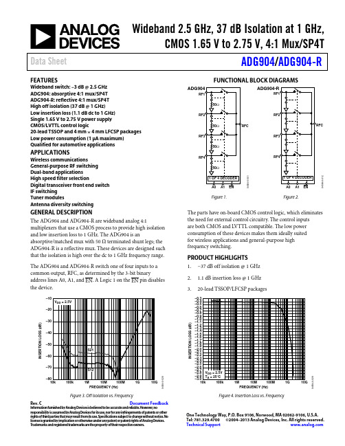
Figure 4. Insertion Loss vs. Frequency
One Technology Way, P.O. Box 9106, Norwood, MA 02062-9106, U.S.A. Tel: 781.329.4700 ©2004–2013 Analog Devices, Inc. All rights reserved. Technical Support
DOCUMENTATION
AN-952: ADG9xx Wideband CMOS Switches: Frequently Asked Questions CN-0211: IF Band-Pass Filter Bank Switching Network for Wireless Infrastructure Use Circuits from the Lab™ in Your Next Design CMOS Switches Offer High Performance in Low Power, Wideband Applications RF Source Booklet
04504-0-029
04504-0-012
IMPORTANT LINKS for the ADG904_904R*
Last content update 08/16/2013 12:48 pm
TI芯片总汇
OPA333AID OPA2333AID OPA335AID
OPA2335AID
OPA365AID
OPA2365AID
OPA727AIDGKT OPA2727AID OPA4727AIPW OPA734AID TLV2460IP TLV2462IP
TLV2463IN TLV2465IN
TPS40200D
TPS40211DGQ
TUSB3410IVF TMP275AID ISO7221MD ISO7220MD ISO7241MD ISO7240MD CC1101RTK CC2500RTK CC2480A1RTC CC2520RHDT CC2591RGVT
电压反馈高速放大
器
SAR 型 ADC
TL431BILP JFET 高速放大器 OPA656U OPA657U
THS4631D
流水线型 ADC
TPS74401KTWT TPS75901KTTT TPS70302PWP TPS54K/SWIFT TPS54160DGQ TPS5430DDA TPS5450DDA TPS54350PWP TPS54550PWP
精密对数放大器数
LOG112AID
电流基准 REF200AU
电流反馈放大器馈 压控增益放大器益
OPA684ID
VCA820ID
OPA2684ID
VCA822ID
OPA691ID
VCA810ID
OPA2691ID
OPA695ID
OPA2695ID
OPA694ID
THS3001ID THS3091D
音频功放
时钟发生和分配器
TPS54331D
电压反向器
MSP430F4793IPZ
- 1、下载文档前请自行甄别文档内容的完整性,平台不提供额外的编辑、内容补充、找答案等附加服务。
- 2、"仅部分预览"的文档,不可在线预览部分如存在完整性等问题,可反馈申请退款(可完整预览的文档不适用该条件!)。
- 3、如文档侵犯您的权益,请联系客服反馈,我们会尽快为您处理(人工客服工作时间:9:00-18:30)。
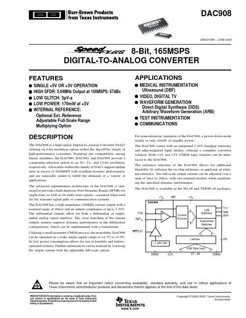
DESCRIPTION
The DAC904 is a high-speed, Digital-to-Analog Converter (DAC) offering a 14-bit resolution option within the family of highperformance converters. Featuring pin compatibility among family members, the DAC908, DAC900, and DAC902 provide a component selection option to an 8-, 10-, and 12-bit resolution, respectively. All models within this family of DACs support update rates in excess of 165MSPS with excellent dynamic performance, and are especially suited to fulfill the demands of a variety of applications.
The advanced segmentation architecture of the DAC904 is optimized to provide a high Spurious-Free Dynamic Range (SFDR) for single-tone, as well as for multi-tone signals— essential when used for the transmit signal path of communication systems.
The DAC904 is available in SO-28 and TSSOP-28 packages.
+VA DAC904
FSA REFIN
BW
+VD
Current Sources
LSB Switches
Segmented Switches
IOUT IOUT BYP
INT/EXT
+1.24V Ref.
q WAVEFORM GENERATION
Direct Digital Synthesis (DDS) Arbitrary Waveform Generation (ARB) q MEDICAL/ULTRASOUND q HIGH-SPEED INSTRUMENTATION AND CONTROL q VIDEO, DIGITAL TV
元器件交易网
DAC904
DAC904
DAC904
SBAS095C – MAY 2002
14-Bit, 165MSPS DIGITAL-TO-ANALOG CONVERTER
FEATURES
q SINGLE +5V OR +3V OPERATION q HIGH SFDR: 20MHz Output at 100MSPS: 64dBc q LOW GLITCH: 3pV-s q LOW POWER: 170mW at +5V q INTERNAL REFERENCE:
ESD damage can range from subtle performance degradation to complete device failure. Precision integrated circuits may be more susceptible to damage because very small parametric changes could cause the device not to meet its published specifications.
AGND
CLK
Latches
PD
14-Bit Data In that an important notice concerning availability, standard warranty, and use in critical applications of Texas Instruments semiconductor products and disclaimers thereto appears at the end of this data sheet.
The reference structure of the DAC904 allows for additional flexibility by utilizing the on-chip reference, or applying an external reference. The full-scale output current can be adjusted over a span of 2-20mA, with one external resistor, while maintaining the specified dynamic performance.
PRODUCTION DATA information is current as of publication date. Products conform to specifications per the terms of Texas Instruments standard warranty. Production processing does not necessarily include testing of all parameters.
Optional Ext. Reference Adjustable Full-Scale Range Multiplying Option
APPLICATIONS
q COMMUNICATION TRANSMIT CHANNELS WLL, Cellular Base Station Digital Microwave Links Cable Modems
Utilizing a small geometry CMOS process, the monolithic DAC904 can be operated on a wide, single-supply range of +2.7V to +5.5V. Its low power consumption allows for use in portable and
Copyright © 2002, Texas Instruments Incorporated
元器件交易网
ABSOLUTE MAXIMUM RATINGS
+VA to AGND ......................................................................... –0.3V to +6V +VD to DGND ........................................................................ –0.3V to +6V AGND to DGND ................................................................. –0.3V to +0.3V +VA to +VD ............................................................................... –6V to +6V CLK, PD to DGND ....................................................... –0.3V to VD + 0.3V D0-D13 to DGND ......................................................... –0.3V to VD + 0.3V IOUT, IOUT to AGND .......................................................... –1V to VA + 0.3V BW, BYP to AGND ....................................................... –0.3V to VA + 0.3V REFIN, FSA to AGND ................................................... –0.3V to VA + 0.3V INT/EXT to AGND ........................................................ –0.3V to VA + 0.3V Junction Temperature .................................................................... +150°C Case Temperature ......................................................................... +100°C Storage Temperature ..................................................................... +125°C
The DAC904 has a high impedance (200kOhm) current output with a nominal range of 20mA and an output compliance of up to 1.25V. The differential outputs allow for both a differential or single-ended analog signal interface. The close matching of the current outputs ensures superior dynamic performance in the differential configuration, which can be implemented with a transformer.