串口电平转换芯片数据手册SP3222_3232E
SP3222E_3232E_cn

4
3
C2+
反相电荷泵电容的正极。
5
5
4
C2-
反相电荷泵电容的负极。
6
6
5
V-
电荷泵产生的-5.5V 电压。
7
7
6
T1OUT RS-232 驱动器输出。
15
17
14
T2OUT RS-232 驱动器输出。
8
8
7
R1IN RS-232 接收器输入。
14
16
13
R2IN RS-232 接收器输入。
9
9
8
R1OUT TTL/CMOS 接收器输出。
20
-
为低电平时关闭驱动器(高阻输出)和片内电荷泵供电电
源。
N.C.
悬空。
-
11,14
-
图 4 SP3222E 管脚配置 5
广州周立功单片机发展有限公司 Tel:(020)38730976 38730977 Fax:38730925 http://
图 5 SP3222E 管脚配置
TXIN,EN………………………………………….………………………………………….……..-0.3V~+6.0V RXIN……………………………………………………………………………………………….……..±15V 输出电压 TXOUT………………………………………………………………………………………………….. ±15V
±15kV 人体放电模式 ±15kV IEC1000-4-2 气隙放电 ±8kV IEC1000-4-2 接触放电
描述
SP3222E/3232E 系列是 RS232 收发器对便携式或手持式应用如笔记本或掌上型电脑的一种解决方案。 SP3222E/3232E 系列有一个高效的电荷泵,工作电压为 3.3V 时只需 0.1µF 电容就可进行操作。电荷泵允许 SP3222E/3232E 系列在+3.3V 到+5.0V 内的某个电压下发送符合 RS-232 的信号。SP3222E/3232E 系列是一 个 2 驱动器/2 接收器的器件,适用于便携式或手持式设备(如笔记本或掌上型电脑)。SP3222E/3232E 器件 的 ESD 保护使得驱动器和接收器的管脚可承受±15kV 人体放电模式和 IEC1000-4-2 气隙放电模式。 SP3222E 器件包含一种低功耗关断模式,该模式下器件的驱动器输出和电荷泵被禁止。关断状态下,电源 电流低于 1µA。
TTL-RS232模块SP3232学习手册
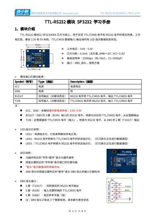
深圳市技新电子科技有限公司www.jixin.pro TTL-RS232SP3232EEN-L/TR V1.0.0.0 TTL-RS232模块SP3232学习手册1、模块介绍TTL-RS232模块以SP3232EEN芯片为核心,用于实现TTL/COMS电平和RS232电平的相互转换。
工作电压宽,兼容3.3V和5V系统。
TTL/CMOS数据输入/输出端均有LED指示数据收发状态。
工作电压:3.0V~5.5V芯片功耗:0.3mA(无负载,AMB=+25°,VCC=3.3V)最高波特率:235Kbps(RL=3kΩ,CL=1000pF)接口:DB9_母头,使用方便模块接口引脚功能表:Symbol(符号)Type(类型)Description(描述)VCC电源电源电压GND电源地R1OUT信号输出(对模块而言)RS232电平转TTL/CMOS电平,输出TTL/CMOS电平T1IN信号输入(对模块而言)TTL/CMOS电平转RS232电平,输入TTL/CMOS电平注:⏹VCC、GND:本模块需外部电源供电:3.0V~5.5V⏹R1OUT:DB9的3脚(R1IN)输入的RS232电平,转换为对应的TTL/CMOS电平,从此管脚输出⏹T1IN:此管脚接收TTL/CMOS电平(输入),转换为RS232电平,从DB9的2脚(T1OUT)输出 LED指示灯说明:⏹LED1:电源指示灯。
灯亮表明模块供电正常。
⏹LED2:RS232电平转换为TTL/CMOS电平的状态指示灯。
(灯闪表示正在进行数据通信)⏹LED3:TTL/CMOS电平转换为RS232电平的状态指示灯。
(灯闪表示正在进行数据通信)丝印说明:⏹元器件附近的“字符+数字”表示元器件编号⏹焊盘位置附近的“字符串”表示接口的引脚功能⏹“箭头”表示数据流的传输方向⏹DB9母头的焊盘位置附近的“数字”表示DB9母头的接口引脚标号DB9母头接口:⏹2脚(T1OUT):将转换后的RS232电平输出⏹3脚(R1IN):输入将要转换的TTL/CMOS电平⏹5脚(GND):电压参考平面(地)⏹注:DB9母头只有这3个管脚有用,其余都为悬空状态深圳市技新电子科技有限公司www.jixin.pro TTL-RS232SP3232EEN-L/TR V1.0.0.0 焊盘C6、C7的作用:⏹C6并联在T1OUT(DB9母头的2脚)和地之间、C7并联在R1IN(DB9母头的3脚)和地之间。
sp3232中文资料说明书

输出漏电流 低输出电压 高输出电压 驱动器输出 输出电压范围
±0.05 VCC-0.6 VCC-0.1
±10 0.4
±5.0
±5.4
输出电阻
300
输出短路电流
±35
±60
±70
±100
输出漏电流
±25
接收器输入
输入电压范围
-15
+15
输入低阈值
0.6
1.2
0.8
1.5
输入高阈值
1.5
2.4
1.8
2.4
1
RXOUT……………………………………………………………………..………………-0.3V~(VCC+0.3V) 短路期间 TXOUT……………………………………………………………………………...………………………不变 存储器温度………………………………………………………………………………………-65℃~+150℃ 每种封装的功耗 20-脚 SSOP ………………………………………………………………………………….………………………..750mW (大于+70℃时以 9.25mW/℃降低) 18-脚 PDIP ………………………………………………………………………….……………………………..1220mW (大于+70℃时以15.2mW/℃降低) 18-脚 SOIC …………………………………………………………………………….…………………………..1260mW (大于+70℃时以 15.7mW/℃降低) 20-脚 TSSOP ………………………………………………………………………………….………………………..890mW (大于+70℃时以 11.1mW/℃降低) 16-脚 SSOP ………………………………………………………………………………….………………………..775mW (大于+70℃时以 9.69mW/℃降低) 16-脚 PDIP ………………………………………………………………………………….………………………1150mW (大于+70℃时以14.3mW/℃降低) 16-脚 宽SOIC ………………………………………………………………………………….………………………..900mW (大于+70℃时以 11.2mW/℃降低) 16-脚 TSSOP ………………………………………………………………………………….………………………..850mW (大于+70℃时以 10.5mW/℃降低) 20-脚 nSOIC ………………………………………………………………………………….……………………..1086mW (大于+70℃时以 13.57mW/℃降低)
3232E中文资料
3232E中文资料Anasys Semiconductor, Inc.High ESD-Protected, Low Power, 3.0V to 5.5V ,Single Supply RS-232 TransceiversMAX3222E/3232EGeneral DescriptionApplicationsFeaturesNotebook, Sub notebook, and Palmtop Computers Battery-Powered / Hand-Held Equipment POS terminal / Intelligent Network Switch DMM / Printers Smart Phones xDSL Modems The MAX3222E/MAX3232E are 2 driver, 2 receiver RS-232 transceiver solutions intended for portable or hand-held applications, features low power consumption, high data-rate capabilities, and enhanced ESD protection. The ESD tolerance of the MAX3222E/3232E devices is over ±15kV for both human body model and IEC1000-4-2 air discharge test methods.A low-dropout transmitter output stage delivers true RS-232 performance from a +3.0V to +5.5V power supply, using an internal dual charge pump. The charge pump requires only four small 0.1μF capacitors for operation from a +3.3V supply. Each device guarantees operation at data rates of 250kbps while maintaining RS-232 output levels.The MAX3222E features a 1μA shutdown mode that reduces power consumption in battery-powered portable systems. The MAX3222E receivers remain active in shutdown mode, allowing monitoring o f external devices while consuming only 1μA of supply current. The MAX3222E and MAX3232E are pin, package, and functionally compatible with the industry-standard MAX242and MAX232, respectively.Meets true EIA/TIA-232-F Standards from a +3.0V to +5.5V power supply Interoperable with EIA/TIA - 232 and adheres to EIA/TIA - 562 1μA Low-Power Shutdown (MAX3222E) Enhanced ESD Specifications:15kV Human Body Model 15kV IEC1000-4-2 Air Discharge 8kV IEC1000-4-2 Contact Discharge 250 kbps Minimum Transmission RateIdeal for Handheld, Battery Operated Applications Latch up FreeGuaranteed 30V/μs Max Slew Rate BiCMOS TechnologyOrdering InformationAbsolute Maximum RatingsStresses beyond those listed under Absolute Maximum Ratings may cause permanent damage to the device. These are stress ratings only, and functional operation of the device at these or any other conditions beyond those indicated in the operational sections of the specifications is not implied. Exposure to absolute maximum rating conditions for extended periods may affect device reliability.Pin DescriptionElectrical Characteristics(VCC = +3V to +5.5V, C1-C4 = 0.1μF, T A = T MIN to T MAX, unless otherwise noted. Typical values are at T A = +25°C.)Typical Operating CharacteristicsAnasys Semiconductor, Inc.(VCC = +3.3V, 250kbps data rate, 0.1μF capacitors, all transmitters loaded with 3k ? and CL, TA = +25°C, unless otherwise noted.)T1 TRANSMITTING AT 250kbps T2 TRANSMITTING AT 15.6kbpsTypical Operating CircuitsC 3C 4Detailed DescriptionAnasys Semiconductor, Inc.Dual Charge-Pump Voltage ConverterThe MAX3222E/MAX3232Es’ internal power supply consists of a regulated dual charge pump that provides output voltages of +5.5V (doubling charge pump) and -5.5V (inverting charge pump) over the +3.0V to +5.5V VCC range. The charge pump operates in discontinuous mode; if the output voltages are less than 5.5V, the charge pump is enabled, and if the outputvoltages exceed 5.5V, the charge pump is disabled. Each charge pump requires a flying capacitor (C1, C2) and a storage capacitor (C3, C4) to generate the V+ and V- supplies. RS-232 Transmitters The transmitters are inverting level translators that convert TTL/CMOS-logic levels to ±5V EIA/TIA-232 compliant levels. The MAX3222E/MAX3232E transmitters guarantee a 250kbps data rate with worst-case loads of 3K Ω parallel with 1000pF. Transmitters can be paralleled to drive multiple receivers. The MAX3222E transmitters are disabled and the outputs are forced into ahigh-impedance state when the device is in shutdown mode (SHDN =GND). The MAX3222E/MAX3232E permits the outputs to be driven up to ±12V in shutdown. RS-232 ReceiversThe receivers convert RS-232 signals to CMOS-logic output levels. The MAX3222E receivers have inverting three-state outputs. Drive EN high to place the receiver(s) into a high impedance state. Receivers can be either active or inactive in shutdown. MAX3222ESupply current falls to less than 1μA in shutdown mode (= GND). When shutdown, the device’s charge pumps are shut off, V+ is pulled down to VCC, V- is pulled to ground, and the transmitter outputs are disabled (high impedance). The time required to recov er from shutdown is typically 100μs. Connect SHDN to VCC if shutdown mode is not used. ±15kV ESD ProtectionESD-protection structures are incorporated to protect against electrostatic discharges encountered during handling and assembly. The driver outputs and receiver inputs of the MAX3222E/MAX3232E have extra protection against staticelectricity. The ESD structures withstand high ESD in all states:normal operation, shutdown, and powered down. After an ESD event, Circuits keep working without latch up. ESD protection can be tested in various ways; the transmitter outputs and receiver inputs for the MAX3222E/MAX3232E are characterized for protection to the following limits: ? ±15kV using the Human Body Model±8kV using the Contact Discharge method specified in IEC 1000-4-2 ? ±15kV using the Air-Gap Discharge method specified in IEC 1000-4-2Anasys Semiconductor, Inc.Application InformationCapacitor SelectionThe capacitor type used for C1–C4 is not critical for proper operation; polarized or non-polarized capacitors can be used. The charge pump requires 0.1μF capacitors for 3.3V operation. Increasing the capacitor values (e.g., by a factor of 2) reduces ripple on the transmitter outputs and slightly reduces power consumption. C2, C3, and C4 can be increased without changing C1’s value. When using the minimum required capacitor values, make sure the capacitor value does not degrade excessively with temperature. If in doubt, use capacitors with a larger nominal value. The capacitor’s equivalent series resistanc e (ESR), which usually rises at low temperatures, influences the amount of ripple on V+ and V- output voltages.Power-Supply DecouplingIn most circumstances, a 0.1μF VCC bypass capacitor is adequate. In applications sensitive to power-supply noise, use a capacitor of the same value as charge pump capacitor C1. Connect bypass capacitors as close to the IC as possible.Operation Down to 2.7VTransmitter outputs meet EIA/TIA-562 levels of ±3.7V with supply voltages as low as 2.7V. Transmitter Outputs Recovering from ShutdownWhen MAX3222E’s two transmitter outputs were recovering from shutdown mode, the two transmitter outputs are shown going to opposite RS-232 levels (one transmitter input is high; the other is low) as they become active. Each transmitter is loaded with 3K resistor in parallel with 2500pF. The transmitter outputs display no ringing or undesirable transients as they come out of shutdown. Note that the transmitters are enabled only when the magnitude of V- exceeds approximately -3.0V. Interconnection with 3V and 5V LogicThe MAX3222E/MAX3232E can directly interface with various 3V and 5V logic families, including ACT and HCT CMOS.。
sp3232中文资料_数据手册_参数

V
IOUT = 1.6mA
V
IOUT = -1.0mA
V All driver outputs loaded with 3kΩ to GND, TAMB = +25oC
Exar Corporation 48720 Kato Road, Fremont CA, 94538 • 510-668-7017 •
PARAMETER DC CHARACTERISTICS Supply Current
MIN.Supply Current
1.0
LOGIC INPUTS AND RECEIVER OUTPUTS Input Logic Threshold LOW
MAX. UNITS CONDITIONS
DESCRIPTION The SP3222E/SP3232E series is an RS-232 transceiver solution intended for portable or hand-held applications such as notebook or palmtop computers. The SP3222E/SP3232E series has a high-efficiency, charge-pump power supply that requires only 0.1µF capaci-
SP3222E/SP3232E_101_031413
These are stress ratings only and functional operation of the device at these ratings or any other above those indicated in the operation sections of the specifications below is not implied. Exposure to absolute maximum rating conditions for extended periods of time may affect reliability and cause permanent damage to the device.
RS-232收发器接口芯片SP3223E/3243E的原理及应用解读

RS-232收发器接口芯片SP3223E/3243E的原理及应用摘要:SP3223E/3243E是SIPEX公司生产的RS-232收发器接口芯片。
该器件内部含有一个高效电荷泵,可在单+3.0V~+5.5V电源下产生±5.5V的RS-232电平,并支持EIA/TIA-232和ITU-TV.28/V.24通信协议,因而可用于笔记本电脑等便携式设备。
文章分析了SP3223E/3243E的结构原理和主要特点,给出了它的典型应用电路。
关键词:电荷泵;自动上线;驱动器;收发器1概述SP3223E/3243E是SIPEX公司生产的RS-232收发器,它支持EIA/TIA-232和ITU-TV.28/V.24通信协议,适用于便携式设备使用(如笔记本电脑及PDA)。
SP3223E/3243E内有一个高效电荷泵,可在单+3.0V~+5.5V电源下产生±5.5V的RS-232电平,该技术已申请了美国专利(专利号为U.S.--5 306 954)。
满负载时,SP3223E/3243E器件可工作于235kbps的数据传输率。
3.3V时仅需0.1μF的电容。
SP3223E是一个双驱动器/双接收器芯片,SP3243E则是一个三驱动器/五接收器芯片,是笔记本电脑或PDA的理想器件。
SP3243E包含一个总是处于激活状态的补充接收器,可在关断状态下监控外设(如调制解调器)。
由于具有自动上线特性,因此,当其与一个相关外设之间接上RS-232电缆并处于工作状态下时,设备会自动醒来。
否则,如果电流不足1mA,设备会自动关断。
SP3243E包含一个补充接收器,当电源断开时,该接收器可保护UART或串行控制器芯片。
SP3223E和SP3243E是敏感电源设计的理想选择。
SP3223E和SP3243E的自动上线电路减少了电源电流降到1mA以下的可能性。
在大多数便携式应用场合,RS-232电缆可被断开或是将外设关闭。
在上述情况下,其内部的电荷泵和驱动器也会被关闭。
MAX3222EEUP中文资料
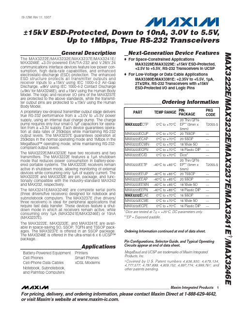
Battery-Powered Equipment Cell Phones Cell-Phone Data Cables Notebook, Subnotebook, and Palmtop Computers
Applications
Printers Smart Phones xDSL Modems
_______________Ordering Information
PART
TEMP RANGE
PINPACKAGE
PKG CODE
MAX3222ECTP MAX3222ECUP
0°C to +70°C 0°C to +70°C
20 Thin QFNEP** (5mm x 5mm) 20 TSSOP
♦ For Low-Voltage or Data Cable Applications MAX3380E/MAX3381E: +2.35V to +5.5V, 1µA, 2Tx/2Rx, RS-232 Transceivers with ±15kV ESD-Protected I/O and Logic Pins
MAX3222EEPN -40°C to +85°C 18 Plastic DIP —
MAX3232ECAE 0°C to +70°C 16 SSOP
—
MAX3232ECWE 0°C to +70°C 16 Wide SO —
MAX3232ECPE 0°C to +70°C 16 Plastic DIP —
A proprietary low-dropout transmitter output stage delivers true RS-232 performance from a +3.0V to +5.5V power supply, using an internal dual charge pump. The charge pump requires only four small 0.1µF capacitors for operation from a +3.3V supply. Each device guarantees operation at data rates of 250kbps while maintaining RS-232 output levels. The MAX3237E guarantees operation at 250kbps in the normal operating mode and 1Mbps in the MegaBaud™ operating mode, while maintaining RS-232compliant output levels.
MAX3232电平转换原理图

MAX3232电平转换原理图
RS232TO TTL 通讯模块
实现RS232到TTL数据转换。
芯片采用MAX3232适用电压3V-5.5V,具有ESD保护功能、支持流控制、零延时自动收发转换和波特率自适应特点,即插即用,稳定可靠。
主要资源:
一、DB9母头RS232接口带流控功能可直接接电脑
二、2.54排针RS232接口带流控功能可替代DB9接头
三、3个指示灯分别是电源指示灯、数据收指示灯、数据发指示灯
四、2.54排针TTL接口带流控功能可直接接TTL设备
淘宝网站
https:///?spm=2013.1.1000126.d 21.lOnOC1
以MCU单片机TTL到PC台式机RS232数据通信为例
1、PC台式机接DB9接口
2、MCU通过杜邦线接排针P1接口
P1接口说明
1GND接GND信号流向:GND
2VCC接3V-5V信号流向:VCC<--MCU_5V/MCU_3.3V
3RX接MCU_TX信号流向:PC_RX<--MAX3232<--RX
4TX接MCU_RX信号流向:PC_TX-->MAX3232-->TX
5CTS接MCU_RTS信号流向:PC_CTS<--MAX3232<--MCU_RTS 6RTS接MCU_CTS信号流向:PC_RTS-->MAX3232-->MCU_CTS
产品附件
1、RS232-TTL小板一个
2、杜邦线十根十种颜色
3、防静电自封袋一个
4、原理图
淘宝
https:///?spm=2013.1.1000126.d 21.lOnOC1产品图片。
- 1、下载文档前请自行甄别文档内容的完整性,平台不提供额外的编辑、内容补充、找答案等附加服务。
- 2、"仅部分预览"的文档,不可在线预览部分如存在完整性等问题,可反馈申请退款(可完整预览的文档不适用该条件!)。
- 3、如文档侵犯您的权益,请联系客服反馈,我们会尽快为您处理(人工客服工作时间:9:00-18:30)。
DESCRIPTIONs Meets true EIA/TIA-232-F Standards from a +3.0V to +5.5V power supplys 235KBps Transmission Rate Under Load s 1µA Low-Power Shutdown with Receivers Active (SP3222E )s Interoperable with RS-232 down to +2.7V power sources Enhanced ESD Specifications: ±15kV Human Body Model±15kV IEC1000-4-2 Air Discharge ±8kV IEC1000-4-2 Contact DischargeThe SP3222E/3232E series is an RS-232 transceiver solution intended for portable or hand-held applications such as notebook or palmtop computers. The SP3222E/3232E series has a high-efficiency, charge-pump power supply that requires only 0.1µF capacitors in 3.3V operation. This charge pump allows the SP3222E/3232E series to deliver true RS-232performance from a single power supply ranging from +3.3V to +5.0V. The SP3222E/3232E are 2-driver/2-receiver devices. This series is ideal for portable or hand-held applications such as notebook or palmtop computers. The ESD tolerance of the SP3222E/3232E devices are over ±15kV for both Human Body Model and IEC1000-4-2 Air discharge test methods. The SP3222E device has a low-power shutdown mode where the devices' driver outputs and charge pumps are disabled. During shutdown, the supply current falls to less than 1µA.SELECTION TABLEL E D O M s e i l p p u S r e w o P 232-S R s r D e v i r 232-S R sr e v i e c e R l a n r e t x E st n e n o p m o C nw o d t u h S L T T a S -3e t t f o .o N s n i P 2223P S V 5.5+o t V 0.3+224s e Y s e Y 02,812323P S V5.5+o t V 0.3+224oN oN 61RE T E M A R A P .N I M .P Y T .X A M ST I N U SN O I T I D N O C S C I T S I R E T C A R A H C C D tn e r r u C y l p p u S 3.00.1A m T ,d a o l o n B M A 52+=o V ,C C C V 3.3=tn e r r u C y l p p u S n w o d t u h S 0.101µA,D N G =N D H S T B M A 52+=o V ,C C C V3.3+=S T U P T U O R E V I E C E R D N A S T U P N I C I G O L W O L d l o h s e r h T c i g o L t u p n I 8.0V 2e t o N ,N D H S ,N E ,N I x T H G I H d l o h s e r h T c i g o L t u p n I 0.24.2V V C C 2e t o N ,V 3.3=V C C 2e t o N ,V 0.5=t n e r r u C e g a k a e L t u p n I 10.0±0.1±µA ,N D H S ,N E ,N I x T T B M A 52+=o C t n e r r u C e g a k a e L t u p t u O 50.0±01±µA d e l b a s i d s r e v i e c e r W O L e g a t l o V t u p t u O 4.0V I T U O A m 6.1=H G I H e g a t l o V t u p t u O V C C 6.0-V C C 1.0-VI T U O Am 0.1-=S T U P T U O R E V I R D gn i w S e g a t l o V t u p t u O 0.5±4.5±Vk 3Ω,s t u p t u o r e v i r d l l a t a d n u o r g o t d a o l T B M A 52+=o Cec n a t s i s e R t u p t u O 003ΩV C C T ,V 0=-V =+V =T U O =+V 2t n e r r u C t i u c r i C -t r o h S t u p t u O 53±07±06±001±A m A m V T U O V 0=V T U O =+V51tn e r r u C e g a k a e L t u p t u O 52±µAV T U O =+V ,V 21C C de l b a s i d s r e v i r d ,V 5.5o t V 0=NOTE 1: V+ and V- can have maximum magnitudes of 7V, but their absolute difference cannot exceed 13V.ABSOLUTE MAXIMUM RATINGSThese are stress ratings only and functional operation of the device at these ratings or any other above those indicated in the operation sections of the specifications below is not implied. Exposure to absolute maximum rating conditions for extended periods of time may affect reliability and cause permanent damage to the device.V CC ................................................................-0.3V to +6.0V V+ (NOTE 1)................................................-0.3V to +7.0V V- (NOTE 1)................................................+0.3V to -7.0V V+ + |V-| (NOTE 1)....................................................+13V I CC (DC V CC or GND current).................................±100mAInput VoltagesTxIN, EN .....................................................-0.3V to +6.0V RxIN.............................................................................±25V Output VoltagesTxOUT.....................................................................±13.2V RxOUT..............................................-0.3V to (V CC + 0.3V)Short-Circuit DurationTxOUT...............................................................Continuous Storage Temperature.................................-65°C to +150°C Power Dissipation Per Package20-pin SSOP (derate 9.25mW/o C above +70o C).....750mW 18-pin PDIP (derate 15.2mW/o C above +70o C)....1220mW 18-pin SOIC (derate 15.7mW/o C above +70o C)...1260mW 20-pin TSSOP (derate 11.1mW/o C above +70o C)..890mW 16-pin SSOP (derate 9.69mW/o C above +70o C).....775mW 16-pin PDIP (derate 14.3mW/o C above +70o C)....1150mW 16-pin Wide SOIC (derate 11.2mW/o C above +70o C)900mW 16-pin TSSOP (derate 10.5mW/o C above +70o C)..850mW 16-pin nSOIC (derate 13.57mW/°C above +70°C)..1086mWSPECIFICATIONSUnless otherwise noted, the following specifications apply for V CC = +3.0V to +5.0V with T AMB = T MIN to T MAXR E T E M A R A P .N I M .P Y T .X A M ST I N U SN O I T I D N O C S T U P N I R E V I E C E R e g n a R e g a t l o V t u p n I 51-51+V W O L d l o h s e r h T t u p n I 6.08.02.15.1V V C C V 3.3=V C C V 0.5=H G I H d l o h s e r h T t u p n I 5.18.14.24.2V V C C V 3.3=V C C V0.5=s i s e r e t s y H t u p n I 3.0V ec n a t s i s e R t u p n I 357k ΩS C I T S I R E T C A R A H C G N I M I T e t a R a t a D m u m i x a M 021532s p b k R L k 3=ΩC ,L g n i h c t i w s r e v i r d e n o ,F p 0001=y a l e D n o i t a g a p o r P r e v i r D 0.10.1µs µs t L H P R ,L K 3=ΩC ,L F p 0001=t H L P R ,L K 3=ΩC ,L F p 0001=y a l e D n o i t a g a p o r P r e v i e c e R 3.03.0µs t L H P C ,T U O x R o t N I x R ,L F p 051=t H L P C ,T U O x R o t N I x R ,L Fp 051=e m i T e l b a n E t u p t u O r e v i e c e R 002s n e m i T e l b a s i D t u p t u O r e v i e c e R 002s n w e k S r e v i r D 001005s n t |L H P t -H L P T ,|B M A 52=o C we k S r e v i e c e R 0020001s n t |L H P t -H L P |et a R w e l S n o i g e R -n o i t i s n a r T 03/V µsV C C R ,V 3.3=L K 3=ΩT ,B M A 52=o ,C V 0.3+o t V 0.3-m o r f n e k a t s t n e m e r u s a e m V0.3-o t V 0.3+r o SPECIFICATIONS (continued)Unless otherwise noted, the following specifications apply for V CC = +3.0V to +5.0V with T AMB = T MIN to T MAX .Typical Values apply at V CC = +3.3V or +5.0V and T AMB = 25o C.NOTE 2: Driver input hysteresis is typically 250mV.Capacitance for the SP3222 and the SP3232SP3222 and the SP3232Transmitting Data for the SP3222 and the SP3232TYPICAL PERFORMANCE CHARACTERISTICSUnless otherwise noted, the following performance characteristics apply for V CC = +3.3V, 235kbps data rates, all drivers loaded with 3k Ω, 0.1µF charge pump capacitors, and T AMB = +25°C.DESCRIPTIONThe SP3222E/3232E transceivers meet the EIA/TIA-232 and V.28/V.24 communication proto-cols and can be implemented in battery-pow-ered, portable, or hand-held applications such as notebook or palmtop computers. The SP3222E/3232E devices all feature Sipex's proprietary on-board charge pump circuitry that generates 2x V CC for RS-232 voltage levels from a single +3.0V to +5.5V power supply. This series is ideal for +3.3V-only systems, mixed +3.3V to +5.5V systems, or +5.0V-only systems that re-quire true RS-232 performance. The SP3222E/3232E series have drivers that operate at a typi-cal data rate of 235Kbps fully loaded.The SP3222E and SP3232E are 2-driver/2-re-ceiver devices ideal for portable or hand-held applications. The SP3222E features a 1µA shutdown mode that reduces power consump-tion and extends battery life in portable systems.Its receivers remain active in shutdown mode,allowing external devices such as modems to be monitored using only 1µA supply current.THEORY OF OPERATIONThe SP3222E/3232E series are made up of three basic circuit blocks: 1. Drivers, 2. Receivers,and 3. the Sipex proprietary charge pump.DriversThe drivers are inverting level transmitters that convert TTL or CMOS logic levels to ±5.0V EIA/TIA-232 levels inverted relative to the in-put logic levels. Typically, the RS-232 output voltage swing is ±5.5V with no load and at least ±5V minimum fully loaded. The driver outputs are protected against infinite short-circuits to ground without degradation in reliability. Driver outputs will meet EIA/TIA-562 levels of ±3.7V with supply voltages as low as 2.7V.The drivers typically can operate at a data rate of 235Kbps. The drivers can guarantee a data rate of 120Kbps fully loaded with 3K Ω in parallel with 1000pF, ensuring compatibility with PC-to-PC communication software.The slew rate of the driver output is internally limited to a maximum of 30V/µs in order to meet the EIA standards (EIA RS-232D 2.1.7, Para-graph 5). The transition of the loaded output from HIGH to LOW also meets the monotonic-ity requirements of the standard.The SP3222E/3232E drivers can maintain high data rates up to 240Kbps fully loaded. Figure 8shows a loopback test circuit used to test the RS-232 drivers. Figure 9 shows the test results of the loopback circuit with all drivers active at 120Kbps with RS-232 loads in parallel with 1000pF capacitors. Figure 10 shows the test results where one driver was active at 235Kbps and all drivers loaded with an RS-232 receiver in parallel with a 1000pF capacitor. A solid RS-232 data transmission rate of 120Kbps provides compatibility with many designs in personal computer peripherals and LAN applications.The SP3222E driver's output stages are turned off (tri-state) when the device is in shutdown mode. When the power is off, the SP3222E device permits the outputs to be driven up to ±12V. The driver's inputs do not have pull-up resistors. Designers should connect unused inputs to V CC or GND.In the shutdown mode, the supply current falls to less than 1µA, where SHDN = LOW. When the SP3222E device is shut down, the device's driver outputs are disabled (tri-stated) and the charge pumps are turned off with V+ pulled down to V CC and V- pulled to GND. The time required to exit shutdown is typically 100µs.Connect SHDN to V CC if the shutdown mode is not used. SHDN has no effect on RxOUT or RxOUTB. As they become active, the two driver outputs go to opposite RS-232 levels where one driver input is HIGH and the other LOW. Note that the drivers are enabled only when the magnitude of V- exceeds approximately 3V.ReceiversThe receivers convert EIA/TIA-232 levels to TTL or CMOS logic output levels. All receivers have an inverting tri-state output. These receiver outputs (RxOUT) are tri-stated when the enable control EN = HIGH. In the shutdown mode, the receivers can be active or inactive. EN has no effect on TxOUT. The truth table logic of the SP3222E/3232E driver and receiver outputs can be found in Table 2.Since receiver input is usually from a transmis-sion line where long cable lengths and system interference can degrade the signal, the inputs have a typical hysteresis margin of 300mV. This ensures that the receiver is virtually immune to noisy transmission lines. Should an input be left unconnected, a 5k Ω pulldown resistor to ground will commit the output of the receiver to a HIGH state.Charge PumpThe charge pump is a Sipex –patented design (5,306,954) and uses a unique approach com-pared to older less–efficient designs. The charge pump still requires four external capacitors, but uses a four–phase voltage shifting technique to attain symmetrical 5.5V power supplies. The internal power supply consists of a regulated dual charge pump that provides output voltages 5.5V regardless of the input voltage (V CC ) over the +3.0V to +5.5V range.In most circumstances, decoupling the power supply can be achieved adequately using a 0.1µF bypass capacitor at C5 (refer to Figures 6 and 7).In applications that are sensitive to power-sup-ply noise, decouple V CC to ground with a capaci-tor of the same value as charge-pump capacitor C1. Physically connect bypass capacitors as close to the IC as possible.The charge pumps operate in a discontinuous mode using an internal oscillator. If the output voltages are less than a magnitude of 5.5V, the charge pumps are enabled. If the output voltage exceed a magnitude of 5.5V, the charge pumps are disabled. This oscillator controls the four phases of the voltage shifting. A description of each phase follows.Phase 1— V SS charge storage — During this phase of the clock cycle, the positive side of capacitors C 1and C 2 are initially charged to V CC . C l + is then switched to GND and the charge in C 1– is trans-ferred to C 2–. Since C 2+ is connected to V CC , the voltage potential across capacitor C 2 is now 2times V CC .Phase 2— V SS transfer — Phase two of the clock con-nects the negative terminal of C 2 to the V SS storage capacitor and the positive terminal of C 2to GND. This transfers a negative generated voltage to C 3. This generated voltage is regu-lated to a minimum voltage of -5.5V. Simulta-neous with the transfer of the voltage to C 3, the positive side of capacitor C 1 is switched to V CC and the negative side is connected to GND.Phase 3— V DD charge storage — The third phase of the clock is identical to the first phase — the charge transferred in C 1 produces –V CC in the negative terminal of C 1, which is applied to the negative side of capacitor C 2. Since C 2+ is at V CC , the voltage potential across C 2 is 2 times V CC .Table 2. Truth Table Logic for Shutdown and Enable ControlN D H S N E T U O x T T U O x R 00e t a t s -i r T e v i t c A 01e t a t s -i r T e t a t s -i r T 10e v i t c A e v i t c A 11ev i t c A et a t s -i r TPhase 4— V DD transfer — The fourth phase of the clock connects the negative terminal of C 2 to GND,and transfers this positive generated voltage across C 2 to C 4, the V DD storage capacitor. This voltage is regulated to +5.5V. At this voltage,the internal oscillator is disabled. Simultaneous with the transfer of the voltage to C 4, the positive side of capacitor C 1 is switched to V CC and the negative side is connected to GND, allowing the charge pump cycle to begin again. The charge pump cycle will continue as long as the opera-tional conditions for the internal oscillator are present.Since both V + and V – are separately generated from V CC ; in a no–load condition V + and V – will be symmetrical. Older charge pump approaches that generate V – from V + will show a decrease in the magnitude of V – compared to V + due to the inherent inefficiencies in the design.The clock rate for the charge pump typically operates at 250kHz. The external capacitors can be as low as 0.1µF with a 16V breakdown voltage rating.ESD ToleranceThe SP3222E/3232E series incorporates ruggedized ESD cells on all driver output and receiver input pins. The ESD structure is improved over our previous family for more rugged applications and environments sensitive to electro-static discharges and associated transients. The improved ESD tolerance is at least ±15kV without damage nor latch-up.There are different methods of ESD testing applied:a) MIL-STD-883, Method 3015.7b) IEC1000-4-2 Air-Discharge c) IEC1000-4-2 Direct Contact The Human Body Model has been the generally accepted ESD testing method for semiconduc-tors. This method is also specified in MIL-STD-883, Method 3015.7 for ESD testing. The premise of this ESD test is to simulate the human body’spotential to store electro-static energy and discharge it to an integrated circuit. The simulation is performed by using a test model as shown in Figure 17. This method will test the IC’s capability to withstand an ESD transient during normal handling such as in manufacturing areas where the ICs tend to be handled frequently.The IEC-1000-4-2, formerly IEC801-2, is generally used for testing ESD on equipment and systems. For system manufacturers, they must guarantee a certain amount of ESD protection since the system itself is exposed to the outside environment and human presence.The premise with IEC1000-4-2 is that the system is required to withstand an amount of static electricity when ESD is applied to points and surfaces of the equipment that are accessible to personnel during normal usage.The transceiver IC receives most of the ESD current when the ESD source is applied to the connector pins. The test circuit for IEC1000-4-2is shown on Figure 18. There are two methods within IEC1000-4-2, the Air Discharge method and the Contact Discharge method.With the Air Discharge Method, an ESD voltage is applied to the equipment under test (EUT) through air. This simulates an electrically charged person ready to connect a cable onto the rear of the system only to find an unpleasant zap just before the person touches the back panel. The high energy potential on the person discharges through an arcing path to the rear panel of the system before he or she even touches the system. This energy, whether discharged directly or through air, is predominantly a function of the discharge current rather than the discharge voltage.Variables with an air discharge such as approach speed of the object carrying the ESD potential to the system and humidity will tend to change the discharge current. For example, the rise time of the discharge current varies with the approach speed.Figure 14. Charge Pump WaveformsThe Contact Discharge Method applies the ESD current directly to the EUT. This method was devised to reduce the unpredictability of the ESD arc. The discharge current rise time is constant since the energy is directly transferred without the air-gap arc. In situations such as hand held systems, the ESD charge can be directly discharged to the equipment from a person already holding the equipment. The current is transferred on to the keypad or the serial port of the equipment directly and then travels through the PCB and finally to the IC.The circuit models in Figures 17 and 18 represent the typical ESD testing circuits used for all three methods. The C S is initially charged with the DC power supply when the first switch (SW1) is on. Now that the capacitor is charged, the second switch (SW2) is on while SW1 switches off. The voltage stored in the capacitor is then applied through R S, the current limiting resistor, onto the device under test (DUT). In ESD tests, the SW2 switch is pulsed so that the device under test receives a duration of voltage.Figure 17. ESD Test Circuit for Human Body ModelFigure 18. ESD Test Circuit for IEC1000-4-2Figure 19. ESD Test Waveform for IEC1000-4-230AI ¥0A15At=30nst ¥t=0nsFor the Human Body Model, the current limiting resistor (R S ) and the source capacitor (C S ) are 1.5k Ω an 100pF, respectively. For IEC-1000-4-2, the current limiting resistor (R S )and the source capacitor (C S ) are 330Ω an 150pF,respectively.The higher C S value and lower R S value in the IEC1000-4-2 model are more stringent than the Human Body Model. The larger storage capacitor injects a higher voltage to the test point when SW2 is switched on. The lower current limiting resistor increases the current charge onto the test point.Device Pin Human Body IEC1000-4-2Tested Model Air Discharge Direct Contact LevelDriver Outputs ±15kV ±15kV ±8kV 4Receiver Inputs ±15kV±15kV±8kV4Table 3. Transceiver ESD Tolerance LevelsPACKAGE:PLASTIC SHRINKPACKAGE:PLASTICDUAL–IN–LINE (NARROW)PACKAGE:PLASTICPACKAGE:PLASTICSMALL OUTLINE (SOIC)(NARROW)DIMENSIONSin inches (mm) Minimum/Maximum Symbol16 Lead20 Lead D0.193/0.2010.252/0.260(4.90/5.10)(6.40/6.60)e0.026 BSC0.026 BSC(0.65 BSC)(0.65 BSC)PACKAGE:PLASTIC THINSMALL OUTLINE(TSSOP)ORDERING INFORMATIONModel Temperature Range Package Type SP3222ECA.............................................0˚C to +70˚C..........................................20-Pin SSOP SP3222ECP.............................................0˚C to +70˚C............................................18-Pin PDIP SP3222ECT.............................................0˚C to +70˚C...........................................18-Pin SOIC SP3222ECY.............................................0˚C to +70˚C........................................20-Pin TSSOP SP3222EEA............................................-40˚C to +85˚C........................................20-Pin SSOP SP3222EEP............................................-40˚C to +85˚C..........................................18-Pin PDIP SP3222EET............................................-40˚C to +85˚C.........................................18-Pin SOIC SP3222EEY............................................-40˚C to +85˚C......................................20-Pin TSSOP SP3232ECA.............................................0˚C to +70˚C..........................................16-Pin SSOP SP3232ECP.............................................0˚C to +70˚C............................................16-Pin PDIP SP3232ECT.............................................0˚C to +70˚C..................................16-Pin Wide SOIC SP3232ECN.............................................0˚C to +70˚C.........................................16-Pin nSOIC SP3232ECY.............................................0˚C to +70˚C........................................16-Pin TSSOP SP3232EEA............................................-40˚C to +85˚C........................................16-Pin SSOP SP3232EEP............................................-40˚C to +85˚C..........................................16-Pin PDIP SP3232EET............................................-40˚C to +85˚C................................16-Pin Wide SOIC SP3232EEN............................................-40˚C to +85˚C.......................................16-Pin nSOIC SP3232EEY............................................-40˚C to +85˚C......................................16-Pin TSSOP。