16位模拟多路复用器CD4067B
CD74HC4067SM96中文资料

Copyright © 2003, Texas Instruments Incorporated
1
元器件交易网
Functional Diagram
10 S0 11 S1 14 S2
13 S3
CD74HC4067, CD74HCT4067
I0 9
PN
BINARY 1 OF 16 DECODER SN = 5 STAGES E = 4 STAGES
Thermal Information
Thermal Resistance (Typical)
θJA (oC/W)
E (PDIP) Package, Note 1 . . . . . . . . . . . . . . . . . . . .
67
M (SOIC) Package, Note 2 . . . . . . . . . . . . . . . . . . .
P
N
16 I15
TRUTH TABLE
S2
S3
E
X
X
1
0
0
0
0
0
0
0
0
0
0
0
0
1
0
0
1
0
0
1
0
0
1
0
0
0
1
0
0
1
0
0
1
0
0
1
0
1
1
0
1
1
0
1
1
0
1
1
0
SELECTED CHANNEL
None 0 1 2 3 4 5 6 7 8 9 10 11 12 13 14 15
常用模拟开关芯片型号与功能和应用介绍

CD4051引脚功能图
UDD 16
(+15V)
INH C
6
9
BA
10
11
电平转换
地8
译码驱动
UEE 7
(-15V)
3 4 2 5 1 12 15 14 13
SmS7 S6 S5 S4 S3 S2 S1 S0
{S4
IN/OUT
S6 (OUT/IN S)m
{S7
IN/OUT
S5 INH UEE
1
16
2
1
1
0
1
0
“13”
1
1
1
0
0
“14”
1
1
1
1
0
“15”
1
均不接通
高压型模拟开关
高压模拟开关采用全数字电路,时间为数字拨码设置, 可实现模拟断路器跳合闸时间设置、三相/分相操作选 择、输入信号逻辑控制等作用,从而模拟断路器的跳、 合闸动作
高压模拟开关特性 ◆ 模拟断路器可模拟跳闸和合闸时间,时间设置
成套继电保护屏的整组试验,可真实地模拟断路器的 跳合闸时间。在整组试验时模拟高压断路器的跳闸及 合闸,以避免由于重复的整组试验造成断路器反复分 合带来的不良影响。
MAX4800A,MAX4802A 高压模拟开关
MAX4800A/MAX4802A可为超声成像和打印机应用 提供8通道高压开关。该器件采用BCDMOS工艺,提 供8个高压低电荷注入SPST开关,由20MHz串行接口 控制。数据被移入到内部8位移位寄存器,并通过带使 能和清除输入的可编程锁存器保持数据。上电复位功 能确保所有开关在上电时为开启状态。
INH为“1”时断开 所有通道的接通。
2016新编CD系列引脚大全
常用4000系列标准数字电路的中文名称资料型号器件名称厂牌备注CD4000 双3输入端或非门+单非门 TICD4001 四2输入端或非门 HIT/NSC/TI/GOLCD4002 双4输入端或非门 NSCCD4006 18位串入/串出移位寄存器 NSCCD4007 双互补对加反相器 NSCCD4008 4位超前进位全加器 NSCCD4009 六反相缓冲/变换器 NSCCD4010 六同相缓冲/变换器 NSCCD4011 四2输入端与非门 HIT/TICD4012 双4输入端与非门 NSCCD4013 双主-从D型触发器 FSC/NSC/TOSCD4014 8位串入/并入-串出移位寄存器 NSCCD4015 双4位串入/并出移位寄存器 TICD4016 四传输门 FSC/TICD4017 十进制计数/分配器 FSC/TI/MOTCD4018 可预制1/N计数器 NSC/MOTCD4019 四与或选择器 PHICD4020 14级串行二进制计数/分频器 FSCCD4021 08位串入/并入-串出移位寄存器 PHI/NSCCD4022 八进制计数/分配器 NSC/MOTCD4023 三3输入端与非门 NSC/MOT/TICD4024 7级二进制串行计数/分频器 NSC/MOT/TICD4025 三3输入端或非门 NSC/MOT/TICD4026 十进制计数/7段译码器 NSC/MOT/TICD4027 双J-K触发器 NSC/MOT/TICD4028 BCD码十进制译码器 NSC/MOT/TICD4029 可预置可逆计数器 NSC/MOT/TICD4030 四异或门 NSC/MOT/TI/GOLCD4031 64位串入/串出移位存储器 NSC/MOT/TICD4032 三串行加法器 NSC/TICD4033 十进制计数/7段译码器 NSC/TICD4034 8位通用总线寄存器 NSC/MOT/TICD4035 4位并入/串入-并出/串出移位寄存 NSC/MOT/TI CD4038 三串行加法器 NSC/TICD4040 12级二进制串行计数/分频器 NSC/MOT/TICD4041 四同相/反相缓冲器 NSC/MOT/TICD4042 四锁存D型触发器 NSC/MOT/TICD4043 4三态R-S锁存触发器("1"触发) NSC/MOT/TI CD4044 四三态R-S锁存触发器("0"触发) NSC/MOT/TI CD4046 锁相环 NSC/MOT/TI/PHICD4047 无稳态/单稳态多谐振荡器 NSC/MOT/TICD4048 4输入端可扩展多功能门 NSC/HIT/TICD4049 六反相缓冲/变换器 NSC/HIT/TICD4050 六同相缓冲/变换器 NSC/MOT/TICD4051 八选一模拟开关 NSC/MOT/TICD4052 双4选1模拟开关 NSC/MOT/TICD4053 三组二路模拟开关 NSC/MOT/TICD4054 液晶显示驱动器 NSC/HIT/TICD4055 BCD-7段译码/液晶驱动器 NSC/HIT/TI CD4056 液晶显示驱动器 NSC/HIT/TICD4059 “N”分频计数器 NSC/TICD4060 14级二进制串行计数/分频器 NSC/TI/MOT CD4063 四位数字比较器 NSC/HIT/TICD4066 四传输门 NSC/TI/MOTCD4067 16选1模拟开关 NSC/TICD4068 八输入端与非门/与门 NSC/HIT/TICD4069 六反相器 NSC/HIT/TICD4070 四异或门 NSC/HIT/TICD4071 四2输入端或门 NSC/TICD4072 双4输入端或门 NSC/TICD4073 三3输入端与门 NSC/TICD4075 三3输入端或门 NSC/TICD4076 四D寄存器CD4077 四2输入端异或非门 HITCD4078 8输入端或非门/或门CD4081 四2输入端与门 NSC/HIT/TICD4082 双4输入端与门 NSC/HIT/TICD4085 双2路2输入端与或非门CD4086 四2输入端可扩展与或非门CD4089 二进制比例乘法器CD4093 四2输入端施密特触发器 NSC/MOT/STCD4094 8位移位存储总线寄存器 NSC/TI/PHICD4095 3输入端J-K触发器CD4096 3输入端J-K触发器CD4097 双路八选一模拟开关CD4098 双单稳态触发器 NSC/MOT/TICD4099 8位可寻址锁存器 NSC/MOT/STCD40100 32位左/右移位寄存器CD40101 9位奇偶较验器CD40102 8位可预置同步BCD减法计数器CD40103 8位可预置同步二进制减法计数器CD40104 4位双向移位寄存器CD40105 先入先出FI-FD寄存器CD40106 六施密特触发器 NSC\TICD40107 双2输入端与非缓冲/驱动器 HAR\TICD40108 4字×4位多通道寄存器CD40109 四低-高电平位移器CD40110 十进制加/减,计数,锁存,译码驱动 STCD40147 10-4线编码器 NSC\MOTCD40160 可预置BCD加计数器 NSC\MOTCD40161 可预置4位二进制加计数器 NSC\MOTCD40162 BCD加法计数器 NSC\MOTCD40163 4位二进制同步计数器 NSC\MOTCD40174 六锁存D型触发器 NSC\TI\MOTCD40175 四D型触发器 NSC\TI\MOTCD40181 4位算术逻辑单元/函数发生器CD40182 超前位发生器CD40192 可预置BCD加/减计数器(双时钟) NSC\TICD40193 可预置4位二进制加/减计数器 NSC\TICD40194 4位并入/串入-并出/串出移位寄存 NSC\MOT CD40195 4位并入/串入-并出/串出移位寄存 NSC\MOT CD40208 4×4多端口寄存器CD4501 4输入端双与门及2输入端或非门CD4502 可选通三态输出六反相/缓冲器CD4503 六同相三态缓冲器CD4504 六电压转换器CD4506 双二组2输入可扩展或非门CD4508 双4位锁存D型触发器CD4510 可预置BCD码加/减计数器CD4511 BCD锁存,7段译码,驱动器CD4512 八路数据选择器CD4513 BCD锁存,7段译码,驱动器(消隐)CD4514 4位锁存,4线-16线译码器CD4515 4位锁存,4线-16线译码器CD4516 可预置4位二进制加/减计数器CD4517 双64位静态移位寄存器CD4518 双BCD同步加计数器CD4519 四位与或选择器CD4520 双4位二进制同步加计数器CD4521 24级分频器CD4522 可预置BCD同步1/N计数器CD4526 可预置4位二进制同步1/N计数器CD4527 BCD比例乘法器CD4528 双单稳态触发器CD4529 双四路/单八路模拟开关CD4530 双5输入端优势逻辑门CD4531 12位奇偶校验器CD4532 8位优先编码器CD4536 可编程定时器CD4538 精密双单稳CD4539 双四路数据选择器CD4541 可编程序振荡/计时器CD4543 BCD七段锁存译码,驱动器CD4544 BCD七段锁存译码,驱动器CD4547 BCD七段译码/大电流驱动器CD4549 函数近似寄存器CD4551 四2通道模拟开关CD4553 三位BCD计数器CD4555 双二进制四选一译码器/分离器CD4556 双二进制四选一译码器/分离器CD4558 BCD八段译码器CD4560 "N"BCD加法器CD4561 "9"求补器CD4573 四可编程运算放大器CD4574 四可编程电压比较器CD4575 双可编程运放/比较器CD4583 双施密特触发器CD4584 六施密特触发器CD4585 4位数值比较器CD4599 8位可寻址锁存器CD22100 4×4×1交叉点开关电力安全月工作总结[电力安全月工作总结]电力安全月工作总结2011年3月1日至3月31日为我公司的安全生产月,**变电站围绕;夯实基储提高素质、树立标杆、争创一流;的主题,开展了丰富多彩、形式多样的具体行动:通过看板形式宣传安全第一、预防为主的方针;通过48+4的学习机会,进行安全生产大讨论;通过安全活动进行查找本站的隐患的活动,电力安全月工作总结。
74HCT4067选择器

74HC_HCT4067
All information provided in this document is subject to legal disclaimers.
© NXP Semiconductors N.V. 2015. All rights reserved.
Product data sheet
Product data sheet
Rev. 6 — 22 May 2015
3 of 28
NXP Semiconductors
74HC4067; 74HCT4067
16-channel analog multiplexer/demultiplexer
<
<
<
<
< 6 <
<
< 6 <
Product data sheet
Rev. 6 — 22 May 2015
4 of 28
NXP Semiconductors
74HC4067; 74HCT4067
16-channel analog multiplexer/demultiplexer
6. Pinning information
6.1 Pinning
+& +&7
+& +&7
= < < < < < < < < 9&& < < < < < < < < ( 6 6
Rev. 6 — 22 May 2015
CD4067BM中文资料
PACKAGING INFORMATIONOrderable DeviceStatus (1)Package Type Package DrawingPins Package Qty Eco Plan (2)Lead/Ball Finish MSL Peak Temp (3)CD4067BE ACTIVE PDIP N 2415Pb-Free (RoHS)CU NIPDAU Level-NC-NC-NC CD4067BF ACTIVE CDIP J 241None Call TI Level-NC-NC-NC CD4067BF3A ACTIVE CDIP J 241None Call TI Level-NC-NC-NC CD4067BM ACTIVE SOIC DW 2425Pb-Free (RoHS)CU NIPDAU Level-2-250C-1YEAR/Level-1-235C-UNLIM CD4067BM96ACTIVE SOIC DW 242000Pb-Free (RoHS)CU NIPDAU Level-2-250C-1YEAR/Level-1-235C-UNLIM CD4067BNSR ACTIVE SO NS 242000Pb-Free (RoHS)CU NIPDAU Level-2-260C-1YEAR/Level-1-235C-UNLIM CD4067BPW ACTIVE TSSOP PW 2460Pb-Free (RoHS)CU NIPDAU Level-1-250C-UNLIM CD4067BPWR ACTIVE TSSOP PW 242000Pb-Free (RoHS)CU NIPDAU Level-1-250C-UNLIM CD4097BE ACTIVE PDIP N 2415Pb-Free (RoHS)CU NIPDAU Level-NC-NC-NC CD4097BF ACTIVE CDIP J 241None Call TI Level-NC-NC-NC CD4097BM ACTIVE SOIC DW 2425Pb-Free (RoHS)CU NIPDAU Level-2-250C-1YEAR/Level-1-235C-UNLIM CD4097BM96ACTIVE SOIC DW 242000Pb-Free (RoHS)CU NIPDAU Level-2-250C-1YEAR/Level-1-235C-UNLIM CD4097BNSR ACTIVE SO NS 242000Pb-Free (RoHS)CU NIPDAU Level-2-260C-1YEAR/Level-1-235C-UNLIM CD4097BPW ACTIVE TSSOP PW 2460Pb-Free (RoHS)CU NIPDAU Level-1-250C-UNLIM CD4097BPWRACTIVETSSOPPW242000Pb-Free (RoHS)CU NIPDAULevel-1-250C-UNLIM(1)The marketing status values are defined as follows:ACTIVE:Product device recommended for new designs.LIFEBUY:TI has announced that the device will be discontinued,and a lifetime-buy period is in effect.NRND:Not recommended for new designs.Device is in production to support existing customers,but TI does not recommend using this part in a new design.PREVIEW:Device has been announced but is not in production.Samples may or may not be available.OBSOLETE:TI has discontinued the production of the device.(2)Eco Plan -May not be currently available -please check /productcontent for the latest availability information and additional product content details.None:Not yet available Lead (Pb-Free).Pb-Free (RoHS):TI's terms "Lead-Free"or "Pb-Free"mean semiconductor products that are compatible with the current RoHS requirements for all 6substances,including the requirement that lead not exceed 0.1%by weight in homogeneous materials.Where designed to be soldered at high temperatures,TI Pb-Free products are suitable for use in specified lead-free processes.Green (RoHS &no Sb/Br):TI defines "Green"to mean "Pb-Free"and in addition,uses package materials that do not contain halogens,including bromine (Br)or antimony (Sb)above 0.1%of total product weight.(3)MSL,Peak Temp.--The Moisture Sensitivity Level rating according to the JEDECindustry standard classifications,and peak solder temperature.Important Information and Disclaimer:The information provided on this page represents TI's knowledge and belief as of the date that it is provided.TI bases its knowledge and belief on information provided by third parties,and makes no representation or warranty as to the accuracy of such information.Efforts are underway to better integrate information from third parties.TI has taken and continues to take reasonable steps to provide representative and accurate information but may not have conducted destructive testing or chemical analysis on incoming materials and chemicals.TI and TI suppliers consider certain information to be proprietary,and thus CAS numbers and other limited28-Feb-2005information may not be available for release.In no event shall TI's liability arising out of such information exceed the total purchase price of the TI part(s)at issue in this document sold by TI to Customer on an annualbasis.28-Feb-2005IMPORTANT NOTICETexas Instruments Incorporated and its subsidiaries (TI) reserve the right to make corrections, modifications, enhancements, improvements, and other changes to its products and services at any time and to discontinue any product or service without notice. Customers should obtain the latest relevant information before placing orders and should verify that such information is current and complete. All products are sold subject to TI’s terms and conditions of sale supplied at the time of order acknowledgment.TI warrants performance of its hardware products to the specifications applicable at the time of sale in accordance with TI’s standard warranty. T esting and other quality control techniques are used to the extent TI deems necessary to support this warranty. Except where mandated by government requirements, testing of all parameters of each product is not necessarily performed.TI assumes no liability for applications assistance or customer product design. Customers are responsible for their products and applications using TI components. T o minimize the risks associated with customer products and applications, customers should provide adequate design and operating safeguards.TI does not warrant or represent that any license, either express or implied, is granted under any TI patent right, copyright, mask work right, or other TI intellectual property right relating to any combination, machine, or process in which TI products or services are used. Information published by TI regarding third-party products or services does not constitute a license from TI to use such products or services or a warranty or endorsement thereof. Use of such information may require a license from a third party under the patents or other intellectual property of the third party, or a license from TI under the patents or other intellectual property of TI.Reproduction of information in TI data books or data sheets is permissible only if reproduction is without alteration and is accompanied by all associated warranties, conditions, limitations, and notices. Reproduction of this information with alteration is an unfair and deceptive business practice. TI is not responsible or liable for such altered documentation.Resale of TI products or services with statements different from or beyond the parameters stated by TI for that product or service voids all express and any implied warranties for the associated TI product or service and is an unfair and deceptive business practice. TI is not responsible or liable for any such statements. Following are URLs where you can obtain information on other Texas Instruments products and application solutions:Products ApplicationsAmplifiers Audio /audioData Converters Automotive /automotiveDSP Broadband /broadbandInterface Digital Control /digitalcontrolLogic Military /militaryPower Mgmt Optical Networking /opticalnetwork Microcontrollers Security /securityTelephony /telephonyVideo & Imaging /videoWireless /wirelessMailing Address:Texas InstrumentsPost Office Box 655303 Dallas, Texas 75265Copyright 2005, Texas Instruments Incorporated。
CD4069逻辑功能及引脚介绍

CD4069逻辑功能及引脚如图2a所示,其中非门F1、F2和外接电阻R2、R3、电容C4构成多谐振荡器,产生约3Hz的脉冲方波,供给CD4017作计数脉冲和CD40174作移位脉冲。
R3、C4为振荡定时元件,调节这两个元件可改变振荡信号频率,从而控制彩灯色彩的流动速度,以呈现各种不同的视觉效果。
另外,CD4069的非门3还用作CD40174复位信号的倒相器。
CD4069为CMOS数字集成电路,是一种高输入阻抗器件,容易受外界干扰造成逻辑混乱或出现感应静电而击穿场效应管的栅极。
虽然器件内部输入端设置了保护电路,但它们吸收瞬变能量有限,过大的瞬变信号和过高的静电电压将使保护电路失去作用,因此,CD4069中未使用的非门F4、F5、F6的输入端{9}、{11}、{13}脚均接到Vss接地端,以作保护。
CD4069多谐振荡器输出端{4}脚送出的脉冲串,一路直接送入CD4017的计数脉冲输入端{14}脚。
CD4017为十进制计数/时序分配器,用于产生CD4066模拟开关切换的控制信号。
其引脚功能如图2b所示。
Cr为复位端,当Cr端输入高电平时、计数器置零态。
CD4017具有自动启动功能,即在电路进入无效状态时,在计数脉冲作用下,最多经过两个时钟周期就能回到正常循环圈中,因此本控制器的CD4017未设置加电复位电路。
Co为进位输出端,当计数满10个时钟脉冲时输出一个正脉冲。
CD4017有CL和EN两个计数输入端,CL端为脉冲上升沿触发端,若计数脉冲从CL端输入,则EN端应接低电平;EN端为脉冲下降沿触发端,若计数脉冲从EN端输入,则CL端应接高电平,否则禁止输入计数脉冲。
取自CD4069的计数脉冲从其CL端{14}脚输入,故EN端{13}脚接地。
Y0~Y9为计数器的十个输出端,输出端送出的脉冲方波通过隔离二极管VD3~VD12连接成两路控制信号,加到模拟开关CD4066。
当第一个计数脉冲到来时,CD4017内电路翻转,{3}脚Y0呈高电平,经二极管VD5加到CD4066{12}脚。
集成电路命名规则汇总
C1470 电机稳速 1992-99
C1490HA 红外接收 1991-110
C1676 超高频放大 1995s-199
C1891A 环绕声处理器 1992-24
C7642 单片收音机 1991-95
CA3069 运放 1994x-184
BA3822LS 5段均衡 1994-180
BA508 遥控电路 1995s-171
BA5102 音频前置 1993x-108
BA5102 遥控电风扇编码 1995s-119
BA5104 电风扇遥控 1995s-183
BA527 音频功放 1991-168
BA5302 红外接收头 1995s-183
集成电路应用索引
741 运算放大器
2063A JRC杜比降噪
20730 双功放
24C01AIPB21 存储器
27256 256K-EPROM
27512 512K-EPROM
2SK212 显示屏照明
3132V 32V三端稳压
3415D 双运放
AN7812 三端稳压器 1994s-299
AN78N05 三端稳压器 1994s-298
AP500/A DC功放驱动 1995s-60
AP500/A 双声道DC功放驱动 1995s-156
AT24C01 存储器 1994x-46
ATC105 充电控制 1993x-191
AX5212D 微机鼠标编码 1994s-183
AN51354 中放/音频/视频解调 1994s-255
AN5138K 图象通道 1994-308
AN5265 音频功放 1994s-298
多路复用器和模拟开关

多路复用器和模拟开关多路复用器(MULTIPLEXER 也称为数据选择器)是用来选择数字信号通路的;模拟开关是传递模拟信号的,因为数字信号也是由高低两个模拟电压组成的, 所以模拟开关也能传递数字信号。
在CMOS多路复用器中,因为其数据通道也是模拟开关结构,所以也能用于选择多路模拟信号。
但是TTL的多路复用器就不能选择模拟信号.。
用CMOS的多路复用器或模拟开关传递模拟信号时要注意:模拟信号的变化值必须在正负电源电压之间,譬如要传递有正负半周的正弦波时,必须使用正负电源且电源电压大于传递的模拟信号峰值,这时其控制或地址信号必须以负电源电压为0,而以正电源电压为1;或者用单电源供电,而使模拟信号的变化中值在 1/2 电源电压上, 传递之后再恢复到原来的值。
1、常用CMOS模拟开关引脚功能和工作原理1.四双向模拟开关CD4066CD4066的引脚功能如下图所示。
每个封装内部有4个独立的模拟开关,每个模拟开关有输入、输出、控制三个端子,其中输入端和输出端可互换。
当控制端加高电平时,开关导通;当控制端加低电平时开关截止。
模拟开关导通时,导通电阻为几十欧姆;模拟开关截止时,呈现很高的阻抗,可以看成为开路。
模拟开关可传输数字信号和模拟信号,可传输的模拟信号的上限频率为40MHz。
各开关间的串扰很小,典型值为-50dB。
2.单八路模拟开关CD4051CD4051引脚功能如下图所示。
CD4051相当于一个单刀八掷开关,开关接通哪一通道,由输入的3位地址码ABC来决定。
“INH”是禁止端,当“INH”=1时,各通道均不接通。
此外,CD4051还设有另外一个电源端VEE,以作为电平位移时使用,从而使得通常在单组电源供电条件下工作的CMOS电路所提供的数字信号能直接控制这种多路开关,并使这种多路开关可传输峰-峰值达15V的交流信号。
例如,若模拟开关的供电电源VDD=+5V,VSS=0V,当VEE=-5V时,只要对此模拟开关施加0~5V的数字控制信号,就可控制幅度范围为-5V~+5V的模拟信号。
- 1、下载文档前请自行甄别文档内容的完整性,平台不提供额外的编辑、内容补充、找答案等附加服务。
- 2、"仅部分预览"的文档,不可在线预览部分如存在完整性等问题,可反馈申请退款(可完整预览的文档不适用该条件!)。
- 3、如文档侵犯您的权益,请联系客服反馈,我们会尽快为您处理(人工客服工作时间:9:00-18:30)。
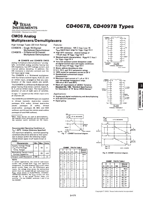
The CD4067B and CD4097B types are suppliedin 24-lead hermetic dual-in-line ceramicpackages (F3A suffix), 24-lead dual-in-lineplastic packages (E suffix), 24-leadsmall-outline packages (M, M96, and NSRsuffixes), and 24-lead thin shrink small-outlinepackages (P and PWR suffixes).Copyright© 2003, Texas Instruments IncorporatedPACKAGING INFORMATIONAddendum-Page 1(1) The marketing status values are defined as follows:ACTIVE: Product device recommended for new designs.LIFEBUY: TI has announced that the device will be discontinued, and a lifetime-buy period is in effect.NRND: Not recommended for new designs. Device is in production to support existing customers, but TI does not recommend using this part in a new design.PREVIEW: Device has been announced but is not in production. Samples may or may not be available.OBSOLETE: TI has discontinued the production of the device.(2) Eco Plan - The planned eco-friendly classification: Pb-Free (RoHS), Pb-Free (RoHS Exempt), or Green (RoHS & no Sb/Br) - please check /productcontent for the latest availability information and additional product content details.TBD: The Pb-Free/Green conversion plan has not been defined.Pb-Free (RoHS): TI's terms "Lead-Free" or "Pb-Free" mean semiconductor products that are compatible with the current RoHS requirements for all 6 substances, including the requirement that lead not exceed 0.1% by weight in homogeneous materials. Where designed to be soldered at high temperatures, TI Pb-Free products are suitable for use in specified lead-free processes.Pb-Free (RoHS Exempt): This component has a RoHS exemption for either 1) lead-based flip-chip solder bumps used between the die and package, or 2) lead-based die adhesive used between the die and leadframe. The component is otherwise considered Pb-Free (RoHS compatible) as defined above.Green (RoHS & no Sb/Br): TI defines "Green" to mean Pb-Free (RoHS compatible), and free of Bromine (Br) and Antimony (Sb) based flame retardants (Br or Sb do not exceed 0.1% by weight in homogeneous material)(3) MSL, Peak Temp. - The Moisture Sensitivity Level rating according to the JEDEC industry standard classifications, and peak solder temperature.(4) There may be additional marking, which relates to the logo, the lot trace code information, or the environmental category on the device.(5) Multiple Device Markings will be inside parentheses. Only one Device Marking contained in parentheses and separated by a "~" will appear on a device. If a line is indented then it is a continuation of the previous line and the two combined represent the entire Device Marking for that device.(6) Lead/Ball Finish - Orderable Devices may have multiple material finish options. Finish options are separated by a vertical ruled line. Lead/Ball Finish values may wrap to two lines if the finish value exceeds the maximum column width.Important Information and Disclaimer:The information provided on this page represents TI's knowledge and belief as of the date that it is provided. TI bases its knowledge and belief on information provided by third parties, and makes no representation or warranty as to the accuracy of such information. Efforts are underway to better integrate information from third parties. TI has taken and continues to take reasonable steps to provide representative and accurate information but may not have conducted destructive testing or chemical analysis on incoming materials and chemicals. TI and TI suppliers consider certain information to be proprietary, and thus CAS numbers and other limited information may not be available for release.Addendum-Page 2In no event shall TI's liability arising out of such information exceed the total purchase price of the TI part(s) at issue in this document sold by TI to Customer on an annual basis.OTHER QUALIFIED VERSIONS OF CD4067B, CD4067B-MIL, CD4097B, CD4097B-MIL :•Catalog: CD4067B, CD4097B•Military: CD4067B-MIL, CD4097B-MILNOTE: Qualified Version Definitions:•Catalog - TI's standard catalog product•Military - QML certified for Military and Defense ApplicationsAddendum-Page 3TAPE AND REELINFORMATION *Alldimensions are nominal Device Package Type Package DrawingPinsSPQ Reel Diameter (mm)Reel Width W1(mm)A0(mm)B0(mm)K0(mm)P1(mm)W (mm)Pin1Quadrant CD4067BM96SOICDW 242000330.024.410.7515.7 2.712.024.0Q1CD4067BM96SOICDW 242000330.024.410.7515.7 2.712.024.0Q1CD4067BM96G4SOICDW 242000330.024.410.7515.7 2.712.024.0Q1CD4067BPWR TSSOPPW 242000330.016.4 6.958.3 1.68.016.0Q1CD4097BPWR TSSOP PW 242000330.016.4 6.958.3 1.68.016.0Q1PACKAGE MATERIALS INFORMATION 24-Oct-2014Pack Materials-Page 1*All dimensionsare nominal DevicePackage Type Package Drawing Pins SPQ Length (mm)Width (mm)Height (mm)CD4067BM96SOIC DW 242000366.0364.050.0CD4067BM96SOIC DW 242000367.0367.045.0CD4067BM96G4SOIC DW 242000367.0367.045.0CD4067BPWRTSSOP PW 242000367.0367.038.0CD4097BPWR TSSOP PW 242000367.0367.038.0PACKAGE MATERIALS INFORMATION 24-Oct-2014Pack Materials-Page 2IMPORTANT NOTICETexas Instruments Incorporated and its subsidiaries(TI)reserve the right to make corrections,enhancements,improvements and other changes to its semiconductor products and services per JESD46,latest issue,and to discontinue any product or service per JESD48,latest issue.Buyers should obtain the latest relevant information before placing orders and should verify that such information is current and complete.All semiconductor products(also referred to herein as“components”)are sold subject to TI’s terms and conditions of sale supplied at the time of order acknowledgment.TI warrants performance of its components to the specifications applicable at the time of sale,in accordance with the warranty in TI’s terms and conditions of sale of semiconductor products.Testing and other quality control techniques are used to the extent TI deems necessary to support this warranty.Except where mandated by applicable law,testing of all parameters of each component is not necessarily performed.TI assumes no liability for applications assistance or the design of Buyers’products.Buyers are responsible for their products and applications using TI components.To minimize the risks associated with Buyers’products and applications,Buyers should provide adequate design and operating safeguards.TI does not warrant or represent that any license,either express or implied,is granted under any patent right,copyright,mask work right,or other intellectual property right relating to any combination,machine,or process in which TI components or services are rmation published by TI regarding third-party products or services does not constitute a license to use such products or services or a warranty or endorsement e of such information may require a license from a third party under the patents or other intellectual property of the third party,or a license from TI under the patents or other intellectual property of TI.Reproduction of significant portions of TI information in TI data books or data sheets is permissible only if reproduction is without alteration and is accompanied by all associated warranties,conditions,limitations,and notices.TI is not responsible or liable for such altered rmation of third parties may be subject to additional restrictions.Resale of TI components or services with statements different from or beyond the parameters stated by TI for that component or service voids all express and any implied warranties for the associated TI component or service and is an unfair and deceptive business practice. TI is not responsible or liable for any such statements.Buyer acknowledges and agrees that it is solely responsible for compliance with all legal,regulatory and safety-related requirements concerning its products,and any use of TI components in its applications,notwithstanding any applications-related information or support that may be provided by TI.Buyer represents and agrees that it has all the necessary expertise to create and implement safeguards which anticipate dangerous consequences of failures,monitor failures and their consequences,lessen the likelihood of failures that might cause harm and take appropriate remedial actions.Buyer will fully indemnify TI and its representatives against any damages arising out of the use of any TI components in safety-critical applications.In some cases,TI components may be promoted specifically to facilitate safety-related applications.With such components,TI’s goal is to help enable customers to design and create their own end-product solutions that meet applicable functional safety standards and requirements.Nonetheless,such components are subject to these terms.No TI components are authorized for use in FDA Class III(or similar life-critical medical equipment)unless authorized officers of the parties have executed a special agreement specifically governing such use.Only those TI components which TI has specifically designated as military grade or“enhanced plastic”are designed and intended for use in military/aerospace applications or environments.Buyer acknowledges and agrees that any military or aerospace use of TI components which have not been so designated is solely at the Buyer's risk,and that Buyer is solely responsible for compliance with all legal and regulatory requirements in connection with such use.TI has specifically designated certain components as meeting ISO/TS16949requirements,mainly for automotive use.In any case of use of non-designated products,TI will not be responsible for any failure to meet ISO/TS16949.Products ApplicationsAudio /audio Automotive and Transportation /automotiveAmplifiers Communications and Telecom /communicationsData Converters Computers and Peripherals /computersDLP®Products Consumer Electronics /consumer-appsDSP Energy and Lighting /energyClocks and Timers /clocks Industrial /industrialInterface Medical /medicalLogic Security /securityPower Mgmt Space,Avionics and Defense /space-avionics-defense Microcontrollers Video and Imaging /videoRFID OMAP Applications Processors /omap TI E2E Community Wireless Connectivity /wirelessconnectivityMailing Address:Texas Instruments,Post Office Box655303,Dallas,Texas75265Copyright©2014,Texas Instruments Incorporated。