4395A 阻抗分析仪使用方法
电阻测试仪使用方法说明书

电阻测试仪使用方法说明书一、概述电阻测试仪是一种用于测量电路中电阻值的设备,广泛应用于电子工程、电力系统、通信设备等领域。
本说明书旨在详细介绍电阻测试仪的使用方法,帮助用户正确、高效地操作设备。
二、设备介绍1. 外观描述电阻测试仪外观精致紧凑,有LCD显示屏、操作按键和测试接口。
设备采用优质材料制造,具有防震、防尘、防滑等特性,便于携带和使用。
2. 技术指标- 测量范围:0.01Ω - 10MΩ- 准确度:±1%- 工作电压:220V AC- 重复性:0.5%- 工作温度:0°C - 40°C三、操作步骤1. 准备工作确保电阻测试仪电源正常连接,并插入合适的电源插座。
待设备开机启动完成后,显示屏将会显示主界面。
2. 测试接线将待测试的电路中的电阻器按电阻值大小依次连接到电阻测试仪的测试接口上。
确保电路连接牢固、接触良好,避免松动或接触不良导致测试结果不准确。
3. 设置测试参数根据待测电路的特性,合理设置测试仪的参数。
通过操作按键,进入设置界面,选择合适的测量范围和精度,并根据需要设置温度补偿等功能。
确认设置后,返回主界面。
4. 进行测试按下“开始”按钮,电阻测试仪将开始自动进行测试。
待测试完成后,显示屏将显示测得的电阻值,并给出相应的测试结果。
用户可根据需要将结果记录下来或进行其他操作。
5. 关机测试完成后,根据需要选择合适的关机方式。
长按电源按钮进行强制关机,或通过菜单中的关机选项进行正常关机。
四、注意事项1. 在使用电阻测试仪前,确保自身安全,例如需要戴好绝缘手套,避免触电危险。
2. 在测试过程中,尽量避免与测试接线触碰,以免干扰测试结果。
3. 预热时间可能会影响测试结果。
在首次开机或长时间未使用后,建议进行一段时间的预热操作。
4. 若测试结果与预期不符,建议检查测试接线是否正确连接或考虑是否需要更换电阻器。
五、维护与保养1. 定期清洁电阻测试仪外壳,使用干净的柔软布进行擦拭,避免使用化学溶剂。
4395A网络分析仪设备操作规范

核准
仪器名称 仪器型号
审核
制作
仪器设备操作规范
网络分析仪
HP4395A
测试项目 厂商
特性 安捷伦
日期
第4页 共4页
文件编号
版本/次
B0
2.2 如某产品归零方法有异﹐工程部另行通知﹔ 2.3 如操作失败请重新按步骤操作﹔ 2.4 如有异常现象及时通知相关人员﹐严禁私自乱调﹑乱修。 3. 维护保养﹕ 3.1 保持机身清洁﹔ 3.2 搬动仪器时轻拿轻放﹔ 3.3 禁用带腐浊性溶剂擦仪器﹔ 3.4 不用时要及时关机。
Cal
校正归零
Recall
读取数据
Sweep
扫描设定
Utility
显示模式
Line
电源开关
Local
外加电压
1.3 测试模式设定﹕ 1.3.1 打开电源开关 LINE 仪器自检﹔ 1.3.2 按面板 Meas 按软功能键 Analyzer Type
选择 NETWORK ANALYZER﹔
1.3.3 Insertion Loss 设定模式﹕Chan1 按 Meas 选择 B/R﹔ 1.3.4 Return Loss 设定模式﹕按面板 Chan2 按 Meas 选择 A/R﹔ 1.4 起始及结束频率设定﹕ 1.4.1 输入起始频率(如 10K/M)﹕按面板 Start 按数字键 10 按单位键 K/M﹔ 1.4.2 输入结束频率(如 9M/u)﹕按面板 Stop 按数字键 9 按单位键 M/u﹔ 1.5 扫描频率设定(如 300X1)﹕按面板 BW/AVG 按数字键 300 按单位键 X1 1.6 画面显示设定﹕按面板 Utility MAK LIST 选择 ON off﹔ 1.7 系统数据设定﹕ 1.7.1 输入限制线频率点(如 900KHz): System LIMIT Menu EDIT LIMIT LINE
阻抗测试仪测试方法

阻抗测试仪测试方法
宝子们,今天咱们来唠唠阻抗测试仪的测试方法哈。
然后呢,找到咱要测试的东西。
比如说要测个小零件啥的,得把这个零件稳稳当当放在合适的地方。
如果是那种电路板上的小元件,可得小心着点,别把周围其他东西给弄坏了。
接着就开始连接啦。
把测试仪的测试线接到要测试的物件上,这就像给它们牵上了小绳子一样。
要确保连接得紧紧的,松松垮垮的话,那测出来的数据可就不准喽,就像你走路不稳当老是摔跤一样,数据也会“摔跤”变得不靠谱。
再之后呢,打开阻抗测试仪的电源。
这时候测试仪就像被唤醒的小机器人一样开始工作啦。
有些测试仪可能还有一些初始的设置要调整,比如说测量的范围之类的。
咱就按照实际的需求来调整,就像给小机器人下指令一样,告诉它我们要怎么测。
等这些都弄好,就可以开始正式测试啦。
看着测试仪上的数值一点点显示出来,是不是还有点小激动呢。
如果数值稳定下来了,那这个数值就是咱要的阻抗值啦。
要是测试完了,可别着急走哦。
把测试线从测试物件上小心翼翼地取下来,就像解开小绳子一样。
然后把测试仪也好好收拾一下,关闭电源,把线都整理好。
这样下次要用的时候,它还是整整齐齐的,随时可以再“战斗”呢。
宝子们,阻抗测试仪的测试方法其实也不难啦,只要细心一点,按照这个步骤来,肯定能测好的。
Agilent 4395A 网络 频谱 阻抗分析仪数据手册说明书
Network Measurement1.At relative to 0 dBm output, 50 MHz,23 °C ±5 °C /HP-Agilent-4395A-Spectrum-Network-Analyzer.aspx To buy, sell, rent or trade-in this product please click on the link below:2Network MeasurementcontinuedReceiver CharacteristicsInput characteristicsFrequency range . . . . . . . . . . . . . . . . . . . . . . . . . . . . . . . . . . . . . . . . . . .10 Hz to 500 MHzInput attenuator . . . . . . . . . . . . . . . . . . . . . . . . . . . . . . . . . . . . . . . . .0 to 50 dB, 10 dB stepFull scale input level (R, A, B)Attenuator setting (dB) Full scale input level0–10 dBm100 dBm20+10 dBm30+20 dBm40+30 dBm50+30 dBmIF bandwidth (IFBW)2, 10, 30, 100, 300, 1 k, 3 k, 10 k, 30 kHzNote: The IFBW should be set to less than 1/5 of the lowest frequency inthe sweep range.Noise level (referenced to full scale input level, 23 °C ±5 °C)at 10 Hz ≤frequency < 100 Hz, IFBW = 2 Hz . . . . . . . . . . . . . . . . . . . . . .–85 dB (SPC)at 100 Hz ≤frequency < 100 kHz, IFBW = 10 Hz . . . . . . . . . . . . . . . . . . . . . . . . .–85 dBat 100 kHz ≤frequency, IFBW = 10 Hz . . . . . . . . . . . . . . . . . . . . . . . . . . . . . .-–115 dBInput crosstalkfor input R + 10 dBm input, input attenuator: . . . . . . . . . . . . . . . . . . . . . . . . . . . . .20 dBfor input A, B input attenuator: . . . . . . . . . . . . . . . . . . . . . . . . . . . . . . . . . . . . . . . . .0 dBat < 100 kHzR through A, B . . . . . . . . . . . . . . . . . . . . . . . . . . . . . . . . . . . . . . . . . . . . . .< –100 dBothers . . . . . . . . . . . . . . . . . . . . . . . . . . . . . . . . . . . . . . . . . . . . . . .< –100 dB (SPC)at ≥100 kHzR through A, B . . . . . . . . . . . . . . . . . . . . . . . . . . . . . . . . . . . . . . . . . . . . .< –120 dBothers . . . . . . . . . . . . . . . . . . . . . . . . . . . . . . . . . . . . . . . . . . . . . . .< –120 dB (SPC)Source crosstalk (for input A, B)(typical for input R)at + 10 dBm output, < 100 kHz, input attenuator: 0 dB . . . . . . . . . . . . . . . . .< –100 dBat + 10 dBm output, ≥100 kHz, input attenuator: 0 dB . . . . . . . . . . . . . . . . .< –120 dBMultiplexer switching impedance changeat input attenuator 0 dB . . . . . . . . . . . . . . . . . . . . . . . . . . . . . . . . . . . . . . . .< 0.5% (SPC)at input attenuator 10 dB and above . . . . . . . . . . . . . . . . . . . . . . . . . . . . . .< 0.1% (SPC)Connector . . . . . . . . . . . . . . . . . . . . . . . . . . . . . . . . . . . . . . . . . . . . . . . . . . . .Type-N femaleImpedance . . . . . . . . . . . . . . . . . . . . . . . . . . . . . . . . . . . . . . . . . . . . . . . . . . . .50 ΩnominalReturn lossInput attenuator0 dB10 dB20 dB to 50 dB10 Hz ≤frequency < 100 kHz25 dB125 dB125 dB1100 kHz ≤frequency ≤100 MHz25 dB125 dB25 dB1100 MHz < frequency15 dB115 dB15 dB1Maximum input level+30 dBm (at input attenuator: 40 dB or 50 dB)Maximum safe input level+30 dBm or ±7 Vdc (SPC)1.SPC34Absolute amplitude accuracy (R, A, B)at –10 dBm input, input attenuator:10 dB, frequency ≥100 Hz, IFBW ≤3 kHz, 23 °C ±5 °C, . . . . . . . . . . . .< ±1.5 dB Ratio accuracy (A/R, B/R) (typical for A/B)at –10 dBm input, input attenuator:10 dB, IFBW ≤3 kHz, 23 °C ±5 °C, . . . . . . . . . . . . . . . . . . . . . . . . . . . . . . .< ±2 dB Dynamic accuracy (A/R, B/R) (typical for A/B)Input level Dynamic accuracy 1(relative to full scale input level)frequency ≥100 Hz 0 dB ≥input level > –10 dB ±0.4 dB –10 dB ≥input Level ≥–60 dB ±0.05 dB –60 dB > input level ≥–80 dB ±0.3 dB –80 dB > input level ≥–100 dB ±3 dB Figure 1-1. Magnitude dynamic accuracy Residual responses . . . . . . . . . . . . . . . . . . . . . . . . . . . . . . . . . . .< –80 dB full scale (SPC)Trace noise (A/R, B/R, A/B)at 50 MHz, both inputs: full scale input level –10 dB, IFBW = 300 Hz . . . . . . . . . . . . . .< 0.005 dB rms (SPC)Stability (A/R, B/R, A/B) . . . . . . . . . . . . . . . . . . . . . . . . . . . . . . . .< ±0.01 dB/°C (SPC)Phase characteristics Measurements format . . . . . . . . . . . . . . . . . . .Standard format, expanded phase format Frequency response (deviation from linear phase) (A/R, B/R) (SPC for A/B) at –10 dBm input, input attenuator: 10 dB, IFBW ≤3 kHz, 23 °C ±5 °C . . . . . .< ±12°Dynamic accuracy (A/R, B/R) (SPC for A/B)Input level Dynamic accuracy 1(relative to full scale input level)frequency ≥100 Hz 0 dB ≥input level > –10 dB ±3°–10 dB ≥input Level ≥–60 dB ±0.3°–60 dB > input level ≥–80 dB ±1.8°–80 dB > input level ≥–100 dB ±18°Magnitude Characteristics1.R input level (B input level for A/B) = fullscale input level –10 dB, IFBW = 10 Hz,23 °C ± 5 °CInput level (dB)Magnitude dynamic accuracy D y n a m i c a c c u r a c y (d B )Spec Typical5Figure 1-2. Phase dynamic accuracyTrace noise (A/R, B/R, A/B)at 50 MHz, both inputs:full scale input level –10 dB, IFBW = 300 Hz . . . . . . . . . . . . . . . . .< 0.04°rms (SPC)Stability (A/R, B/R, A/B) . . . . . . . . . . . . . . . . . . . . . . . . . . . . . . . . . . .< ±0.1 °/°C (SPC)Group delay characteristicsAperture [Hz] . . . . . . . . . . . . . . . . . . . . . . . . . . . . . . . . . . . . . . . . . . .0.25% to 20% of span AccuracyIn general, the following formula can be used to determine the accuracy, in seconds,of a specific group delay measurement: . . . . . . . . . . . .Phase accuracy (degree)Aperture(Hz) x 360 (degree)Sweep characteristicsSweep type . . . . . . . . . . . . . . . . .Linear frequency, log frequency, power, list frequency Sweep direction . . . . . . . . . . . . . . . . . . . . . . . . . . . . . . . . . . . . . . . . . .Upper direction only Trigger type . . . . . . . . . . . . . . . . . . . . . . . . . .Hold, single, number of groups, continuous Trigger source . . . . . . . . . . . . . . . . . . . .Internal (free run), external, manual, GPIB (bus)Event trigger . . . . . . . . . . . . . . . . . . . . . . . . . . . . . . . . . . . . . . . . . . . . . .On point, on sweepInput level (dB)Phase dynamic accuracyD y n a m i c a c c u r a c y (d e g r e e )Spec Typical6Frequency characteristics Frequency range . . . . . . . . . . . . . . . . . . . . . . . . . . . . . . . . . . . . . . . . . . .10 Hz to 500 MHz Frequency readout accuracy . . . . . . . .±((freq readout [Hz ]) x (freq ref accuracy [1]) + RBW [Hz ] + SPAN [Hz ])) [Hz ]where NOP means number of display points NOP -1Frequency reference (Option 4395A-800)Accuracy at 23 °C ±5 °C, referenced to 23 °C . . . . . . . . . . . . . . . . . . . . . . . . . . . . .< ±5.5 ppm Aging . . . . . . . . . . . . . . . . . . . . . . . . . . . . . . . . . . . . . . . . . . . . .< ±2.5 ppm/year (SPC) Initial achievable accuracy . . . . . . . . . . . . . . . . . . . . . . . . . . . . . . . .< ±1.0 ppm (SPC) Temperature stability at 23 °C ±5 °C, referenced to 23 °C . . . . . . . . . . . . . . . . . . . . . . . . .< ±2 ppm (SPC) Precision frequency reference (Option 4395A-1D5) Accuracy at 0 °C to 40 °C, referenced to 23 °C . . . . . . . . . . . . . . . . . . . . . . . . . . .< ±0.13 ppm Aging . . . . . . . . . . . . . . . . . . . . . . . . . . . . . . . . . . . . . . . . . . . . . . . . .< ±0.l ppm/year (SPC)Initial achievable accuracy . . . . . . . . . . . . . . . . . . . . . . . . . . . . . . . . .< ±0.02 ppm (SPC)Temperature stability at 0 °C to 40 °C, referenced to 23 °C . . . . . . . . . . . . . . . . . . . . . . . .< ±0.01 ppm (SPC)Resolution bandwidth (RBW)Range 3 dB RBW at span > 0 . . . . . . . . . . . . . . . . . . . . . . . . . . . . . .1 Hz to 1 MHz, 1-3 step 3 dB RBW at span = 0 . . . . . . . . . . . .3 k, 5 k, 10 k, 20 k, 40 k, 100 k, 200 k, 400 k, 800 k, 1.5 M, 3 M, 5 MHz Selectivity (60 dB BW/3 dB BW)at span > 0 . . . . . . . . . . . . . . . . . . . . . . . . . . . . . . . . . . . . . . . . . . . . . . . . . . . . . . . .< 3Mode . . . . . . . . . . . . . . . . . . . . . . . . . . . . . . . . . . . . . . . . . . . . . . . . . . . . .Auto or manual Accuracy at span > 0 . . . . . . . . . . . . . . . . . . . . . . . . . . . . . . . . . . . . . . . . . . . . . . . . . . . .< ±10%at span = 0 . . . . . . . . . . . . . . . . . . . . . . . . . . . . . . . . . . . . . . . . . . . . . . . . . . . .< ±30%Video bandwidth (VBW)Range at span > 0 . . . . . . . . . . . . . . . .3 MHz to 3 MHz, 1-3 step, 0.003 ≤VBW/RBW ≤1Noise sidebands Offset from carrier Noise sidebands ≥1 kHz < –95 dBc/Hz ≥100 kHz < –108 dBc/Hz Figure 1-3. Noise sidebandsSpectrum Measurement Frequency offset [Hz]N o i s e s i d e b a n d [d B c /H z ]Spec Typical7Amplitude range . . . . . . . . . . . . . . . . . . . . . . . . . .displayed average noise level to +30 dBm Reference value setting range . . . . . . . . . . . . . . . . . . . . . . . . . . . . . .–100 dBm to +30 dBm Level accuracy at –20 dBm input, 50 MHz, input attenuator: 10 dB, 23 °C ±5 °C . . . . . . . . . . .< ±0.8 dB Frequency response at -20 dBm input, input attenuator: 10 dB, referenced to level at 50 MHz, 23 °C ±5 °C frequency ≥100 Hz . . . . . . . . . . . . . . . . . . . . . . . . . . . . . . . . . . . . . . . . . . . . . .< ±1.5 dB frequency < 100 Hz . . . . . . . . . . . . . . . . . . . . . . . . . . . . . . . . . . . . . . . . . . . . . .< ±1.3 dB Amplitude fidelity 1Log scale 2Range Amplitude fidelity (dB to reference input lever [dB][dB]0 to –30±0.05–30 to –40±0.07–40 to –50±0.15–50 to –60±0.35–60 to –70±0.8–70 to –80±1.8Linear scale 2 . . . . . . . . . . . . . . . . . . . . . . . . . . . . . . . . . . . . . . . . . . . . . . . . . . . . . . . . . . .< ±3%Displayed average noise level at reference value ≤–40 dBm, input attenuator: auto or 0 dB at frequency ≥1 kHz . . . . . . . . . . . . . . . . . . . . . . . . . . . . . . . . . . . . . . . . . . . .–120 dBm/Hz at ≥100 kHz . . . . . . . . . . . . . . . . . . . . . . . . . . . . . . . . . . . . . . . . . . . . . . . . . . .–133 dBm/Hz at ≥10 MHz . . . . . . . . . . . . . . . . . . . . . . . . . . . . .(–145 + frequency/100 MHz) dBm/Hz 3Figure 1-4. Typical displayed average noise level Amplitude Characteristics1.Fidelity shows an extent of nonlinearity referenced to the reference input level.2.RBW = 10 Hz, –20 dBm ≤reference value ≤+30 dBm, reference input level = full scale input level –10 dB, 23 ±5 °C3. At start frequency ≥10 MHzNote: Refer to Input attenuator part for the definition of full scale input level.Frequency offset [Hz]A v e r a g e n o i s e l e v e l [d B m /H z ]SpecTypical8Figure 1-5. Typical on-screen dynamic range (center: 100 MHz)Spurious responses Second harmonic distortion at single tone input with full scale input level –10 dB, input signal frequency ≥100 kHz . . . . . . . . . . . . . . . . . . . . . . . . . . . . . . . . . . . . . . . . . . .< –70 dBc, < –75 dBc (SPC)Third order inter-modulation distortion at two tones input with full scale input level –16 dB, separation ≥100 kHz . . . . . . . . . . . . . . . . . . . . . . . . . . . . . . . . . . . . . . . . . . . .< –75 dBc, < 80 dBc (SPC)Spurious at single tone input with full scale input level –10 dB, input signal frequency ≤500 MHz . . . . . . . . . . . . . . . . . . . . . . . . . . . . . . . . . . . . . . . . . . . . . . . . . . . . . . . . . .< –75 dBc except for the following frequency ranges:5.6 MHz ±1 MHz, 30.6 MHz ±1 MHz, 415.3 MHz ±1 MHz Residual response at reference value setting ≤–40 dBm, input attenuator: auto or 0 dB . . . . .< –110 dBmOn-screen Dynamic Range Offset frequency [Hz]O n -s c r e e n d y n a m i c r a n g e [d B c ]9Figure 1-6. Typical dynamic range at inputs R, A, and B Input attenuator Setting range . . . . . . . . . . . . . . . . . . . . . . . . . . . . . . . . . . . . . . . .0 dB to 50 dB, 10 dB step Attenuator setting (dB) Full scale input level 0–20 dBm 10–10 dBm 200 dBm 30+10 dBm 40+20 dBm 50+30 dBm Mode . . . . . . . . . . . . . . . . . . . . . . . . . . . . . . . . . . . . . . . . . . . . . . . . . . . . . . . . .Auto or manual (In auto mode, the attenuator is set to 20 dB above the reference value; this ensures that the maximum signal level after the attenuator will not be greater than –20 dBm.)Input attenuator switching uncertainty at attenuator: ≤30 dB, referenced to 10 dB . . . . . . . . . . . . . . . . . . . . . . . . . . . . .< ±1.0 dB at attenuator: ≥40 dB, referenced to 10 dB . . . . . . . . . . . . . . . . . . . . . . . . . . . .< ±1.5 dB Temperature drift . . . . . . . . . . . . . . . . . . . . . . . . . . . . . . . . . . . . . . . . . .< ±0.05 dB/°C (SPC)Scale Log 0.1 dB/div to 20 dB/div Linear at watt . . . . . . . . . . . . . . . . . . . . . . . . . . . . . . . . . . . . . . . . . . . . . . . . . . .1.0 x 10-12W/div at volt . . . . . . . . . . . . . . . . . . . . . . . . . . . . . . . . . . . . . . . . . . . . . . . . . . . . .1.0 x 10-9V/div Measurement format . . . . . . . . . . . . . . . . . . . . . . . . . . . . . . . . . . . . .Spectrum or noise (/Hz) Display unit . . . . . . . . . . . . . . . . . . . . . . . . . . . .dBm (unit of marker: dBm, dBV, dBµV, V, W)Sweep characteristics Sweep type . . . . . . . . . . . . . . . . . . . . . . . . . . . . . . . . . . . . . . . . . . . . . . . . . . . . . .Linear, list Trigger type . . . . . . . . . . . . . . . . . . . . . . . . . . .Hold, single, number of groups, continuous Trigger source . .Internal (free run), external, manual, level gate, edge gate, GPIB (bus)Sweep time (excluding each sweep setup time)RBW SPAN Typical sweep time 1 MHz 500 MHz 190 ms 100 kHz 100 MHz 300 ms 10 kHz 10 MHz 240 ms 1 kHz 1 MHz 190 ms 100 Hz 100 kHz 270 ms 10 Hz 10 kHz 2.0 s 1 Hz 1 kHz 11 s—Zero Span —1Typical Dynamic Range1.See the next item for sweep time at zero span Input level (dB)(Relative to full scale input level)D y n a m i c r a n g e (d B )Sensitivity (1 Hz RBW)Sensitivity ( 100 Hz RBW)2nd harmonic distortion 3rd order inter-modulation distortion Second Third1011Gate lengthRange . . . . . . . . . . . . . . . . . . . . . . . . . . . . . . . . . . . . . . . . . . . . . . . . . . . . . . .6 µs to 3.2 s ResolutionRange of gate length (T I )Resolution 6 µs ≤T I ≤25 ms 0.4 µs 25 ms < T I ≤64 ms 1 µs 64 ms < T I ≤130 ms 2 µs 130 ms < T I ≤320 ms 5 µs 320 ms < T I ≤1.28 s 20 µs 1.28s < T I ≤3.2 s100 µsGate lengthRange . . . . . . . . . . . . . . . . . . . . . . . . . . . . . . . . . . . . . . . . . . . . . . . . . . . . . . .2 µs to 3.2 sResolutionRange of gate delay (T d )Resolution 2 µs ≤T d ≤25 ms 0.4 µs 25 ms < T d ≤64 ms 1 µs 64 ms <T d ≤130 ms 2 µs 130 ms < T d ≤320 ms 5 µs 320 ms < T d ≤1.28 s 20 µs 1.28 s < T d ≤3.2 s100 µsAdditional amplitude errorLog scale . . . . . . . . . . . . . . . . . . . . . . . . . . . . . . . . . . . . . . . . . . . . . . . . . .< 0.3 dB (SPC)Linear scale . . . . . . . . . . . . . . . . . . . . . . . . . . . . . . . . . . . . . . . . . . . . . . . . . .< 3% (SPC)Gate control modes . . . . . . . . . . . . . . . . . . . . . . . . . . . . .Edge (positive/negative) or level Gate trigger input (external trigger input is used)Connector . . . . . . . . . . . . . . . . . . . . . . . . . . . . . . . . . . . . . . . . . . . . . . . . . . . .BNC female Level . . . . . . . . . . . . . . . . . . . . . . . . . . . . . . . . . . . . . . . . . . . . . . . . . . . . . . . . . . . . . . .TTL Gate outputConnector . . . . . . . . . . . . . . . . . . . . . . . . . . . . . . . . . . . . . . . . . . . . . . . . . . . .BNC female Level . . . . . . . . . . . . . . . . . . . . . . . . . . . . . . . . . . . . . . . . . . . . . . . . . . . . . . . . . . . . . . . .TTLSpecifications when Option 4395A-1D6 Time-Gated Spectrum Analysis is InstalledAll specifications are identical to the standard Agilent 4395A except the following items.12Measurement functions Measurement parameters Z, Y, L, C, Q, R, X, G, B, θDisplay parameters IZI, 0z , R, X, IYI, θy , G, B, I ΓI, θγ, Γx , Γy , Cp, Cs,Lp, Ls, Rp, Rs, D, QDisplay formats•Vertical lin/log scale •Complex plane•Polar/Smith/admittance chart Sweep parameters•Linear frequency sweep•Logarithmic frequency sweep •List frequency sweep•Power sweep (in dBm unit)IF bandwidth•2,10, 30, 100, 300, 1k, 3k, 10k, 30k [Hz]Calibration•OPEN/SHORT/LOAD 3 term calibration •Fixture compensation •Port extension correction Measurement port type •7-mm Output characteristicsFrequency range . . . . . . . . . . . . . . . . . . . . . . . . . . . . . . . . . . . . . . . . . .100 kHz to 500 MHz Frequency resolution . . . . . . . . . . . . . . . . . . . . . . . . . . . . . . . . . . . . . . . . . . . . . . . . .1 MHz Output impedance . . . . . . . . . . . . . . . . . . . . . . . . . . . . . . . . . . . . . . . . . . . . .50 Ωnominal Output levelwhen the measurement port is terminated by 50 Ω1 . . . . . . . . . . . . . .–56 to +9 dBm when the measurement port is open . . . . . . . . . . . . . . . . . . .0.71 mVrms to 1.26 Vrms Resolution . . . . . . . . . . . . . . . . . . . . . . . . . . . . . . . . . . . . . . . . . . . . . . . . . . . . . . . . . . .0.1 dBm Level accuracy . . . . . . . . . . . . . . . . . . . . . . . . . . . . . . . . . . . .±(A + B + 6 x F/(1.8 x 109))dB WhereA = 2 dBB = 0 dB (at 0 dBm ≤P ≤+ 15 dBm) or B = 1 dB (at –40 dBm ≤P < 0 dBm) or B = 2 dB (at –50 dBm ≤P < –40 dBm)F is setting frequency [Hz], P is output power settingOption 4395A-010Impedance measurementThe following specifications are applied when the 43961A impedance test kit is connected to the 4395A.1.When the measurement port is terminated with 50 Ω, the signal level at the measure-ment port is 6 dB lower than the signal level at the RF OUT port.13Measurement accuracy is specified at the connecting surface of the 7-mm connector of the Agilent 43961A under the following conditions:Warm up time . . . . . . . . . . . . . . . . . . . . . . . . . . . . . . . . . . . . . . . . . . . . . . . . .> 30 minutes Ambient temperature . . . . . . . . . . . . . . . . . . . . . . . . . . . . . . . . . . . . . . . . . . . .23 °C ±5 °C,within ±1 °C from the temperature at which calibration is performedSignal level (setting) . . . . . . . . . . . . . . . . . . . . . . . . . . . . . . . . . . . . . . . . . . .0 to +15 dBm Correction . . . . . . . . . . . . . . . . . . . . . . . . . . . . . . . . . . . . . . . . . . . . . . . . . . . . . . . . . . . . .ON IFBW (for calibration and measurement) . . . . . . . . . . . . . . . . . . . . . . . . . . . . . .≤300 Hz Averaging factor (for calibration and measurement) . . . . . . . . . . . . . . . . . . . . . . . . .≥8Figure 1-7. Impedance measurement accuracyIZI - θaccuracy IZI accuracy Z a = A + (B /I Z m I + C x I Z m I) x 100 [%]θaccuracy θa = sin -1(Z a /100)Where, I Z m I is I Z I measured. A, B, and C are obtained from Figure 1-7.IYI - θaccuracy IYI accuracy Y a = A + (B x I Y m I + C /I Z m I) x 100 [%]θaccuracy θa = sin -1(Y a /100)Where, I Y m I is I Y I measured. A, B, and C are obtained from Figure 1-7.Measurement Basic Accuracy(Supplemental performancecharacteristics)Test frequency [Hz]14Display LCDSize/type . . . . . . . . . . . . . . . . . . . . . . . . . . . . . . . . . . . . . . . . . . . . . . .8.4 inch color LCD Number of pixels . . . . . . . . . . . . . . . . . . . . . . . . . . . . . . . . . . . . . . . . . . . . . . . .640 x 480Effective display area . . . . . . . . . . . . . . . . . . . . . . .160 mm x 115 mm(600 x 430 dots)Number of display channels . . . . . . . . . . . . . . . . . . . . . . . . . . . . . . . . . . . . . . . . . . . . .2Format single, dual (split or overwrite)Number of traces . . . . . . . . . . . . . . . . . . . . . . . . . . . . . . . . . . . . . . . . . . . . . . . . . . . . . . . . . .For measurement . . . . . . . . . . . . . . . . . . . . . . . . . . . . . . . . . . . . . . . . . . . . . . . . .2 traces For memory . . . . . . . . . . . . . . . . . . . . . . . . . . . . . . . . . . . . . . . . . . . . . . . . . . . . . .2 traces Data math . . . . . . . . . . . . . . . . . . . . . . . . . . . . . . . . . . . . . . . . . . . . . . .gain x data – offset,gain x (data - memory) – offset,gain x (data + memory) – offset,gain x (data/memory ) – offsetData hold . . . . . . . . . . . . . . . . . . . . . . . . . . . . . . . . . . . . . . .Maximum hold, minimum hold MarkerNumber of markersMain marker . . . . . . . . . . . . . . . . . . . . . . . . . . . . . . . . . . . . . . . . . . . .l for each channel Sub-marker . . . . . . . . . . . . . . . . . . . . . . . . . . . . . . . . . . . . . . . . . . . . .7 for each channel ∆marker . . . . . . . . . . . . . . . . . . . . . . . . . . . . . . . . . . . . . . . . . . . . . . .1 for each channel Hard copyMode . . . . . . . . . . . . . . . . . . . . . . . . . . . .Dump mode only (including color dump mode)StorageBuilt-in flexible disk driveType . . . . . . . . . . . . . . . . . . . . . . . . . . . . . . . . . . . . . .3.5 inch, 1.44 MByte, or 720 KByte,1.44 MByte format is used for disk initializationMemory . . . . . . . . . . . . . . . . . . . . . . . . . . .512 KByte, can be backed up by flash memory GPIBInterface . . . . . . . . . . . . . . . . . . . . . . . . . . . . . . . . . . . . .IEEE 488.1-1987, IEEE 488.2-1987,IEC 625, and JIS C 1901-1987 standards compatible.Interface function . . . . . . . . . . . . . . . . . . . . . . . . .SH1, AH1, T6, TEO, L4, LEO, SR1, RL1,PP0, DC1, DT1, C1, C2, C3, C4, C11, E2Data transfer formats . . . . . . . . . . . . . . . . . . . . . . . . . . . . . . . . . . . . . . . . . . . . . . . . .ASCII,32 and 64 bit IEEE 754 floating point format,DOS PC format (32 bit IEEE with byte order reversed)Printer parallel portInterface . . . . . . . . . . . . . . . . . . . . . . . . . . . . . . .IEEE 1284 Centronics standard compliant Printer control language . . . . . . . . . . . . . . . . . . . . . . . . . . .PCL3 printer control language Connector . . . . . . . . . . . . . . . . . . . . . . . . . . . . . . . . . . . . . . . . . . . . . . . . . . .D-SUB (25-pin)15Common toNetwork/Spectrum/Impedance Measurement16Option 4395A-001 DC voltage/current sourceThe setting of Option 4395A-001 DC voltage/current source is independent of channel 1 and channel 2 settings.VoltageRange . . . . . . . . . . . . . . . . . . . . . . . . . . . . . . . . . . . . . . . . . . . . . . . . . . . . .–40 V to +40 V Resolution . . . . . . . . . . . . . . . . . . . . . . . . . . . . . . . . . . . . . . . . . . . . . . . . . . . . . . . . .1 mV Current limitationat voltage setting = –25 V to +25 V . . . . . . . . . . . . . . . . . . . . . . . . . . . . . .±100 mAat voltage setting = –40 V to –25 V, 25 V to 40 V . . . . . . . . . . . . . . . . . . .±20 mA CurrentRange–20 µA to -100 mA, 20 µA to 100 mAResolution . . . . . . . . . . . . . . . . . . . . . . . . . . . . . . . . . . . . . . . . . . . . . . . . . . . . . . . . . . .20 µA Voltage limitationat current setting = –20 mA to +20 mA . . . . . . . . . . . . . . . . . . . . . . . . . . . . . . .±40 V at current setting = –100 mA to –20 mA, 20 mA to 100 mA . . . . . . . . . . . . . .±25 V AccuracyVoltageat 23 °C ±5 °C . . . . . . . . . . . . . . . . . . . . . . .±(0.1% + 4 mV + I dc1[mA] x 5 [Ω] mV) Currentat 23 °C ±5 °C . . . . . . . . . . . . . . . . . . . . . . .±(0.5% + 30 µA + V dc2[V]/10 [kΩ] mA) Probe powerOutput voltage . . . . . . . . . . . . . . . . .+15 V (300 mA), –12.6 V (160 mA), GND nominal Specifications when instrument BASIC is operatedKeyboard . . . . . . . . . . . . . . . . . . . . . . . . . . . . . . . . . . . . .PS/2 style 101 English keyboard Connector . . . . . . . . . . . . . . . . . . . . . . . . . . . . . . . . . . . . . . . . . . . . . . . . . . . . . .mini-DIN 8 bit I/0 portConnector . . . . . . . . . . . . . . . . . . . . . . . . . . . . . . . . . . . . . . . . . . . . . . . . .D-SUB (15-pin) Level . . . . . . . . . . . . . . . . . . . . . . . . . . . . . . . . . . . . . . . . . . . . . . . . . . . . . . . . . . . . . . .TTL Number of input/output bit . . . . . . . . . . . . . . . . . . . . . .4 bit for input, 8 bit for outputFigure 1-8. 8 bit I/O port pin assignments24-bit I/O interfaceConnector . . . . . . . . . . . . . . . . . . . . . . . . . . . . . . . . . . . . . . . . . . . . . . . . . . .D-SUB (36-pin) Level . . . . . . . . . . . . . . . . . . . . . . . . . . . . . . . . . . . . . . . . . . . . . . . . . . . . . . . . . . . . . . . . .TTL I/O . . . . . . . . . . . . . . . . . . . . . . . . . . . . . . . . . . .8-bit for input or output, 16-bit for output Figure 1-9. 24-bit I/O interface pin assignment1.Current at DC source connector.2.Voltage at DC source connector.Table 1-1. Signal source assignmentPin No. Signal name Signal standard1GND0 V2INPUT1TTL level, pulse input (pulse width: 1 µs or above) 3OUTPUT1TTL level, latch output4OUTPUT2TTL level, latch output5OUTPUT PORT A0TTL level, latch output6OUTPUT PORT A1TTL level, latch output7OUTPUT PORT A2TTL level, latch output8OUTPUT PORT A3TTL level, latch output9OUTPUT PORT A4TTL level, latch output10OUTPUT PORT A5TTL level, latch output11OUTPUT PORT A6TTL level, latch output12OUTPUT PORT A7TTL level, latch output13OUTPUT PORT B0TTL level, latch output14OUTPUT PORT B1TTL level, latch output15OUTPUT PORT B2TTL level, latch output16OUTPUT PORT B3TTL level, latch output17OUTPUT PORT B4TTL level, latch output18OUTPUT PORT B5TTL level, latch output19OUTPUT PORT B6TTL level, latch output20OUTPUT PORT B7TTL level, latch output21I/O PORT C0TTL level, latch output22I/O PORT C1TTL level, latch output23I/O PORT C2TTL level, latch output24I/O PORT C3TTL level, latch output25I/O PORT D0TTL level, latch output26I/O PORT D1TTL level, latch output27I/O PORT D2TTL level, latch output28I/O PORT D3TTL level, latch output29PORT C STATUS TTL level, input mode: LOW, output mode: HIGH 30PORT D STATUS TTL level, input mode: LOW, output mode: HIGH 31WRITE STROBE SIGNAL TTL level, active low, pulse output(width: 10 µs; typical)32+5 V PULLUP33SWEEP END SIGNAL TTL level, active low, pulse output(width: 20 µs; typical)34+5 V+5 V, 100 mA MAX35PASS/FAIL SIGNAL TTL level, PASS: HIGH, FAIL: LOW, latch output36PASS/FAIL WRITE STROBE SIGNALTTL level, active low, pulse output(width: 10 µs; typical)1718Input and output characteristicsExternal reference inputFrequency . . . . . . . . . . . . . . . . . . . . . . . . . . . . . . . . . . . . . . . . . .10 MHz ±100 Hz (SPC)Level . . . . . . . . . . . . . . . . . . . . . . . . . . . . . . . . . . . . . . . . . . . . .-5 dBm to +5 dBm (SPC)Input impedance . . . . . . . . . . . . . . . . . . . . . . . . . . . . . . . . . . . . . . . . . . . . .50 Ωnominal Connector . . . . . . . . . . . . . . . . . . . . . . . . . . . . . . . . . . . . . . . . . . . . . . . . . . . .BNC female Internal reference outputFrequency . . . . . . . . . . . . . . . . . . . . . . . . . . . . . . . . . . . . . . . . . . . . . . . .10 MHz nominal Level . . . . . . . . . . . . . . . . . . . . . . . . . . . . . . . . . . . . . . . . . . . . . . . . . . . . . . .0 dBm (SPC)Output impedance . . . . . . . . . . . . . . . . . . . . . . . . . . . . . . . . . . . . . . . . . . .50 Ωnominal Connector . . . . . . . . . . . . . . . . . . . . . . . . . . . . . . . . . . . . . . . . . . . . . . . . . . . .BNC female Reference oven output (Option 4395A-1D5)Frequency . . . . . . . . . . . . . . . . . . . . . . . . . . . . . . . . . . . . . . . . . . . . . . . .10 MHz nominal Level . . . . . . . . . . . . . . . . . . . . . . . . . . . . . . . . . . . . . . . . . . . . . . . . . . . . . . .0 dBm (SPC)Output impedance . . . . . . . . . . . . . . . . . . . . . . . . . . . . . . . . . . . . . . . . . . .50 Ωnominal Connector . . . . . . . . . . . . . . . . . . . . . . . . . . . . . . . . . . . . . . . . . . . . . . . . . . . .BNC female External trigger inputLevel . . . . . . . . . . . . . . . . . . . . . . . . . . . . . . . . . . . . . . . . . . . . . . . . . . . . . . . . . . . . . . .TTL Pulse width (Tp) . . . . . . . . . . . . . . . . . . . . . . . . . . . . . . . . . . . . . . . . . . .≥2 µs typically Polarity . . . . . . . . . . . . . . . . . . . . . . . . . . . . . . . . . . . . . . . . .positive/negative selective Connector . . . . . . . . . . . . . . . . . . . . . . . . . . . . . . . . . . . . . . . . . . . . . . . . . . . .BNC female External program Run/Cont inputConnector . . . . . . . . . . . . . . . . . . . . . . . . . . . . . . . . . . . . . . . . . . . . . . . . . . . .BNC female Level . . . . . . . . . . . . . . . . . . . . . . . . . . . . . . . . . . . . . . . . . . . . . . . . . . . . . . . . . . . . . . .TTL Gate output (Option 4395A-1D6)Level . . . . . . . . . . . . . . . . . . . . . . . . . . . . . . . . . . . . . . . . . . . . . . . . . . . . . . . . . . . . . . .TTL Connector . . . . . . . . . . . . . . . . . . . . . . . . . . . . . . . . . . . . . . . . . . . . . . . . . . . .BNC femaleFigure 1-10. Trigger signal (external trigger input)General CharacteristicsPositive trigger signalNegative trigger signal。
阻抗分析仪操作明
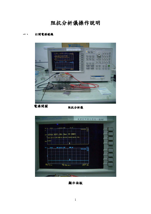
阻抗分析儀操作說明一、打開電源暖機電源開關阻抗分析儀操作面板備註:表示操作面板上既有的按鈕指令。
表示螢幕顯示按鈕上的按鈕指令。
二、校正儀器(1) 按鈕 Cal FIXTUER COMPEN OPEN 為開迴路效正,聽到BI 一聲即可 (黑、紅鱷魚夾量測頭不接觸) 。
(2) FIXTUER COMPEN SHORT 為閉迴路效正,聽到BI 即可 (黑、紅鱷魚夾量測頭接觸) 。
螢幕顯示按鈕(3) 接上量測試片設定頻率範圍,Start 為開始頻率設定,Stop 為結束頻率,初始設定為40HZ~1MHZ,最大可到110MHZ。
(4) Scale Ref AUTO SCALE 自動掃頻。
(5)Trigger HOLD自動掃頻中止SINGLE 自動掃頻一次GROUP自動掃頻依所輸入次數CONTINOUS 連續自動掃頻三、量測種類選取(1) 按鈕Meas Z-θ為阻抗量測。
(2) 按鈕Meas Cs-D 為電容及tangent loss量測。
量測以1KHZ下量測。
四、畫面顯示指令(1) 按鈕A、B 可在量測圖形或相位圖下做不同的顯現方式。
(2) 按鈕Display SPLIT ON 或OFF 為量測圖形跟相位圖是否分開顯示。
(3) 按鈕 FormatLin 或 Log為以取線性或對數顯示。
(4) 按鈕 MARKER 為移動指標到所要之位置。
可直接以數字輸入指定位置或以旋轉鈕調整。
五、等效電路量測(1) 按鈕 Display EQUIV CKT CIRCUIT ON 或 OFF 顯示電位種類。
(2) 按鈕 Display EQUIV CKT SELECT CIRCUIT (A~E)選取所要之等效電路圖。
(3) CALCULATE PARAMETERS 計算等效R1、L1、C1、C0等值。
(4) PARAMETERS ON 或OFF 為是否顯示R1、L1、C1、C0等值。
旋轉鈕數字輸入六、按鈕指令補充(1) 按鈕Marker MKR ON 或 OFFSUB MKR 可在圖形中加入其他標記CLEAR SUB MKR 清除其他標記(2) 按鈕 Utility MKR LIST ON 或 OFF(3) 按鈕 Search MAXMINPEAK NEXT PEAKNEXT PEAK LEFTNEXT PEAK RIGHT。
电阻测试仪操作流程

电阻测试仪操作流程电阻测试仪是一种用于测试电路中电阻值的仪器,广泛应用于电子、电气等相关行业。
正确的操作流程能够确保测试结果的准确性和可靠性。
本文将介绍电阻测试仪的详细操作流程。
一、准备工作1. 确保电阻测试仪处于正常工作状态,接通电源并等待其启动。
2. 验证测试仪是否进行了相关校准,根据需要进行校准操作。
3. 将测试仪的测试端子连接到待测试电路的两端,确保连接良好。
二、设置测试参数1. 在测试仪的显示屏上选择所需的测试模式,如阻值测量、连续检测等。
2. 根据需要设置测试仪的测试范围和灵敏度,以保证测试结果的准确性。
3. 确定测试仪的采样率和显示单位,如欧姆(Ω)、千欧姆(kΩ)等。
三、执行测试操作1. 确保待测电路处于断开状态,以避免干扰和电流流动。
2. 在电阻测试仪的操作界面上,按下开始测试的按钮或者选择相应的测试命令。
3. 观察测试仪的显示屏,等待测试结果的稳定显示。
4. 如果需要连续测试多个电阻值,可按下相应的扫描或持续测试功能按钮,并等待测试结果的更新。
5. 根据测试结果进行相应的记录和处理,如保存数据、计算平均值等。
四、测试结果分析1. 根据测试结果判断待测电路的电阻值是否在合理范围内,比较测试值与标准值是否相符。
2. 如果测试结果存在异常或偏差,可检查测试仪的连接是否良好,重复测试操作或进行其他排查。
3. 如果测试结果符合要求,则可以进行下一步操作或测试。
五、结束操作1. 完成测试后,关闭电阻测试仪的电源,断开与待测电路的连接。
2. 清理和维护电阻测试仪,保持其良好状态。
3. 根据需要对测试结果进行整理、分析和报告,以便后续使用和参考。
以上就是电阻测试仪的操作流程,正确的操作流程能够确保测试结果的准确性和可靠性。
在操作过程中请遵循相关安全规范,确保自身和设备的安全。
希望这篇文章能对您有所帮助!。
阻抗测量仪操作指南

阻抗测量仪操作指南引言阻抗测量仪作为一种常用的电子测试仪器,广泛应用于各个领域,包括电子工程、通信、医学和材料科学等。
它可以用来测量电路元件和材料的阻抗特性,有助于工程师和科研人员进行可靠性分析和性能评估。
本文将为大家提供一份简明扼要的阻抗测量仪操作指南,帮助读者了解如何正确使用和操作阻抗测量仪。
1. 基本原理阻抗测量仪基于交流电路理论和电压、电流测量原理。
它通过向电路中施加交流电压或电流信号,并测量电路中的电压和电流响应,从而计算得到电路的阻抗。
阻抗测量仪一般包括信号源、测量电压或电流的通道、计算器和显示器等组成部分。
2. 仪器设置在开始阻抗测量之前,首先需要正确设置仪器。
通常,仪器上会有一些旋钮和按钮,用于选择测量的参数和模式。
根据测量需求,需要选择合适的参数,如频率、信号幅度等。
此外,还需要连接合适的电缆和传感器,确保仪器与待测物之间的连通性良好。
3. 校准与校验阻抗测量仪的准确性对于测量结果的可靠性至关重要。
因此,在进行正式的测量之前,应当进行校准和校验。
校准可通过使用标准电阻和电容等校准件进行,以确认仪器的准确性。
校验则可以通过测量已知阻抗的元件或材料,验证仪器的准确性。
在校准和校验过程中,应当遵循仪器的操作手册和相关标准,确保结果的准确性和可重复性。
4. 测量步骤在进行阻抗测量时,需要按照以下步骤进行:(1) 设置合适的频率和信号幅度。
一般情况下,需要根据被测物的特性进行选择。
低频适用于测量大电容和大电感,而高频适用于测量小电容和小电感。
(2) 将被测物与仪器连接。
根据被测物的类型,选择合适的电缆和传感器,并正确连接到仪器上。
(3) 开始测量。
根据仪器的操作手册,按下开始测量的按钮或旋钮,仪器即会开始采集数据并进行计算。
(4) 分析和记录结果。
通过显示屏或输出接口,可以获得测量结果。
根据需求,可以对结果进行分析和处理,并记录在相关文件或报告中。
5. 结果解读阻抗测量仪的测量结果主要体现为电阻、电感和电容等参数。
电阻测量仪的使用方法

电阻测量仪的使用方法
电阻测量仪主要用于测量电路中元件的电阻值,以下是使用电阻测量仪的基本步骤:
1. 关闭电路:首先,需要关闭电路中的电源,确保电路处于断开状态,以防止测量过程中发生电流突变或短路。
2. 连接测量仪:将测量仪的测试笔或夹子分别连接到待测元件的两个端点上。
要确保测试笔或夹子与元件良好接触,以获得准确的测量结果。
3. 选择测量范围:根据待测元件的预估电阻范围,选择测量仪的合适量程。
如果选择过大的量程测量,可能会导致电阻值显示为溢出或无穷大。
4. 读取测量值:打开测量仪的电源开关,观察测量仪的数码显示屏或指针,记录下所测得的电阻值。
如果使用了自动测量仪,测量结果将会自动显示。
5. 断开连接:完成测量后,断开测量仪与待测元件的连接。
请注意,使用电阻测量仪时需要仔细阅读并遵守其使用说明书中的安全操作规范,以确保自身的安全和测量结果的准确性。
- 1、下载文档前请自行甄别文档内容的完整性,平台不提供额外的编辑、内容补充、找答案等附加服务。
- 2、"仅部分预览"的文档,不可在线预览部分如存在完整性等问题,可反馈申请退款(可完整预览的文档不适用该条件!)。
- 3、如文档侵犯您的权益,请联系客服反馈,我们会尽快为您处理(人工客服工作时间:9:00-18:30)。
安捷伦4395A 阻抗分析仪使用方法
1.使用频率范围:100kHz ~ 500MHz
2.使用配件(非标配):41951-69001阻抗适配器,16092弹簧夹具,0S/0Ω/50Ω校准用标准配件,同轴线缆(3条)
3.同轴线缆连接41951-69001阻抗适配器与4395A阻抗分析仪
同轴线缆4395A阻抗分析仪41951-69001阻抗适配器
NO. 1 RF OUT 50Ω端Input S端
NO. 2 R 50Ω端OUTPUT R端
NO. 3 A 50Ω或B 50Ω端OUTPUT T端
备注:连接41951-69001阻抗适配器与4395A阻抗分析仪应当在关机状态下进行。
4.测试参数设置
阻抗测试至少应当设置以下参数:
(a)测试频率范围——通过4395A阻抗分析仪前面板上的START/STOP或者CENTER/SPAN即可设置起始/终止频率或者中心频率/范围。
(b)信号输出等级——选择4395A阻抗分析仪前面板上的Source硬键,在出现的菜单中选择POWER软键可以设置信号输出等级。
参数可选范围为:-15dB ~ +15dB。
该参数与测试过程中可能出现的A或B端过载报警有关。
为避免出现报警,可以将其设置为负值。
5.校机
5.1 选择4395A前面板上的Cal硬键,在出现的软键菜单中选择CALIBRATE MENU。
5.2 开路校机。
连接0S标准配件到41951-69001阻抗适配器,选择OPEN软键。
当本操
作实施后,OPEN字样下方会出现下划线,此时可以取下0S标准配件。
5.2 短路校机。
连接0Ω标准配件到41951-69001阻抗适配器,选择SHORT软键。
当本操作实施后,SHORT字样下方会出现下划线,此时可以取下0Ω标准配件。
5.3 50Ω负载校机。
连接50Ω标准配件到41951-69001阻抗适配器,选择LOAD软键。
当本操作实施后,SHORT字样下方会出现下划线。
5.4 选择DONE CAL软键实施校机。
显示屏幕上会出现一条水平线及Cor字样,如果设置有Maker List,将会在表中显示各Maker点处的阻抗约为50Ω。
此时校机完成,可以取下50Ω标准配件。
6.安装测试夹具16092到41951-69001阻抗适配器
将测试夹具16092左端的两个定位孔正对41951-69001阻抗适配器的两个定位柱,旋转41951-69001阻抗适配器的连接头以固定夹具。
7.夹具补偿
夹具补偿是为了消除测试夹具电极与适配器输出端之间的误差,以保证测试准确性。
7.1 选择4395A阻抗分析仪前面板上的Cal硬键,在出现的屏幕菜单中选择FIXTURE COMPEN软键,在次级菜单中选择COMPEN MENU软键。
7.2 短路补偿。
松开测试夹具16092的的紧固螺旋,使两极(弹簧端)靠近,再次紧固后用短导线直接连接两极形成短路。
选择屏幕菜单中的SHORT软键。
当本操作实施后,SHORT字样下方会出现下划线。
7.3 开路补偿。
松开测试夹具16092的的紧固螺旋,使两极(弹簧端)远离形成开路,再次紧固后选择屏幕菜单中的OPEN软键。
当本操作实施后,OPEN字样下方会出现下划线。
7.4 选择DONE COMPEN软键实施校机。
显示屏幕上会出现一条水平线及Cmp字样,如果设置有Maker List,将会在表中显示各Maker点处的阻抗约为0Ω。
8.测试
8.1 选择需要测试的特性参数:
4395A阻抗分析仪可以对阻抗幅值、相位、电阻、电抗等进行测试,默认为阻抗幅值。
变更测试参数可以选择4395A阻抗分析仪前面板上的Meas硬键,再选择显示屏上对应的软键。
8.2 选择数据显示格式
4395A阻抗分析仪的数据显示格式包括线性、对数、极坐标和SMITH圆图格式。
可以通过选择前面板上的Format硬键,再在对应的屏幕菜单中选择相应的软键变更数据格式。
8.3 连接被测元件
将被测元件的两端分别连接在测试夹具16092的两极(弹簧柱)上。
8.4 自动缩放图象
为使测试曲线显示较为美观,可以选择4395A阻抗分析仪前面板上的Scale Ref硬键,在对应的屏幕菜单中选择AUTO SCALE软键自动缩放图形显示比例。
9.数据分析
可以通过对测试曲线设置Maker分析数据,选择Maker硬键,对应的屏幕菜单中选择SUB MKR,这里可以标记7个频率点,在输入需要标记的频率后选择对应的数字即可将该频率点标记。
选择4395A阻抗分析仪前面板上的Utility硬键,将MKR List软键的状态由on OFF变为ON off,此时设定好的各标记频率点将显示在屏幕下方。
选择Search硬键可以在测试曲线上定位极值、峰值点及左端或右端极值等,此时该点的测试频率和对应阻抗值将显示在图形窗口的右上角。
此功能配合SUB MKR可以较好的实现数据分析。