三安光电LED规格书-03
红光三位数LED显示器数据表说明书

Technical Data SheetTriple Digit 7-segment LED DisplaySpec No.:W5631A/B Date:16-Mar-2017Issue No.:G-001-Rev-3E-mail:*******************Features:●0.56″(inch)digit height ●Low power consumption ●High reliability●Excellent characters appearance●Available in common cathode or common anode ●RoHS CompliantDescriptions:●The KW3-567AVB/KW3-567CVB is a 0.56inch (14.20mm)height Triple digit display.●The display provides excellent reliability in bright ambient light.●Thedevice is made with white segments and black surface.Applications:●Home appliances ●Instrument panels ●Digital readout displays ●Game console systemsDevice Selection Guide:Part No.Emitting ColorPolarityKW3-567AVB Red Common Anode KW3-567CVBRedCommon CathodeTechnical Data SheetTriple Digit 7-segment LED DisplaySpec No.:W5631A/B Date:16-Mar-2017Issue No.:G-001-Rev-3E-mail:*******************Package Dimension:DIG.1DIG.2DIG.388 [0.315]2.54*5=12.7 [0.500]Notes:1.All dimensions are in millimeters (inches).2.Tolerance is ±0.25mm (.010″)unless otherwise noted.Triple Digit7-segment LED DisplayTechnical Data SheetInternal Circuit Diagram:Internal Circuit Diagram(Common Anode)KW3-567AVB1298Internal Circuit Diagram(Common Cathode)KW3-567CVB1298Spec No.:W5631A/B Date:16-Mar-2017 Issue No.:G-001-Rev-3E-mail:*******************Technical Data SheetTriple Digit 7-segment LED DisplaySpec No.:W5631A/B Date:16-Mar-2017Issue No.:G-001-Rev-3E-mail:*******************Absolute Maximum Ratings at Ta=25℃ParametersSymbolMaxUnitPower Dissipation Per Segment P d 48mW Peak Forward Current Per Segment (1/10Duty Cycle,0.1ms Pulse Width)I FP 100mA Forward Current Per Segment I F 20mA Reverse Voltage Per Segment V R 5VOperating Temperature Range T opr -40℃to +80℃Storage Temperature Range T stg -40℃to +85℃Soldering TemperatureT sld260℃for 5SecondsElectrical Optical Characteristics at Ta=25℃ParametersSymbolMin.Typ.Max.UnitTest ConditionAverage Luminous Intensity Iv 20.040.0---mcd IF=10mA (Note a)40.080.0---mcdIF=20mA (Note a)Luminous Intensity Matching Ratio I v-m ------2:1IF=10mAPeak Emission Wavelength λp ---632---nm IF=20mA Dominant Wavelength λd ---624---nm IF=20mA (Note b)Spectral Line Half-Width △λ---20---nm IF=20mA Forward Voltage Per Segment V F --- 2.0 2.4V IF=20mA Reverse Current Per SegmentI R------50µAVR=5VNotes:a.Luminous intensity is measured with a light sensor and filter combination that approximates the CIE eye-response curve.b.The dominant wavelength (λd)is derived from the CIE chromaticity diagram and represents the single wavelength which defines the color of the device.Technical Data SheetTriple Digit 7-segment LED DisplaySpec No.:W5631A/B Date:16-Mar-2017Issue No.:G-001-Rev-3E-mail:*******************Typical Electrical /Optical Characteristics Curves (25℃Ambient Temperature Unless Otherwise Noted)Spectrum DistributionR e l a t i v e L u m i n o u s I n t e n s i t y (%)Ta=25℃0400100300500600700800Wavelength λp (nm)755025Luminous Intensity &Ambient TemperatureR e l a t i v e L u m i n o u s I n t e n s i t y (%)11000-60Ambient Temperature Ta (℃)10010-40-20020406080100Luminous Intensity & Forward CurrentR e l a t i v e L u m i n o u s I n t e n s i t y (%)1100010Forward Current IF (mA)10010010*******Forward Current Derating CurveF o r w a rd C u r re n t I F (m A )010********Ambient Temperature Ta (℃)f=1KHz Duty=1/10Ta=25℃20406080100Forward Current & Forward VoltageF o r w a r d C u r r e nt I F (m A )Ta=25℃010*********.41.6 1.82.0 2.2 2.4Forward Voltage VF (V)2.6Technical Data SheetTriple Digit 7-segment LED DisplaySpec No.:W5631A/B Date:16-Mar-2017Issue No.:G-001-Rev-3E-mail:*******************Packing &LabelSpecifications:LabelOutside BoxDateSidePearl WoolInner BoxTriple Digit7-segment LED DisplayTechnical Data SheetTerms and conditions for the usage of this document:a.The information included in this document reflects representative usage scenarios and is intended for technicalreference only.b.The part number,type,and specifications mentioned in this document are subject to future change andimprovement without notice.Before production usage customer should refer to the latest datasheet for theupdated specifications.c.When using the products referenced in this document,please make sure the product is being operated within theenvironmental and electrical limits specified in the datasheet.If customer usage exceeds the specified limits, Luckylight will not be responsible for any subsequent issues.d.The information in this document applies to typical usage in consumer electronics applications.If customer'sapplication has special reliability requirements or have life-threatening liabilities,such as automotive or medical usage,please consult with Luckylight representative for further assistance.e.The contents and information of this document may not be reproduced or re-transmitted without permission byLuckylight.f.Over-current-proofCustomer must apply resistors for protection,otherwise slight voltage shift will cause big current change(Burn out will happen).g.Storage1.Before opening the package,the LEDs should be kept at30℃or less and80%RH or less.2.The LEDs should be used within a year.3.After opening the package,the LEDs should be kept at30℃or less and60%RH or less.Spec No.:W5631A/B Date:16-Mar-2017Issue No.:G-001-Rev-3E-mail:*******************Technical Data SheetTriple Digit 7-segment LED DisplaySpec No.:W5631A/B Date:16-Mar-2017Issue No.:G-001-Rev-3E-mail:*******************Through Hole Display Mounting MethodLead Forming:1.Do not bend the component leads by hand without proper tools.2.The leads should be bent by clinching the upper part of the lead firmly such that the bending force Is not exerted on the plasticbody.Installation:1.The installation process should not apply stress to the lead terminals.2.When inserting for assembly,ensure the terminal pitch matches the substrate board’s hole pitch to prevent spreading or pinching the leadterminals.Not Recommended Recommended3.The component shall be placed at least 5mm from edge of PCB to avoid damage caused excessive heat during wavesoldering.Technical Data SheetTriple Digit 7-segment LED DisplaySpec No.:W5631A/B Date:16-Mar-2017Issue No.:G-001-Rev-3E-mail:*******************R e c o m m e n d e d W a v e S o ld e rin g P ro file sT e m p e r a t u r e(℃)T im e (s e c)50100150200250300Notes:1.Recommend pre-heat temperature of 105℃or less (as measured with a thermocouple attached to the LED pins)prior to immersion in the solder wave with a maximum solder bath temperature of 260℃.2.Peak wave soldering temperature between 245℃~255℃for 3sec (5sec max).3.Do not apply stress to the epoxy resin while the temperature is above 85℃.4.Fixtures should not incur stress on the component when mounting and during soldering process.5.SAC 305solder alloy is recommended.6.No more than one wave soldering pass.7.During wave soldering,the PCB top-surface temperature should be kept below 105℃.Soldering General Notes:1.Through-hole displays are incompatible with reflow soldering.2.If components will undergo multiple soldering processes,or other processes where the omponents may be subjected to intense heat,please check with luckylight for compatibility.Technical Data SheetTriple Digit 7-segment LED DisplaySpec No.:W5631A/B Date:16-Mar-2017Issue No.:G-001-Rev-3E-mail:*******************Cleaning:d “no-clean”fluxes are recommended for use in soldering.2.If cleaning is required,luckylight recommends to wash components with water only.Do not use harsh organic solvents for cleaning because they may damage the plastic parts.3.The cleaning process should take place at room temperature and the devices should not be washed for more than one minute.4.When water is used in the cleaning process,immediately remove excess moisture from the component with forced-air drying afterwards.Circuit Design Notes:1.Protective current-limiting resistors may be necessary to operate the LEDs within the specified range.2.LEDs mounted in parallel should each be placed in series with its own current-limitingresistor.Recommended Set-up Invalid Set-upGND VSVSGND3.The driving circuit should be designed to protect the LED against reverse voltages and transient voltage spikes when the circuit is powered up or shut down.4.The safe operating current should be chosen after considering the maximum ambient temperature of the operating environment.5.Prolonged reverse bias should be avoided,as it could cause metal migration,leading to an increase in leakage current or causing a short circuit.。
Wheelock Exceder LED3系列产品说明书

MOUNTING OPTIONS
1. Connect field wiring to contacts on back of device. 2. Dress wires back into backbox. 3. Install device as shown in Figure 4,Figure 5, or Figure 6 (4” square backbox or octal) with the screws provided. 4. Snap beauty cover over device.
GENERAL
The Wheelock Exceder LSTC3-B strobe appliances are designed for easy installation. All models are for 24V operation. LSTC3-B is designed for ceiling mounting only.
WARNING: Please read these instructions carefully before using this product. Failure to comply with any of the following instructions, cautions and warnings could result in improper application, candela setting, installation and/or operation of these products in an emergency situation, which could result in property damage and serious injury or death to you and/or others.
三安光电推出四款高端LED芯片

三安光电推出四款高端LED芯片
【字体:大中小简繁】【收藏】【关闭】
三安光电20日在深圳召开
新品推介会,推出四款高端LED
芯片新品。
业内人士评价,四款
产品在技术上具备国内领先、国
际先进的优势,市场应用价值和
推广度很高,为公司进一步做大
LED芯片产业,跻身国际知名
LED芯片生产企业再添重要筹
码。
据了解,三安此次推出的四
款新品,一是GaN基发光二极
管大功率芯片,该新品的研制成功,使公司成为国内唯一一家拥有自主知识产权、从外延到芯片可批量生产的企业,此新品封装成白灯单灯可达120lm,效率为100lm/W以上,高于国家路灯80lm/W的要求,产品已通过相关路灯实验;二是GaN基发光二极管超亮(白光)芯片,该新品封装成白灯功率可达到110lm/W,可广泛用于平板电视、笔记本电脑等显示器背光源、半导体照明等高端领域;三是GaAs超高亮发光二极管红光芯片,该产品主要用于户外显示屏、汽车尾灯、照明等领域,其封装后的光功率可达到60lm/W;四是GaAs超高亮发光二极管黄绿芯片,该产品的裸晶在80mcd左右,主要用于双色显示屏,LCD背光源等领域。
有业内人士认为,三安此次推出的四款新品应用领域广泛,尤其是在我国城市亮化美化工程和大力发展汽车工业等背景下,市场空间巨大;同时,这些新品的上市,也极大地支持了国内LED行业的发展和产业链条的有效形成,为国内下游企业度过金融危机的冲击提供了技术、产品和成本上的保证,有效地促进了国内LED行业的发展。
公司表示,伴随着天津三安的组建和陆续投产,2010年公司一期扩产后将完成年产LED外延片150万片,芯片350亿粒的产能规模,并计划于2012年底前完成100台MOCVD 的扩产任务,实现行业全球前五名的目标。
三安光电灯珠 规格书

三安光电灯珠规格书
三安光电是一家专业从事LED照明产品研发、生产和销售的公司,其灯珠产品规格书通常包括以下内容:
1. 产品概述,规格书通常会首先介绍该款灯珠的产品概述,包
括产品系列、型号、用途等基本信息。
2. 光电参数,这部分会详细列出灯珠的光电参数,如发光功率、光通量、发光角度、色温、色坐标等,以及光电性能曲线图表。
3. 尺寸和外观,规格书会描述灯珠的尺寸、外形结构、引线配
置等详细信息,以便用户了解产品的实际尺寸和外观特征。
4. 电气参数,包括额定电流、正向电压、反向电压等电气参数
的具体数值,以及电气性能曲线图表。
5. 热学参数,描述灯珠的工作温度范围、热阻、热传导性能等
热学参数,以及与热管理相关的建议和注意事项。
6. 包装信息,规格书通常也会包括产品的包装规格、包装方式、
存储条件等信息,以便用户在购买和使用时参考。
7. 安装和使用说明,针对灯珠的安装方法、使用注意事项、典型应用场景等进行详细说明,帮助用户正确使用产品。
8. 质量保证,描述产品的质量保证体系、质量标准、测试方法等内容,让用户了解产品的质量保证情况。
以上是一般情况下三安光电灯珠规格书中可能包含的内容,具体规格书内容可能会因产品型号、系列、用途等而有所差异。
希望以上信息能够帮助到你。
红外LED产品说明书.pdf_1718622854.050958
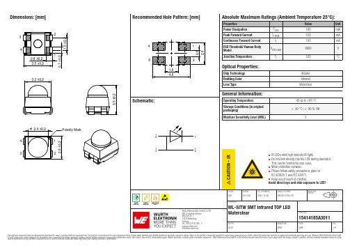
Dimensions: [mm]344315414185A301115414185A301115414185A301115414185A3011BC15414185A3011T e m p e r a t u r eT pT L15414185A3011Cautions and Warnings:The following conditions apply to all goods within the product series of Optoelectronic Components of Würth Elektronik eiSos GmbH & Co. KG:General:•This optoelectronic component is designed and manufactured for use in general electronic equipment.•Würth Elektronik must be asked for written approval (following the PPAP procedure) before incorporating the components into any equipment in fields such as military, aerospace, aviation, nuclear control, submarine, transportation (automotive control, train control, ship control), transportation signal, disaster prevention, medical, public information network, etc. where higher safety and reliability are especially required and/or if there is the possibility of direct damage or human injury.•Optoelectronic components that will be used in safety-critical or high-reliability applications, should be pre-evaluated by the customer. •The optoelectronic component is designed and manufactured to be used within the datasheet specified values. If the usage and operation conditions specified in the datasheet are not met, the wire insulation may be damaged or dissolved.•Do not drop or impact the components, the component may be damaged.•Würth Elektronik products are qualified according to international standards, which are listed in each product reliability report. Würth Elektronik does not warrant any customer qualified product characteristics beyond Würth Elektroniks’ specifications, for its validity and sustainability over time.•The responsibility for the applicability of the customer specific products and use in a particular customer design is always within the authority of the customer. All technical specifications for standard products also apply to customer specific products.•Unless Würth Elektroik has given its express consent, the customer is under no circumstances entitled to reverse engineer, disassemble or otherwise attempt to extract knowledge or design information from the optoelectronic component.Product specific:Soldering:•The solder profile must comply with the technical product specifications. All other profiles will void the warranty.•All other soldering methods are at the customers’ own risk.•The soldering pad pattern shown above is a general recommendation for the easy assembly of optoelectronic component. If a high degree of precision is required for the selected application (i.e. high density assembly), the customer must ensure that the soldering pad pattern is optimized accordingly.Cleaning and Washing:•Washing agents used during the production to clean the customer application might damage or change the characteristics of the optoelectronic component body, marking or plating. Washing agents may have a negative effect on the long-term functionality of the product. •Using a brush during the cleaning process may break the optoelectronic component body. Therefore, we do not recommend using a brush during the PCB cleaning process.Potting:•If the product is potted in the customer application, the potting material might shrink or expand during and after hardening. Shrinking could lead to an incomplete seal, allowing contaminants into the optoelectronic component body, pins or termination. Expansion could damage the components. We recommend a manual inspection after potting to avoid these effects.Storage Conditions:• A storage of Würth Elektronik products for longer than 12 months is not recommended. Within other effects, the terminals may suffer degradation, resulting in bad solderability. Therefore, all products shall be used within the period of 12 months based on the day of shipment.•Do not expose the optoelectronic component to direct sunlight.•The storage conditions in the original packaging are defined according to DIN EN 61760-2.•For a moisture sensitive component, the storage condition in the original packaging is defined according to IPC/JEDEC-J-STD-033. It is also recommended to return the optoelectronic component to the original moisture proof bag and reseal the moisture proof bag again. •The storage conditions stated in the original packaging apply to the storage time and not to the transportation time of the components. Packaging:•The packaging specifications apply only to purchase orders comprising whole packaging units. If the ordered quantity exceeds or is lower than the specified packaging unit, packaging in accordance with the packaging specifications cannot be ensured. Handling:•Violation of the technical product specifications such as exceeding the nominal rated current, will void the warranty.•The product design may influence the automatic optical inspection.•Certain optoelectronic component surfaces consist of soft material. Pressure on the top surface has to be handled carefully to prevent negative influence to the function and reliability of the optoelectronic components.•ESD prevention methods need to be applied for manual handling and processing by machinery.•Resistors for protection are obligatory.•Luminaires in operation may harm human vision or skin on a photo-biological level. Therefore direct light impact shall be avoided. •In addition to optoelectronic components testing, products incorporating these devices have to comply with the safety precautions given in IEC 60825-1, IEC 62471 and IEC 62778.•Please be aware that Products provided in bulk packaging may get bent and might lead to derivations from the mechanicalmanufacturing tolerances mentioned in our datasheet, which is not considered to be a material defect.Würth Elektronik eiSos GmbH & Co. KGEMC & Inductive SolutionsMax-Eyth-Str. 174638 WaldenburgGermanyCHECKED REVISION DATE (YYYY-MM-DD)GENERAL TOLERANCE PROJECTIONMETHODZAn001.0002021-10-26DIN ISO 2768-1mDESCRIPTIONWL-SITW SMT Infrared TOP LEDWaterclear ORDER CODE15414185A3011SIZE/TYPE BUSINESS UNIT STATUS PAGETechnical specification:•The typical and/or calculated values and graphics of technical parameters can only reflect statistical figures. The actual parameters of each single product, may differ from the typical and/or calculated values or the typical characteristic line.•On each reel, only one bin is sorted and taped. The bin is defined on intensity, chromaticity coordinate or wavelength and forward voltage.•In order to ensure highest availability, the reel binning of standard deliveries can vary. A single bin cannot be ordered. Please contact us in advance, if you need a particular bin sorting before placing your order.•Test conditions are measured at the typical current with pulse duration < 30ms. •Optical properties are measured according the CIE 127:2007 standard.•Wavelength tolerance under measurement conditions ± 2nm.•Optical intensity tolerance under measurement conditions ±15%.•Forward voltage tolerance under measurement conditions ± 0.1V.•CCT tolerance of x and y coordinate of ± 0.01and CRI tolerance of ± 2 is allowed In the characteristics curves, all values given in dotted lines may show a higher deviation than the parameters mentioned above.These cautions and warnings comply with the state of the scientific and technical knowledge and are believed to be accurate and reliable.However, no responsibility is assumed for inaccuracies or incompleteness.The customer has the sole responsibility to ensure that he uses the latest version of this datasheet, which is available on Würth Elektronik’s homepage. Unless otherwise agreed in writing (i.e. customer specific specification), changes to the content of this datasheet may occurwithout notice, provided that the changes do not have a significant effect on the usability of the optoelectronic componentsWürth Elektronik eiSos GmbH & Co. KG EMC & Inductive Solutions Max-Eyth-Str. 174638 Waldenburg GermanyCHECKED REVISION DATE (YYYY-MM-DD)GENERAL TOLERANCEPROJECTION METHODZAn001.0002021-10-26DIN ISO 2768-1mDESCRIPTIONWL-SITW SMT Infrared TOP LED WaterclearORDER CODE15414185A3011SIZE/TYPEBUSINESS UNITSTATUSPAGEImportant NotesThe following conditions apply to all goods within the product range of Würth Elektronik eiSos GmbH & Co. KG:1. General Customer ResponsibilitySome goods within the product range of Würth Elektronik eiSos GmbH & Co. KG contain statements regarding general suitability for certain application areas. These statements about suitability are based on our knowledge and experience of typical requirements concerning the areas, serve as general guidance and cannot be estimated as binding statements about the suitability for a customer application. The responsibility for the applicability and use in a particular customer design is always solely within the authority of the customer. Due to this fact it is up to the customer to evaluate, where appropriate to investigate and decide whether the device with the specific product characteristics described in the product specification is valid and suitable for the respective customer application or not.2. Customer Responsibility related to Specific, in particular Safety-Relevant ApplicationsIt has to be clearly pointed out that the possibility of a malfunction of electronic components or failure before the end of the usual lifetime cannot be completely eliminated in the current state of the art, even if the products are operated within the range of the specifications.In certain customer applications requiring a very high level of safety and especially in customer applications in which the malfunction or failure of an electronic component could endanger human life or health it must be ensured by most advanced technological aid of suitable design of the customer application that no injury or damage is caused to third parties in the event of malfunction or failure of an electronic component. Therefore, customer is cautioned to verify that data sheets are current before placing orders. The current data sheets can be downloaded at .3. Best Care and AttentionAny product-specific notes, cautions and warnings must be strictly observed. Any disregard will result in the loss of warranty.4. Customer Support for Product SpecificationsSome products within the product range may contain substances which are subject to restrictions in certain jurisdictions in order to serve specific technical requirements. Necessary information is available on request. In this case the field sales engineer or the internal sales person in charge should be contacted who will be happy to support in this matter.5. Product R&DDue to constant product improvement product specifications may change from time to time. As a standard reporting procedure of the Product Change Notification (PCN) according to the JEDEC-Standard inform about minor and major changes. In case of further queries regarding the PCN, the field sales engineer or the internal sales person in charge should be contacted. The basic responsibility of the customer as per Section 1 and 2 remains unaffected.6. Product Life CycleDue to technical progress and economical evaluation we also reserve the right to discontinue production and delivery of products. As a standard reporting procedure of the Product Termination Notification (PTN) according to the JEDEC-Standard we will inform at an early stage about inevitable product discontinuance. According to this we cannot guarantee that all products within our product range will always be available. Therefore it needs to be verified with the field sales engineer or the internal sales person in charge about the current product availability expectancy before or when the product for application design-in disposal is considered. The approach named above does not apply in the case of individual agreements deviating from the foregoing for customer-specific products.7. Property RightsAll the rights for contractual products produced by Würth Elektronik eiSos GmbH & Co. KG on the basis of ideas, development contracts as well as models or templates that are subject to copyright, patent or commercial protection supplied to the customer will remain with Würth Elektronik eiSos GmbH & Co. KG. Würth Elektronik eiSos GmbH & Co. KG does not warrant or represent that any license, either expressed or implied, is granted under any patent right, copyright, mask work right, or other intellectual property right relating to any combination, application, or process in which Würth Elektronik eiSos GmbH & Co. KG components or services are used.8. General Terms and ConditionsUnless otherwise agreed in individual contracts, all orders are subject to the current version of the “General Terms and Conditions of Würth Elektronik eiSos Group”, last version available at .Würth Elektronik eiSos GmbH & Co. KGEMC & Inductive SolutionsMax-Eyth-Str. 174638 WaldenburgGermanyCHECKED REVISION DATE (YYYY-MM-DD)GENERAL TOLERANCE PROJECTIONMETHODZAn001.0002021-10-26DIN ISO 2768-1mDESCRIPTIONWL-SITW SMT Infrared TOP LEDWaterclear ORDER CODE15414185A3011SIZE/TYPE BUSINESS UNIT STATUS PAGE。
INL-03XLED灯应急电源规格书

7.3、测试开关
开关状态
功能
模式
按下<3 秒
模拟断电测试
按下 3-5 秒
模拟自检/月检功能①
主电
按下>5 秒
模拟自检/年检功能①
按下<6 秒 按下>6 秒
关闭/打开应急输出② 彻底关闭应急输出③
电池
注①:模拟月/年检状态下,再次按下测试开关,取消模拟自检功能。月检/年检状态下无效。
注②:(手动应急控制)须电池组有正常的电量和市电触发后有效。
INC-032 86010032 LED 灯具
40-80 220~AC 50/60 Max 6 11.1/12
-25 45 70 -25—70
Data 13/07/14 INC-03X_SPEC V1.1_CN 如有更改恕不另行通知
2/5
5.2、电池尺寸(A2 型 / 连接线长:150-170 mm)
INL-03X LED 灯应急电源规格书
六、安装布线 6.1、接线图
N L
LED灯具
照明开关
OUT
OUT
N
L1
INC-03X
L
Bat Bat + LED/K LED/A Switch Switch
12V电池组 LED指示灯 测试开关
6.2、连接线类型及截面积 使用单芯线或多股绞合线,截面 0.75mm²-1.5mm²的铜芯线布线。线端剥 开 6-8mm 的裸线(右图),确保完好的接入本控制装置的接线端子并压紧。 6.3、布线注意事项 功率 LED 的连接线会增加损耗应尽量短些,推荐灯的连线使用小于 3 米的铜芯线连接。指示灯及测试按钮 的连线应小于 1 米。墙壁照明开关(L 和 L1 之间),其布线时须在同一相线上,布线距离应小于 100 米。推 荐使用小于 50 米的铜芯线连接。为安全的使用本控制装置及避免损坏本控制装置,请勿将两路相线接入本 控制器。LED 光源为有极性光源,请勿将极性接错,以免导致故障及额外的损失。为正确安全的使用本控 制装置,请严格按照接线图正确接线(见 6.1 节)。 6.4、安装推荐 本产品拥有良好的热处理单元,为保证产品性能、可靠性及使用寿命,应使本产品拥有良好的散热条件及使 用环境。为确保良好的散热,应使本产品的底部良好的安装在金属板上或远离发热源,使本产品工作环境温 度控制在允许的范围内。 6.5、电磁干扰 ● 不要将电源输入线和灯连接线交叉布线。 ● 尽量不要将电源输入线和灯连接线长距离平行布线,平行布线时应留 5-10cm 的距离。 ● 不要将电源输入线太贴近本控制装置。 ● 弯曲灯连接线。 ● 缩短电源输入线到本控制装置的连线距离。 ● 并联多个运行时应使电源输入线和灯的连接线尽可能短。
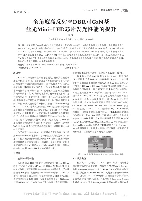
全角度高反射率DBR对GaN基蓝光Mini-LED芯片发光性能的提升
中国新技术新产品2021 NO.10(下)高 新 技 术0 引言Mini-LED背光显示技术具有色域宽、亮度高以及饱和度高等优点,在电视、显示器以及平板电脑等消费类电子产品领域具有广阔的应用前景和巨大的市场价值[1-2],也是近年来全球LED领域的研究热点[3]。
GaN基Mini-LED芯片通常采用倒装结构,早期倒装LED芯片采用金属Ag反射镜提高光萃取效率[4-9],A g薄膜电阻率低,有利于电流扩展,适合大功率芯片,主要用于车灯市场。
不过Ag容易氧化和迁移,芯片在老化过程中经常出现漏电流。
为了提高倒装芯片的可靠性,研究人员用分布布拉格反射镜(Distributed Bragg Reflector,DBR)替代Ag反射镜。
DBR是由高低折射率介质材料周期性交替组成的光学膜系,介质材料具有较高的稳定性,采用DBR作为反射镜可以提高器件的良率和可靠性[10]。
传统DBR膜系中每层材料厚度对应中心波长的1/4,对正入射的光具有高反射率,随着入射角度变大,DBR膜系反射谱会出现反射率急剧下降的现象,这种变化会限制GaN基Mini-LED芯片光萃取效率的提升,进而降低了芯片的发光效率。
为了提高GaN基Mini-LED芯片的光萃取效率,该文采用Essential Macleod软件设计了一种全角度高反射率DBR膜系,并使用光学镀膜机制备该新型DBR膜系,角度分辨反射谱测量结果与模拟值吻合。
笔者进一步验证发现,采用全角度高反射率DBR膜系与传统结构DBR膜系相比,能够有效提升GaN基Mini-LED芯片的光输出功率。
1 实验1.1 模拟和样品制备GaN基Mini-LED芯片的电致发光谱在420 nm~480 nm 波段,中心波长大约为445 nm。
根据GaN基Mini-LED芯片的发光波段,该实验采用Essential Macleod软件设计了一种新型的DBR膜系,该膜系在420 nm~480 nm波段、 0°~90 °入射角下具有较高的反射率。
3030RGB红绿蓝黄橙紫贴片灯珠规格书
3030RGB红绿蓝黄橙紫贴片灯珠规格书3030RGB red green blue SMD beads Specifications
描述Description
3030RGB在于性能稳定,性价比高.市面上用03030RGB灯珠主要用于亮化灯具,室内灯具广告
3030RGB支架同时可以做成红、绿、蓝、黄、橙、紫等单色光及白色复合光
1.产品具有亮度高,寿命长的优点,6000小时0光衰
2.该产品采用铜支架, 金线(99.999%)进行生产,质量有保证
3.我司从订单到发货最快1天内出货,无现货或定制产品,6个工作日内发货.
CUSTOMER SIGNATURE:
(Units : mm)
静电 Static Electricity
触摸 LED 时,推荐使用防静电手腕带或防静电手套.
It is recommended that a wrist band or an anti-electrostatic glove be used when handling the LEDs.
所有装置、设备、机器均应接地.
All devices, equipment and machinery must be properly grounded.
正向电压变低或在低电流时死灯.标准: IF=0.5mA 时, VF >
2.0V Damaged LEDs will show some unusual characteristics such as the forward voltage becomes
lower, or the LEDs do not light at the low current. Criteria : (VF > 2.0V at IF=0.5mA)。
- 1、下载文档前请自行甄别文档内容的完整性,平台不提供额外的编辑、内容补充、找答案等附加服务。
- 2、"仅部分预览"的文档,不可在线预览部分如存在完整性等问题,可反馈申请退款(可完整预览的文档不适用该条件!)。
- 3、如文档侵犯您的权益,请联系客服反馈,我们会尽快为您处理(人工客服工作时间:9:00-18:30)。
2011E1
S-08R *DUX - GaN
◆ 产品特点:
● 高亮度、长寿命 ● 户内外应用 ● 芯片百分百测试分选 ● 波长和光强良好一致性 ◆ 物理参数:
◆ 光电参数:(Tc=22℃, I F =20mA)
◆ 其它说明
● 光电参数均系三安光电测试仪器在晶圆条件下样测试 ● 芯片封装工艺最高温度低于280℃,持续时间小于10秒 ● GaN LED 芯片为静电敏感产品,使用、运输时注意静电防护 ● 主波长测量误差±1.0nm
● 可根据客户需要订做特殊规格的芯片
产品型号
波长均值范围
( WLD ,nm )
正向电压均值范围
( V F ,V ) 光强均值范围 (I V ,mcd )
S-08ABAU * 450~475
3.0~3.6
30~100
P 电极 金 N 电极 金
芯片尺寸 8.0mil × 7.0mil (203±15μm × 178±15μm)
芯片厚度 3.1mil (80±15μm)
焊盘尺寸
3.0mil (75±10μm) in diameter
S-08ABAU *
GaN 3.1。