AXP288 SCH Design Guide
阿里斯塔 MXP 光纤技术指南说明书

ARISTA PORTFOLIO WITH MXP PORTSArista offers a portfolio of leaf and spine switches with MXP ports for high-density applications. Arista platforms with MXP ports range from the flagship 7500E spine switch series to ultra deep buffer top of rack 7280E and the high performance 7050X top of rack switches. The MXP ports offer flexibility to customers with investment protection when migrating from 10G to 40G and 100G speeds while maintaining low cost/bit and high reliability.Table 1: Arista Switch Portfolio with MXP portsSwitch FamilyPart Number# of MXPsSupported Speeds7500E7500E-12CM 12 10/40/100G 7500E-72S 2 10/40/100G 7280E 7280SE-72 2 10/40/100G 7050X7050SX-72 2 10/40G 7050SX-96 4 10/40G7050TX-72 2 10/40G 7050TX-96410/40GIntroduction:The MXP ports on Arista leaf and spine switches can run as standards based 10Gb, 40Gb or 100Gb Ethernet, and simply require the correct fiber cables to enable multi-vendor interoperability. This technical guide is intended to provide accurate information for cabling triple-speed MXP ports with MTP and MPO cables for use with the Arista 7500E and 7280E (10GbE, 40GbE and 100GbE ports) and Arista 7050X (10GbE and 40GbE ports).MTP andMPO cablesarewidely availableand this guide provides theinformation neededto specify cables to connect to the MXP interface. Arista customers should provide this document to their cabling vendors to get cables for their specific needs.The Arista 7500E Series deliver line rate non-blocking switching that enables faster and simpler network designs. The 7500E Series offers two choices for the datacenter a 4-slot 7504 and the 8-slot 7508. The 7500E Series supports a range of interface speeds from 100Mbps up to 100Gbps Ethernet in a single system, ensuring broad choices without limiting system performance when scaling from 10Gb to 100Gb Ethernet.The 7508E is a 11RU chassis with a 30Tbps fabric that supports up to 8 line cards and provides 1,152 – 10Gb ports, 288 – 40Gb ports, or 96 – 100Gb Ethernet ports in a single system - unparalleled density and performance in the industry.The Arista 7504E provides room for 4 line cards in a compact 7RU chassis that delivers 15Tbps of bandwidth allowing up to 576 - 10Gb ports, 144 – 40Gb ports, and a massive 48 – 100Gb Ethernet ports.A choice of high-density wire-speed 10GbE, 40GbE and 100GbE line cards is fully supported with the ability to mix and match any combination of modules. The 40GbE and 100GbE modules enable up to 144x10G ports per line card. Each 40G interface can be used as either a single 40G port or quad 10G Ethernet ports. The 100G MXP interfaces can be a single port of 100Gb, three ports of 40Gb or 12 ports of 10Gb Ethernet.Figure 1: 7504E and 7508E with up to 1,152 10G portsThe Arista 7500E Series offers additional line card choices for 100GbE that are based on pluggable Optical transceivers and offer a range of reaches and media types.The 7500E-6C2-LC has 6 ports using CFP2 that can be used with a range of pluggable transceivers. The extended reach capabilities of a CFP2 form factor makes it an attractive choice for customers that need up to 40km of link distance in addition to single mode and multi-mode combinations.The 7500E-12CQ-LC has 12 ports of QSFP100 that can be used with both 100GbE and 40GbE QSFP pluggable transceivers. QSFP100 allows for a range of high-density 100G solutions due to the small size and low power. It supports a full range of industry standard interfaces with both multi-mode and single-mode fiber as well as copper cables.ARISTA 7280EThe Arista 7280E Series are purpose-built 10/40/100GbE ultra deep buffer fixed configuration systems built for the highest performance environments, where wire speed L2 and L3 forwarding are combined with advanced features for network virtualization, open monitoring and network analysis, resiliency and architectural flexibility.The 7280E Series are available in three models each with 48 SFP+ ports for 1/10GbE and choice of 40GbE and 100GbE uplinks. The 7280SE-72 has two 100GbE uplinks through the use of Arista MXP interfaces and embedded optics. Each MXP port enables twelve 10GbE, three 40GbE or one 100GbE for a wide choice of cost effective connections. The 7280SE-64 has four QSFP+ uplink ports that allow a choice of four 40GbE or up to 16 additional 10GbE ports with a range of transceivers or cables. The 7280SE-68 has two 100GbE QSFP uplinks that allow the use of both 100GbE and 40GbE optics for the widest range of both short and long reach connection optics.The Arista 7050X Series are purpose-built 10/40GbE switches with wire speed layer 2/3/4 performance combined with low latency and advanced features for software defined cloud networking.•The 7050SX-72 and 7050SX-96 provide a 1RU system with 48 10GbE SFP+ ports and 2 or 4 MXP ports that each support 3x40GbE or 12x10GbE.•The 7050TX-72 and 7050TX-96 provide a 1RU system with 48 10GBASE-T ports and 2 or 4 MXP ports that each support 3x40GbE or 12x10GbE.DEPLOYING AN OPTICAL CABLING INFRASTRUCTURE IN THE DATA CENTER FOR 40G AND 100GRecommended cabling infrastructure deployments in the data center are based upon guidance found in TIA-942, “Telecommunications Infrastructure Standard for Data Centers.” Utilizing a distributed star topology in a structured cabling implementation provides the most flexible and manageable infrastructure. Many data center deployments today utilize the reduced topology described in TIA-942, where the Horizontal Distribution Areas (HDAs) shown are collapsed to the Main Distribution Area (MDA). In this collapsed architecture, the cabling is installed between the MDA and the Equipment Distribution Areas (Figure 2).Figure 2: TIA 942 ArchitectureFor optimized performance in meeting data center requirements, the topology of the cabling infrastructure should not be selected alone; infrastructure topology and product solutions must be considered in unison.Cabling deployed in the data center today to support 10GbE must be selected to support data rate applications of the future, such as 40Gb and 100Gb Ethernet. To do this, OM3 or OM4 multi-mode fiber is a must as the legacy OM1 and OM2 specifications do not support either 40GbE or 100GbE. In addition to being the only multimode fibers included in the 40G and 100G Ethernet standard, OM3 and OM4 fibers provide the highest performance as well as the extended reach often required for structured cabling installations in the data center.In addition to the performance requirements the choice in physical connectivity is also important. Because parallel optics technology requires data transmission across multiple fibers simultaneously, a multi-fiber (or array) connector is required. Utilizing MPO-based connectivity in today’s installations for either 10G or 40G Ethernet provides the means to migrate to this multi-fiber parallel optic interface when needed.Factory-terminated MPO solutions allow connectivity to be achieved through a simple plug-and-play system. To meet the needs of today’s serial Ethernet applications, MPO- terminated backbone/horizontal cabling is simply installed into pre-terminated modules, panels or harnesses (Figure 3).Figure 3: Pre-terminated Solutions (courtesy of Corning Cable Systems)CABLING ARISTA MXP PORTS WITH MTP CABLESTraditional optical-based Ethernet physical media (for speeds below 10Gb) required a duplex fiber scheme and required only two fibers for transmit and receive. The IEEE “SR” specifications for 40Gbps and higher multimode cabling uses parallel optics. By combining multiple channels, each running at 10Gbps or 25Gbps the higher data rates are achieved. This parallel transmission approach requires the use of parallel fiber cables for both structured and non-structured systems. Structured cabling systems use MTP-12 and MTP-24 as standard cabling options. The 40GBASE-SR4 and 100GBASE-SR4 specifications require 4 pairs (8 fibers) in a 12-fiber cable, and the 100GBASE-SR10 standard requires 10 pairs (20 fibers) in a 24-fiber cable.Figure 4: MTP-12 and MTP-24 Connectors (courtesy of Complete Connect)As the 40GbE SR4 specification only uses 8 of the 12 pins in the MTP-12 connector 4 are left unused (or not present). This need for just 8 fibers out of 12 allows an MTP-24 to be used to transport three 40GbE links each utilizing 8 fibers. This is used in structured cabling systems to optimize the trunk utilization between cabling distribution points.Each 40GbE connection is presented to the active equipment as an MTP-12 connector but with only 8f present, which maximizes the channel capacity.The Arista MXP ports provide an MTP-24 port, which can be operated in one of many modes: 1 port of 100GbE, 3 ports of 40GbE or 12 ports of 10GbE and combinations of 10GbE and 40GbE. Each mode uses the same MTP-24 port, and a series of breakout cables is used to adapt this to the correct number of terminations.For example, a 24 fiber MTP to 3x 8-fiber MTP-12 can be used to provide 3 40GbE ports. Figure 5 below shows an example of the cable.Figure 5: 24-fiber MTP to 3x 8-fiber MTP (image courtesy of Leviton Network Solutions)QSFP Port 2QSFP Port 3Fiber 24 RX11Fiber 12 TX11Fiber 1 TX0Fiber 13 RX0QSFP Port 1Receptacles PlugsFiber 1-4TXFiber 9-12 RXFigure 6: MTP-24 pin-outDual LC 1ToDual LC12(12 pairs) Figure 8: MTP-24 to 12x LC break out cableTable 4: MTP-24 to 12 LC Point to Point (Cross-over) cable1 TX 1/B 13 RX 1/A2 TX 2/B 14 RX 2/A3 TX 3/B 15 RX 3/A4 TX 4/B 16 RX 4/A5 TX 5/B 17 RX 5/A6 TX 6/B 18 RX 6/A7 TX 7/B 19 RX 7/A8 TX 8/B 20 RX 8/A9 TX 9/B 21 RX 9/A10 TX 10/B 22 RX 10/A11 TX 11/B 23 RX 11/A12 TX 12/B 24 RX 12/ASUMMARYMXP ports enable high density and flexible connectivity options. Each of the MXP modes requires the use of the correct breakout cable to adapt the MTP-24 interface to either 100GbE, 40GbE or 10GbE presentation. The cable specifications shown in this document provide the information on how to identify the correct cable types. In addition cables that are pre-defined for usage with Arista MXP in each of the modes described are available directly from Arista Networks in both 3m and 5m lengths.Santa Clara—Corporate Headquarters 5453 Great America Parkway Santa Clara, CA 95054 Tel: 408-547-5500 San Francisco —R&D and Sales Office 1390 Market Street Suite 800 San Francisco, CA 94102India —R&D Office Eastland Citadel102, 2nd Floor, Hosur Road Madiwala Check Post Bangalore - 560 095Vancouver —R&D OfficeSuite 350, 3605 Gilmore Way Burnaby, British Columbia Canada V5G 4X5Ireland —International Headquarters Hartnett Enterprise Acceleration Centre Moylish Park Limerick, IrelandSingapore —APAC Administrative Office 9 Temasek Boulevard#29-01, Suntec Tower Two Singapore 038989Copyright © 2013 Arista Networks, Inc. All rights reserved. CloudVision, Extensible Operating System, and EOS are registered trademarks and Arista Networks is a ABOUT ARISTA NETWORKSArista Networks was founded to deliver software-defined cloud networkingsolutions for large data center and computing environments. The award-winning Arista 10 Gigabit Ethernet switches redefine scalability, robustness, and price-performance. More than one million cloud networking ports are deployedworldwide. The core of the Arista platform is the Extensible Operating System (EOS ®), the world’s most advanced network operating system. Arista Networks products are available worldwide through distribution partners, systems integrators, and resellers.Additional information and resources can be found at .。
阿布拉康电路设计手册说明书

ISO9001:2008 • Designed for most leading PHY IC manufacturers such as Broadcom, Marvell, Micrel, & Microsemi • 10/100Base-T Ethernet-LAN • VoIP/PoE Capabilities• Symmetrical Tx & RX channles for Auto MDI/MDIX capability • Provides signal conditioning, EMI suppression and signal isolation.• Hubs/Switches/Routers/Servers/NIC Cards• Meet IEEE802.3 specification• Power Over Ethernet(PoE)IEEE802.3at compliant performance • RoHS peak reflow temperature rating 245°C • 1500Vrms Hi-PotO perating T emperature 0 +70 °C Storage T emperature -40 +85°C T urn Ratio (± 2%) 1CT:1CTI nductance (O CL) 350 µH 100K Hz/0.1V @8m ALeakage I nductance (LL )0.5 µH 100KH z /0.1V Cw/w 30 p F 100KH z /0.1VDC R esistance 1.2 Ω Insertion Loss -1.0 dB 0.1-100MH z Return Loss-16 d B30MH z z H M 06 21- z H M 08 11- C ross Talk-50 d B 30MH zz H M 26 54- z H M 001 04- D ifferential to C ommon ModeRejection -30d B1-100MH z C ommon Mode Rejection-35 d B30MH z -33 50MH z -20 100MH z -20150MH zPo E Current C apacity350m A Hi -Pot1500Vrms/0.5mA/60S ec or 1650Vrms/0.5m A /2S ec2 F araday, S uite# B | I rvine | CA 92618 Revised: 03.25.15Ph. 949.546.8000 | F ax. 949.546.8001Visit for T erms and Conditions of S aleLLCRecommended Land PatternDimensions: mm (Unless otherwise specified, tolerances are ±0.25)CERTIFIEDABRACON IS CERTIFIED ISO9001:2008 2 Faraday, Suite# B | Irvine | CA 92618 Revised: 03.25.15Ph. 949.546.8000 | Fax. 949.546.8001Visit for Terms and Conditions of SaleLLCm e s s A e e r F -b Pe r u t a e F e l if o r P Average Ramp-Up Rate (Ts max to Tp) 3°C /second max. PreheatCERTIFIEDABRACON IS CERTIFIED ISO9001:2008 Ph. 949.546.8000 | Fax. 949.546.8001Visit for Terms and Conditions of SaleLLCATTENTION: Abracon Corporation’s products are COTS – Commercial-Off-The-Shelf products; suitable for Commercial, Industrial and, where designated, Automo-tive Applications. Abracon’s products are not specifically designed for Military, Aviation, Aerospace, Life-dependant Medical applications or any application requiring high reliability where component failure could result in loss of life and/or property. For applications requiring high reliability and/or presenting an extreme operating environment, written consent and authorization from Abracon Corporation is required. Please contact Abracon Corporation for more information.ABC9.2013.70485.0Packing Option II: 36 pcs / tubeWeight: 0.7 grams / pcs。
Mellanox MFA1A00-Exxx QSFP28 VCSEL-基础活动光缆说明书

Mellanox® MFA1A00-Exxx are QSFP28 VCSEL-based (Vertical Cavity Surface-Emitting Laser) activeoptical cables designed for use in InfiniBand 100Gb/s EDR systems. 100G EDR AOCs are the most popularinterconnect used in very high-speed InfiniBand High Performance Computing (HPC) environments as theyoffer predictable latency, very low power (2.2W) and enable increased air flow, tighter bend radii andsignificantly longer reach compared to DAC cables. Since the AOC is hot pluggable, it is easy to installand replace.MFA1A00-Exxx has a standard SFF-8665 compliant QSFP28 port on the electrical side towards the hostsystem. It contains four multi-mode fibers (MMF) optic transceivers per end, each operating at datarates of up to 26Gb/s.MFA1A00-Exxx offers selectable retiming per lane for both its optical transmitters and receivers forthe 25-26Gbp/s rates, but the AOC also supports lower bit rates without retiming. The transmittershave programmable input equalizers and input squelch function, while the receivers have programmableoutput amplitude and pre-emphasis.Mellanox’s unique, quality, active, fiber, cable solutions provide power-efficient connectivity for datacenter interconnects. They enable higher port bandwidth, density and configurability at a low cost andreduced power requirement in the data centers. Rigorous production testing ensures the best out-of-the-box installation experience, performance and durability.T able 1 - Absolute Maximum RatingsINTERCONNECTPRODUCT BRIEF100Gb/s QSFP28 MMF Active Optical CablesMFA1A00-Exxx†©2017 Mellanox Technologies. All rights reserved.350 Oakmead Parkway, Suite 100, Sunnyvale, CA 94085Tel: 408-970-3400 • Fax: © Copyright 2017. Mellanox Technologies. All rights reserved.Mellanox and Mellanox logo are registered trademarks of Mellanox Technologies, Ltd.LinkX is a trademark of Mellanox Technologies, Ltd. All other trademarks are property of their respective owners.Mellanox 100Gb/s QSFP28 MMF Active Optical Cablespage 2Warranty InformationMellanox LinkX AOC cables include a 1 year limited hardware warranty, which covers parts repair or replacement.53208PB Rev 1.81Figure 1.Cable LengthMechanical SchematicsTable 3 - Part Numbers and DescriptionsNote 1. See Figure 1 for the cable length definition. Note 2. LSZH is an abbreviation for Low Smoke, Zero Halogen jacket.。
MAX2840-MAX2841中文资料
Stresses beyond those listed under “Absolute Maximum Ratings” may cause permanent damage to the device. These are stress ratings only, and functional operation of the device at these or any other conditions beyond those indicated in the operational sections of the specifications is not implied. Exposure to absolute maximum rating conditions for extended periods may affect device reliability.
元器件交易网
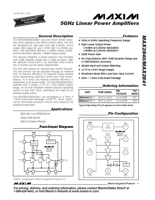
19-2494; Rev 2; 8/03 EVAALVUAAILTAIOBNLEKIT
5GHz Linear Power Amplifiers
MAX2840/MAX2841
General Description
The MAX2840/MAX2841 low-cost linear power amplifiers (PAs) operate in the 5GHz to 6GHz band. The PAs are designed for high gain and high linearity, which makes them ideal for use in IEEE 802.11a OFDM systems. The MAX2840 delivers +15dBm output power, and the MAX2841 delivers +18dBm output power.
NSD288板卡规格书

深圳市深北星科技有限公司安卓驱动板规格书(型号:NSD288)编号:NO.20180320001版本:Ver1.1编制:卢新泰审核:颜如城发布日期:2018-03-20目录目录 (2)版本更改记录 (3)1、产品简介 (4)2、产品外观及接口示意图 (4)3、产品特点说明 (5)4、产品基本功能列表 (6)5、产品PCB尺寸 (7)6、产品接口定义说明 (7)7、使用要求 (13)版本更改记录1、产品简介本产品主芯片采用瑞芯微RK3288 四核Cortex-A17和Mali-T764高GPU,主频最高可达1.8GHz,支持4Kx2K硬解H.265的芯片,搭载Android 5.1系统,跑分最高达43000多,超强性能。
支持LVDS/HDMIOUT/EDP/HDMI IN 等多种接口。
服务端采用B/S架构并用MYSQL + APACH + PHP实现的,支持主流的Window 和Linux系统平台,功能丰富,操作简单。
2、产品外观及接口示意图3、产品特点★支持完全无缝切换(两个视频切换时不需停顿处理,不出现黑屏)★支持双屏异显功能★支持播放对屏幕任意比例划分的任务节目,可断点下载任务节目★支持播放按时间段和定时>插播>循环>垫片不同优先级任务节目★支持发布系统设置终端信息、5段定时开关机、时间段音量、终端名称、网络IP,查看终端设备的软件版本信息★板卡支持6GB内部 ROM空间,可用于下载安装APK和播放任务节目,并支持TF卡扩展32GB存储空间(可选);★支持信发系统制作好的任务节目与单机两种模式播放,任务节目优先级高于单机节目,★支持电容、红外触摸屏,支持添加红外感应器★支持本地、OTA升级已及IPS发布系统远程,方便系统更新★屏幕支持90度、180度、270度旋转★板子支持以太网、内置WiFi模块(802.11b/g/n)、4G模块上网功能和蓝牙4.0模块功能★支持简体、繁体和英文切换,可根据客户需要添加不同国家语言★支持U盘自动拷贝功能,方便无网络时更新节目★支持主播放窗口视频、图片、文本和播放窗口图片、文本混播支持图片、文本滚屏显示★支持行业主流USB/串口设备,打印机、刷卡器、密码键盘、指纹仪、摄像头、身份证识别、二维码扫描仪等4、产品基本功能列表电源适配器12V电源/支持遥控器触摸屏支持IIC触摸屏、USB触摸屏系统看门狗支持尺寸124.5*89*16mm 5、PCB尺寸图PCB:6 层板尺寸:124.5mm*89mm, 板厚1.6mm螺丝孔规格:∮3.2mm x 46、主要接口定义说明背光接口定义CON15 (6PIN/2.0)脚序号定义描述1 12V 直流电源2 12V 直流电源3 BL_ON 开关控制(高电平有效)电源接口定义CON12(6PIN/2.54)双路LVDS输出接口定义CON9 (30PIN/2.0)EDP输出接口定义(20PIN/2.0)HDMI IN接口定义(24PIN/2.0)LED、遥控按键板接口定义CON14(8PIN/2.0)喇叭输出接口定义CON4(4PIN/2.0)声音输出接口定义CON10(4PIN/2.0)声音输入接口定义CON10(4PIN/2.0)UART2接口定义CON18 (4PIN/2.0)IIC接口定义CON13 (6PIN/2.0)UART1接口定义CON1(4PIN/2.0)USB接口CON8/CON21/CON22(4PIN/2.0)。
环希工业280说明书
SCD-280八单元同步调节器1.产品概要SCD280为江阴市环希工业控制设备有限公司成熟产品。
本产品经过多年的工业现场考验和设计、工艺的不断完善,功能实用,抗干扰能力强,稳定可靠。
本产品的主要特点如下:☆内含八路独立可编程模拟单元,一路内部主给定,八路外部反馈输入,内带±5V反馈电源。
☆内部主给定可采用上升、下降端子外接按钮进行调节。
2.产品外观及端子分配端子说明:开关量信号输入端子:2(启停);4(故障输入);13(下降);6(上升)开关量信号输出端子:运行信号:53(常闭);54(常开);55(公共端)报警信号:50(常闭);51(常开);52(公共端)模拟量主给定端子:9(信号);10(信号)反馈量端子:29(1#反馈)27(2#反馈)25(3#反馈)23(4#反馈)21(5#反馈)19(6#反馈)17(7#反馈)15(8#反馈)输出量端子:30(1#输出)32(2#输出)34(3#输出)36(4#输出)38(5#输出)40(6#输出)42(7#输出)44(8#输出)P6-1江阴市环希工业控制设备有限公司1.GS2.R/S3.+24V4.Err5.GS6.UP7.+10V8.GND9.G110.G211.GND 12.+10V 13.DOWN 14.GND 15.GF816.GND 17.GF718.GND 19.GF620.GND 21.GF522.GND 23.GF424.GND 25.GF326.GND 27.GF228.GND 29.GF1+24V地启停端子+24V电源≤80mA 外部故障输入+24V地上升端子+10V参考电压信号地外部主给定一外部主给定二信号地+10V参考电压下降端子信号地反馈输入8信号地反馈输入7信号地反馈输入6信号地反馈输入5信号地反馈输入4信号地反馈输入3信号地反馈输入2信号地反馈输入130.V131.GND 32.V233.GND 34.V335.GND 36.V437.GND 38.V539.GND 40.V641.GND 42.V743.GND 44.V845.GND 46.+5V 47.GND 48.-5V 49./50.TB251.TC252.TA253.TB154.TC155.TA156.GND 57.L 58.N单元1输出信号地单元2输出信号地单元3输出信号地单元4输出信号地单元5输出信号地单元6输出信号地单元7输出信号地单元8输出信号地反馈用+5V电源≤50mA 信号地反馈用-5V电源≤50mA 空脚报警信号常闭端报警信号常开端报警信号公共端运行信号常闭端运行信号常开端运行信号公共端开关电源接地端电源输入 220VAC 电源输入±20%50Hz参考电压端子:7,12(+10V)负载能力10mA46,48(±5V)负载能力200mA3(+24V)负载能力0.7A地端子:信号地:8,11,14,16,18,20,22,24,26,28,31,33,35,39,39,41,43,45,47。
TL288CP,TL288CPE4, 规格书,Datasheet 资料
1POST OFFICE BOX 655303 •DALLAS, TEXAS 75265DHigh Input Impedance . . . JFET-Input Stage1OUT 1IN −1IN+V CC −NC − No internal connectionIN V CC TL087, TL088D, JG, OR P PACKAGE(TOP VIEW)12348765V CC +2OUT 2IN −2IN+TL287, TL288JG OR P PACKAGE(TOP VIEW)IN V CC CC+TL088M U PACKAGE (TOP VIEW)1IN V CC CC +−TL288M U PACKAGE (TOP VIEW)description/ordering informationThese JFET-input operational amplifiers incorporate well-matched high-voltage JFET and bipolar transistors in a monolithic integrated circuit. They feature low input offset voltage, high slew rate, low input bias and offset currents, and low temperature coefficient of input offset voltage. Offset-voltage adjustment is provided for the TL087 and TL088.The C-suffix devices are characterized for operation from 0°C to 70°C, and the I-suffix devices are characterized for operation from −40°C to 85°C. The M-suffix devices are characterized for operation over the full military temperature range of −55°C to 125°C.ORDERING INFORMATIONT A TYPE V IO MAX AT 255C PACKAGE †ORDERABLE PART NUMBER TOP-SIDE MARKING 0°C to 70°CDual1 mVPDIP (P)Tube of 50TL288CPTL288CP†Package drawings, standard packing quantities, thermal data, symbolization, and PCB design guidelines are available at /sc/package.Copyright © 2004, Texas Instruments IncorporatedPRODUCTION DATA information is current as of publication date.Products conform to specifications per the terms of Texas Instruments standard warranty. Production processing does not necessarily include testing of all parameters.Please be aware that an important notice concerning availability, standard warranty, and use in critical applications of Texas Instruments semiconductor products and disclaimers thereto appears at the end of this data sheet.The TL087, TL088, and TL287 are obsolete and are no longer supplied.TL087, TL088, TL287, TL288JFET-INPUT OPERATIONAL AMPLIFIERSSLOS082B – MARCH 1979 REVISED – JULY 20042POST OFFICE BOX 655303 •DALLAS, TEXAS 75265symbol (each amplifier)+−OUTIN +IN −absolute maximum ratings over operating free-air temperature range (unless otherwise noted)TL088M TL288MTL087I TL088I TL287I TL288I TL087C TL088C TL287C TL288CUNITSupply voltage, VCC + (see Note 1)181818V Supply voltage, V CC − (see Note 1)−18−18−18V Differential input voltage (see Note 2)±30±30±30V Input voltage (see Notes 1 and 3)±15±15±15V Input current, I I (each Input )±1±1±1mA Output current, I O (each output)±80±80±80mA Total V CC + terminal current 160160160mA Total V CC − terminal current−160−160−160mADuration of output short circuit (see Note 4)UnlimitedUnlimited Unlimited Continuous total dissipation See Dissipation Rating TableMaximum junction temperature, T J150150°C Package thermal impedance, q JA (see Notes 5 and 6)P package 8585°C/W Lead temperature 1,6 mm (1/16 inch) from case for 60secondsJG or U package300300300°C Storage temperature range, T stg −65 to 150−65 to 150−65 to 150°C NOTES:1.All voltage values, except differential voltages, are with respect to the midpoint between V CC+ and V CC−.2.Differential voltages are at the noninverting input terminal with respect to the inverting input terminal.3.The magnitude of the input voltage must never exceed the magnitude of the supply voltage or 15 V, whichever is less.4.The output may be shorted to ground or to either supply. Temperature and/or supply voltages must be limited to ensure that the dissipation rating is not exceeded.5.Maximum power dissipation is a function of T J (max), q JA , and T A . The maximum allowable power dissipation at any allowable ambient temperature is PD = (T J (max) – T A )/q JA . Operating at the absolute maximum T J of 150°C can affect reliability.6.The package thermal impedance is calculated in accordance with JESD 51-7.7.The output may be shorted to ground or to either supply. Temperature and/or supply voltages must be limited to ensure that the dissipation rating is not exceeded.8.Maximum power dissipation is a function of T J (max), q JA , and T A . The maximum allowable power dissipation at any allowable ambient temperature is PD = (T J (max) – T A )/q JA . Operating at the absolute maximum T J of 150°C can affect reliability.9.The package thermal impedance is calculated in accordance with JESD 51-7.DISSIPATION RATING TABLEPACKAGET A ≤ 25°C POWER RATINGDERATING FACTOR ABOVE T A = 25°CT A = 70°C POWER RATINGT A = 85°C POWER RATINGT A = 125°C POWER RATINGJG 1050 mW 8.4 mW/°C 672 mW 546 mW 210 mW U675 mW5.4 mW/°C432 mW351 mW135 mWThe TL087, TL088, and TL287 are obsolete and are no longer supplied.TL087, TL088, TL287, TL288JFET-INPUT OPERATIONAL AMPLIFIERSSLOS082B – MARCH 1979 REVISED – JULY 20043POST OFFICE BOX 655303 •DALLAS, TEXAS 75265recommended operating conditionsC-SUFFIX I-SUFFIX M-SUFFIX MINMAX MIN MAX MIN MAX UNIT V CC Supply voltage±5±5±5±5±5±15V Common mode input voltage V CC ± = ±5 V −14−14−14V IC Common-mode input voltage V CC ± = ±15 V −1111−1111−1111V Input voltage V CC ± = ±5 V −14−14−14V I Input voltageV CC ± = ±15 V−1111−1111−1111V T AOperating free-air temperature70−4085−55125°Coperating characteristics V CC = ±15 V, T A = 25°CTL088M, TL288M TL087I, TL087C TL088I, TL088C PARAMETERTEST CONDITIONSMINTYP MAXMIN TYP MAXUNITSR Slew rate at unity gain V I = 10 V,C L = 100 pF,R L = 2 k Ω,A VD = 118818V/μs t r Rise time V I = 20 mV,R L = 2 k Ω,5555ns Overshoot factorC L = 100 pF,A VD = 12525%V nEquivalent input noise voltageR S = 100 Ω,f = 1 kHz1919nV/√HzTL087, TL088, TL287, TL288JFET-INPUT OPERATIONAL AMPLIFIERSSLOS082B – MARCH 1979 – REVISED – JULY 20045POST OFFICE BOX 655303 •DALLAS, TEXAS 75265PARAMETER MEASUREMENT INFORMATIONV I+−V CC +V CC −V OC L(see Note A)Overshoot10%90%t r − Rise TimeR LNOTE A: C L includes fixture capacitance.Figure 1. Slew Rate, Rise/Fall Time,Figure 2. Rise Time and Overshootand Overshoot Test Circuit WaveformV CC −V CC +V OC LV OV CC −V CC +R SR S10 k ΩR LV I10 k Ω100NOTE A: C L includes fixture capacitance.+−+−(see Note A)Figure 3. Noise Voltage Test CircuitFigure 4. Unity-Gain Brandwidth andPhase Margin Test CircuitpAV CC +V CC −Ground ShieldpAFigure 5. Input Bias and OffsetCurrent Test Circuit+−TL087, TL088, TL287, TL288JFET-INPUT OPERATIONAL AMPLIFIERSSLOS082B – MARCH 1979 – REVISED – JULY 20046POST OFFICE BOX 655303 •DALLAS, TEXAS 75265typical valuesTypical values as presented in this data sheet represent the median (50% point) of device parametric performance.input bias and offset currentAt the picoamp bias current level typical of these JFET operational amplifiers, accurate measurement of the bias current becomes difficult. Not only does this measurement require a picoammeter, but test socket leakages can easily exceed the actual device bias currents. T o accurately measure these small currents, Texas Instruments uses a two-step process. The socket leakage is measured using picoammeters with bias voltages applied, but with no device in the socket. The device then is inserted in the socket and a second test that measures both the socket leakage and the device input bias current is performed. The two measurements then are subtracted algebraically to determine the bias current of the device.TL087, TL088, TL287, TL288JFET-INPUT OPERATIONAL AMPLIFIERSSLOS082B – MARCH 1979 – REVISED – JULY 20047POST OFFICE BOX 655303 •DALLAS, TEXAS 75265TYPICAL CHARACTERISTICStable of graphsFIGUREαVIOTemperature coefficient of input offset voltage Distribution 6, 7I IO Input offset current vs Temperature 8I IB Input bias currentvs V ICvs Temperature 98V I Common-mode input voltage range limits vs V CCvs Temperature 1011V ID Differential input voltagevs Output voltage 12V OMMaximum peak output voltage swingvs V CCvs Output current vs Frequency vs Temperature 131714, 15, 1618A VD Differential voltage amplification vs R Lvs Frequency vs Temperature 192021z o Output impedancevs Frequency 24CMRR Common-mode rejection ratio vs Frequency vs Temperature 2223k SVR Supply-voltage rejection ratio vs Temperature 25I OS Short-circuit output currentvs V CC vs Timevs Temperature 262728I CC Supply current vs V CCvs Temperature 2930SRSlew rate vs R Lvs Temperature 3132Overshoot factorvs C L33V n Equivalent input noise voltage vs Frequency 34THD Total harmonic distortion vs Frequency 35B 1Unity-gain bandwidthvs V CCvs Temperature 3637φmPhase margin vs V CC vs C Lvs Temperature 383940Phase shift vs Frequency 20Pulse responseSmall-signal Large-signal4142TL087, TL088, TL287, TL288JFET-INPUT OPERATIONAL AMPLIFIERSSLOS082B – MARCH 1979 – REVISED – JULY 20048POST OFFICE BOX 655303 •DALLAS, TEXAS 75265TYPICAL CHARACTERISTICS †−2502520−20−15−10−505101520481216P e r c e n t a g e o f A m p l i f i e r s − %−300αVIO − Temperature Coefficient − μV/°C−20−10010205αVIO − Temperature Coefficient − μV/°CDISTRIBUTION OF TL088INPUT OFFSET VOLTAGE TEMPERATURE COEFFICIENTDISTRIBUTION OF TL288INPUT OFFSET VOLTAGE TEMPERATURE COEFFICIENTP e r c e n t a g e o f U n i t s − %Figure 6Figure 7T A − Free-Air Temperature − °C I B a n d I I O− B i a s a n d O f f s e t C u r r e n t s − n A0.001250.010.1110100456585105125−15−10I I B − I n p u t B i a s C u r r e n t − n AV IC − Common-Mode Input Voltage − V−5510−10−5051015T A = 25°CINPUT BIAS CURRENT AND INPUT OFFSET CURRENTvsFREE-AIR TEMPERATUREINPUT BIAS CURRENTvsCOMMON-MODE INPUT VOLTAGEV CC ± = ±15 V I B I I O I B Figure 8Figure 9†Data at high and low temperatures are applicable within the rated operating free-air temperature ranges of the various devices.TL087, TL088, TL287, TL288JFET-INPUT OPERATIONAL AMPLIFIERSSLOS082B – MARCH 1979 – REVISED – JULY 20049POST OFFICE BOX 655303 •DALLAS, TEXAS 75265TYPICAL CHARACTERISTICS †−16V I C − C o m m o n -M o d e I n p u t V o l t q g e − V|V CC ±|− Supply Voltage − V−75−20T A − Free-Air Temperature − °C−8−40481216246810121416Negative LimitPositive Limit−15−10−505101520−50−250255075100125T A = 25°CCOMMON-MODEINPUT VOLTAGE RANGE LIMITSvsSUPPLY VOLTAGECOMMON-MODEINPUT VOLTAGE RANGE LIMITSvsFREE-AIR TEMPERATUREV I C −12V I C − C o m m o n -M o d e I n p u t V o l t q g e − VV I C Figure 10Figure 11−400−15O − O ut p u t V o l t a g e − VV ID − Differential Input Voltage − μV−10−551015−2000200400V CC ± = ±15 VT A = 25°CR L = 600 ΩR L = 1 k ΩR L = 2 k ΩR L = 10 k Ω0−16M a x i m u m P e a k O u t p u t V o l t a g e − V |V CC ±| − Supply Voltage − V−8−40481216246810121416T A = 25°CV OM +R L = 10 k ΩR L = 2 k ΩV OM −R L = 2 k ΩR L = 10 k ΩOUTPUT VOLTAGEvsDIFFERENTIAL INPUT VOLTAGEMAXIMUM PEAK OUTPUT VOLTAGEvsSUPPLY VOLTAGEV O Figure 12Figure 13†Data at high and low temperatures are applicable within the rated operating free-air temperature ranges of the various devices.TL087, TL088, TL287, TL288JFET-INPUT OPERATIONAL AMPLIFIERSSLOS082B – MARCH 1979 – REVISED – JULY 200410POST OFFICE BOX 655303 •DALLAS, TEXAS 75265TYPICAL CHARACTERISTICS †010 kf − Frequency − Hz010 kf − Frequency − Hz51015202530100 k 1 M 10 M51015202530100 k 1 M 10 MV CC ± = ±15 VV CC ± = ±5 VT A = 25°CR L = 2 k ΩMAXIMUM PEAK-TO-PEAK OUTPUT VOLTAGEvsFREQUENCYMAXIMUM PEAK-TO-PEAK OUTPUT VOLTAGEvsFREQUENCYV O P P − M a x i m u m P e a k -t o -P e a k O u t p u t V o l t a g e − V V O (PP )V O P P − M a x i m u m P e a k -t o -P e a k O u t p u t V o l t a g e − V V O (PP )Figure 14Figure 15MAXIMUM PEAK OUTPUT VOLTAGEvsOUTPUT CURRENT20253015105010 k100 k f − Frequency − Hz1 M 10 M00M a x i m u m P e a k O u t p u t V o l t a g e − V |I O | − Output Current − mA5016102030402468101214MAXIMUM PEAK-TO-PEAK OUTPUT VOLTAGEvsFREQUENCYV O P P − M a x i m u m P e a k -t o -P e a k O u t p u t V o l t a g e − V V O (PP )515253545Figure 16Figure 17†Data at high and low temperatures are applicable within the rated operating free-air temperature ranges of the various devices.TL087, TL088, TL287, TL288JFET-INPUT OPERATIONAL AMPLIFIERSSLOS082B – MARCH 1979 – REVISED – JULY 200411POST OFFICE BOX 655303 •DALLAS, TEXAS 75265TYPICAL CHARACTERISTICS †250A V D − D if f e r e n t i a l V o l t ag e A m p l i f i c a t i o n − V /m V0.40R L − Load Resistance − k Ω50100150200141040V O = ±1 VT A = 25°CV CC ± = ±15 VV CC ± = ±5 V−75−16M a x i m u m P e a k O u t p u t V o l t a g e − VT A − Free-Air Temperature − °C12516−50−25255075100−12−8−404812MAXIMUM PEAK OUTPUT VOLTAGEvsFREE-AIR TEMPERATURELARGE-SIGNAL VOLTAGE AMPLIFICATIONvsLOAD RESISTANCE100A V D Figure 18Figure 1910f − Frequency − Hz10 M1061001 k 10 k 100 k 1 M0.11101104105−75101251000−50−25025507510040100400102103T A − Free-Air Temperature − °C0°30°60°90°120°150°180°P h a s e S h i f tLARGE-SIGNAL DIFFERENTIAL VOLTAGE AMPLIFICATION AND PHASE SHIFTvsFREQUENCYLARGE-SIGNAL VOLTAGE AMPLIFICATIONvsFREE-AIR TEMPERATUREA V D − D i f f e r e n t i a l V o l t a g e A m p l i f i c a t i o n − V /m VA V D A V D − D i f f e r e n t i a l V o l t a g e A m p l i f i c a t i o n A V DFigure 20Figure 21†Data at high and low temperatures are applicable within the rated operating free-air temperature ranges of the various devices.TL087, TL088, TL287, TL288JFET-INPUT OPERATIONAL AMPLIFIERSSLOS082B – MARCH 1979 – REVISED – JULY 200412POST OFFICE BOX 655303 •DALLAS, TEXAS 75265TYPICAL CHARACTERISTICS †908070605040302010100C M R R − C o m m o n -M o d e R e j e c t i o n R a t i o − d B0 1 M100 k 10 k 1 k 10010 Mf − Frequency − Hz10V CC ± = ±15 V T A = 25°C−7570T A − Free-Air Temperature − °C1251007580859095−50−250255075100COMMON-MODE REJECTION RATIOvsFREQUENCYCOMMON-MODE REJECTION RATIOvsFREE-AIR TEMPERATUREC M R R − C o m m o n -M o d e R e j e c t i o n R a t i o − d BFigure 22Figure 231 k0.1z 0 − O u t p u t I n p p e d a n c e − 1 M10010 k100 k110f − Frequency − HzA VD = 100A VD = 10A VD = 1V CC ± = ±15 VT A = 25°Cr o (open loop) ≈ 250 Ω−7590k S V R − S u p p l y -V o l t a g e R e j e c t i o n R a t i o − d B T A − Free-Air Temperature − °C125110−50−2502550751009498102106OUTPUT IMPEDANCEvsFREQUENCYSUPPLY-VOLTAGE REJECTION RATIOvsFREE-AIR TEMPERATURES V Rk Ωo Figure 24Figure 25†Data at high and low temperatures are applicable within the rated operating free-air temperature ranges of the various devices.TL087, TL088, TL287, TL288JFET-INPUT OPERATIONAL AMPLIFIERSSLOS082B – MARCH 1979 – REVISED – JULY 200413POST OFFICE BOX 655303 •DALLAS, TEXAS 75265TYPICAL CHARACTERISTICS †−60|V CC ±| − Supply Voltage − V16602468101214−40−2002040Time − Seconds4020−20−4060−606050403020100V O = 0T A = 25°CV ID = 1 VT A = 25°CV ID = − 1 VV CC ± = ±15 V V ID = 1 VV ID = −1 VO S − S h o r t -C i r c u i t O u t p u t C u r r e n t − m ASHORT-CIRCUIT OUTPUT CURRENTvsSUPPLY VOLTAGESHORT-CIRCUIT OUTPUT CURRENTvs TIMEO S I O S − S h o r t -C i r c u i t O u t p u t C u r r e n t − m AO S I Figure 26Figure 27T A − Free-Air Temperature − °C4020−20−4060−601007550250−25−50125−75V CC ± = ±15 VV CC ± = ±5 VV CC ± = ±5 VV CC ± = ±15 VV ID = 1 VV ID = 1 VV ID = −1 VV ID = −1 V V O = 0SHORT-CIRCUIT OUTPUT CURRENTvsFREE-AIR TEMPERATUREO S − S h o r t -C i r c u i t O u t p u t C u r r e n t − m AO S I Figure 28†Data at high and low temperatures are applicable within the rated operating free-air temperature ranges of the various devices.TL087, TL088, TL287, TL288JFET-INPUT OPERATIONAL AMPLIFIERSSLOS082B – MARCH 1979 – REVISED – JULY 200414POST OFFICE BOX 655303 •DALLAS, TEXAS 75265TYPICAL CHARACTERISTICS †0C C − S u p p l y C u r r e n t − m A|V CC ±| − Supply Voltage − V16324681012140.511.522.5−7501253−50−252550751000.511.522.5T A − Free-Air Temperature − °CT A = 25°CT A = −55°C TA = 125°CV O = 0No LoadV CC ± = ±5 VV CC ± = ±15 VV O = 0No LoadSUPPLY CURRENTvsFREE-AIR TEMPERATURESUPPLY CURRENTvsSUPPLY VOLTAGEC C I I C C − S u p p l y C u r r e n t − m AC C Figure 29Figure 302500.4S R − S l e w R a t e − V /s R L − Load Resistance − k Ω510152030141040100−750T A − Free-Air Temperature − °C12530−50−250255075100510152025V CC ± = ±15 V R L = 2 k ΩC L = 100 pF See Figure 1SLEW RATEvsLOAD RESISTANCESLEW RATEvsFREE-AIR TEMPERATURESR +SR −sμS R − S l e w R a t e − V /s sμFigure 31Figure 32†Data at high and low temperatures are applicable within the rated operating free-air temperature ranges of the various devices.TL087, TL088, TL287, TL288JFET-INPUT OPERATIONAL AMPLIFIERSSLOS082B – MARCH 1979 – REVISED – JULY 200415POST OFFICE BOX 655303 •DALLAS, TEXAS 75265TYPICAL CHARACTERISTICS †O v e r s h o o t F a c t o r − %C L − Load Capacitance − pF300505010015020025010203040 f − Frequency − Hz10V n − E q u i v a le n t I n p u t N o i s e V o l t a g e 102030405070100100 1 k 10 k 100 kSee Figure 1T A = 25°C R L = 2 k ΩV I(PP) = ±10 mVV CC ± = ±5 VV CC ± = ±15 VOVERSHOOT FACTORvsLOAD CAPACITANCEEQUIVALENT INPUT NOISE VOLTAGEvsFREQUENCYnFigure 33Figure 342.7B 1 − U n i t y -G a i n B a n d w i d t h − M H z|V CC ±| − Supply Voltage − V163.224681012142.82.933.10.001100f − Frequency − HzT H D − T o t a l H a r m o n i c D i s t o r t i o n − %0.010.111 k 10 k 100 kV I = 10 mV R L = 2 k ΩC L = 25 pF T A = 25°C See Figure 4TOTAL HARMONIC DISTORTIONvsFREQUENCYUNITY-GAIN BANDWIDTHvsSUPPLY VOLTAGE1Figure 35Figure 36†Data at high and low temperatures are applicable within the rated operating free-air temperature ranges of the various devices.TL087, TL088, TL287, TL288JFET-INPUT OPERATIONAL AMPLIFIERSSLOS082B – MARCH 1979 – REVISED – JULY 200416POST OFFICE BOX 655303 •DALLAS, TEXAS 75265TYPICAL CHARACTERISTICS †−750T A − Free-Air Temperature − °C1254−50−2525507510012355°m − P h a s e M a r g i n1665°246810121457°59°61°63°|V CC ±| − Supply Voltage − VSee Figure 4V I = 10 mV R L = 2 k ΩC L = 25 pF V CC ± = ±15 VV CC ± = ±5 VSee Figure 4T A = 25°C C L = 25 pF R L = 2 k ΩV I = 10 mVUNITY-GAIN BANDWIDTHvsFREE-AIR TEMPERATUREPHASE MARGINvsSUPPLY VOLTAGEB 1 − U n i t y -G a i n B a n d w i d t h − M H z1m φFigure 37Figure 38V I = 10 mV40°C L − Load Capacitance − pF10070°10203040506070809045°50°55°60°65°−7555°T A − Free-Air Temperature − °C12565°−50−2525507510057°59°61°63°V I = 10 mV R L = 2 k ΩT A = 25°C See Figure 4V CC ± = ±15 VC L = 25 pF R L = 2 k ΩSee Figure 4V CC ± = ±15 VV CC ± = ±5 VV CC ± = ±5 VPHASE MARGINvsLOAD CAPACITANCEPHASE MARGINvsFREE-AIR TEMPERATUREm − P h a s e M a r g i n mφm − P h a s e M a r g i n mφFigure 39Figure 40†Data at high and low temperatures are applicable within the rated operating free-air temperature ranges of the various devices.TL087, TL088, TL287, TL288JFET-INPUT OPERATIONAL AMPLIFIERSSLOS082B – MARCH 1979 – REVISED – JULY 200417POST OFFICE BOX 655303 •DALLAS, TEXAS 75265TYPICAL CHARACTERISTICS−8t − Time − μs68012345−6−4−20246−16V O − O u t p u t V o l t a g e − m Vt − Time − μs1.21600.20.40.60.81.0−12−8−404812V CC ± = ±15 V R L = 2 k ΩC L = 100 pF T A = 25°C See Figure 1V CC ± = ±15 VR L = 2 k ΩC L = 100 pF T A = 25°C See Figure 1VOLTAGE-FOLLOWERSMALL-SIGNAL PULSE RESPONSEVOLTAGE-FOLLOWERLARGE-SIGNAL PULSE RESPONSEV O V O − O u t p u t V o l t a g e − m VV O Figure 41Figure 42TL087, TL088, TL287, TL288JFET-INPUT OPERATIONAL AMPLIFIERSSLOS082B – MARCH 1979 – REVISED – JULY 200418POST OFFICE BOX 655303 •DALLAS, TEXAS 75265TYPICAL APPLICATION DATAoutput characteristicsAll operating characteristics are specified with 100-pF load capacitance. These amplifiers will drive higher capacitive loads; however, as the load capacitance increases, the resulting response pole occurs at lower frequencies, causing ringing, peaking, or even oscillation. The value of the load capacitance at which oscillation occurs varies with production lots. If an application appears to be sensitive to oscillation due to load capacitance,adding a small resistance in series with the load should alleviate the problem. Capacitive loads of 1000 pF , andlarger, may be driven if enough resistance is added in series with the output (see Figure 43).(a) C L = 100 pF, R = 0(b) C L = 300 pF, R = 0(c) C L = 350 pF, R = 0(d) C L = 1000 pF, R = 0(e) C L = 1000 pF, R = 50 Ω(f) C L = 1000 pF, R = 2 k ΩFigure 43. Effect of Capacitive Loads+−5 V −5 V15 V−15 V2 k ΩV ORNOTE A: C L includes fixture capacitanceC L(see Note A)Figure 44. Test Circuit for Output CharacteristicsTL087, TL088, TL287, TL288JFET-INPUT OPERATIONAL AMPLIFIERSSLOS082B – MARCH 1979 – REVISED – JULY 200419POST OFFICE BOX 655303 •DALLAS, TEXAS 75265TYPICAL APPLICATION DATAinput characteristicsThese amplifiers are specified with a minimum and a maximum input voltage that, if exceeded at either input,could cause the device to malfunction.Because of the extremely high input impedance and resulting low bias current requirements, these amplifiers are well suited for low-level signal processing; however, leakage currents on printed circuit boards and sockets easily can exceed bias current requirements and cause degradation in system performance. It is good practice to include guard rings around inputs (see Figure 45). These guards should be driven from a low-impedance source at the same voltage level as the common-mode input.+−+−+−V OV OV OV IV I(a) NONINVERTING AMPLIFIER(b) INVERTING AMPLIFIER(c) UNITY−GAIN AMPLIFIERV IFigure 45. Use of Guard Ringsnoise performanceThe noise specifications in operational amplifier circuits are greatly dependent on the current in the first-stage diflferential amplifier. The low input bias current requirements of these amplifiers result in a very low current noise. This feature makes the devices especially favorable over bipolar devices when using values of circuit impedance greater than 50 k Ω.PACKAGING INFORMATIONOrderable DeviceStatus (1)Package Type Package DrawingPins Package Qty Eco Plan (2)Lead/Ball Finish MSL Peak Temp (3)TL288CP ACTIVE PDIP P 850Pb-Free (RoHS)CU NIPDAU N /A for Pkg Type TL288CPE4ACTIVEPDIPP850Pb-Free (RoHS)CU NIPDAUN /A for Pkg Type(1)The marketing status values are defined as follows:ACTIVE:Product device recommended for new designs.LIFEBUY:TI has announced that the device will be discontinued,and a lifetime-buy period is in effect.NRND:Not recommended for new designs.Device is in production to support existing customers,but TI does not recommend using this part in a new design.PREVIEW:Device has been announced but is not in production.Samples may or may not be available.OBSOLETE:TI has discontinued the production of the device.(2)Eco Plan -The planned eco-friendly classification:Pb-Free (RoHS),Pb-Free (RoHS Exempt),or Green (RoHS &no Sb/Br)-please check /productcontent for the latest availability information and additional product content details.TBD:The Pb-Free/Green conversion plan has not been defined.Pb-Free (RoHS):TI's terms "Lead-Free"or "Pb-Free"mean semiconductor products that are compatible with the current RoHS requirements for all 6substances,including the requirement that lead not exceed 0.1%by weight in homogeneous materials.Where designed to be soldered at high temperatures,TI Pb-Free products are suitable for use in specified lead-free processes.Pb-Free (RoHS Exempt):This component has a RoHS exemption for either 1)lead-based flip-chip solder bumps used between the die and package,or 2)lead-based die adhesive used between the die and leadframe.The component is otherwise considered Pb-Free (RoHS compatible)as defined above.Green (RoHS &no Sb/Br):TI defines "Green"to mean Pb-Free (RoHS compatible),and free of Bromine (Br)and Antimony (Sb)based flame retardants (Br or Sb do not exceed 0.1%by weight in homogeneous material)(3)MSL,Peak Temp.--The Moisture Sensitivity Level rating according to the JEDEC industry standard classifications,and peak solder temperature.Important Information and Disclaimer:The information provided on this page represents TI's knowledge and belief as of the date that it is provided.TI bases its knowledge and belief on information provided by third parties,and makes no representation or warranty as to the accuracy of such information.Efforts are underway to better integrate information from third parties.TI has taken and continues to take reasonable steps to provide representative and accurate information butmay not have conducted destructive testing or chemical analysis on incoming materials and chemicals.TI and TI suppliers consider certain information to be proprietary,and thus CAS numbers and other limited information may not be available for release.In no event shall TI's liability arising out of such information exceed the total purchase price of the TI part(s)at issue in this document sold by TI to Customer on an annual basis.PACKAGE OPTION ADDENDUM9-Feb-2007Addendum-Page 1。
288P中文资料
R1.125 [28.575]S±0.062 [1.575] Document Number: 42023For technical questions, contact spresale@Document Number: 42023For technical questions, contact spresale@Legal Disclaimer NoticeVishay Document Number: NoticeSpecifications of the products displayed herein are subject to change without notice. Vishay Intertechnology, Inc., or anyone on its behalf, assumes no responsibility or liability for any errors or inaccuracies.Information contained herein is intended to provide a product description only. No license, express or implied, by estoppel or otherwise, to any intellectual property rights is granted by this document. Except as provided in Vishay's terms and conditions of sale for such products, Vishay assumes no liability whatsoever, and disclaims any express or implied warranty, relating to sale and/or use of Vishay products including liability or warranties relating to fitness for a particular purpose, merchantability, or infringement of any patent, copyright, or other intellectual property right. The products shown herein are not designed for use in medical, life-saving, or life-sustaining applications. Customers using or selling these products for use in such applications do so at their own risk and agree to fully indemnify Vishay for any damages resulting from such improper use or sale.。
原子吸收光谱仪对比-科邦实验室-2020.6.23
光电倍增管
火焰气路 控制
内置石墨炉观测系统,为 可选件,成像模糊。
火焰采用氘灯扣背景 280Z 为横向塞曼扣背景,有偏振 镜,光能量损失严重。
火焰采用氘灯背景,石墨炉 为横向塞曼扣背景,有偏振 镜,光能量损失严重。含量 低时塞曼无法检测,只能以 氘灯扣背景进行测量。
全国原子光谱工程师约 30 人 应用工程师约 8 人
全国原子光谱工程师约 30 人 应用工程师约 5 人
铌合金/位置可调/角度可调
全钛/位置可调/角度可调
只有纵向加热
只有纵向加热
横向加热
只有空心阴极灯,测量 As、Se、Hg 时存在困难
≥0.2 Abs
合金/位置不可调/角度不 可调
只有纵向加热
只要是空心阴极 灯就不能用于测 定 As,Se 等元 素或得到较好的 结果。
塞曼扣背景的火 焰法灵敏度最 低。
燃烧头位置和角 度的调整可以扩 展检测线性范 围,得到更好的 检测效果。
横向加热无稳定 梯度,保证石墨 管内的温度均匀 一致。
最大升温 速率
2000℃/s
最高原子 化温度
2600℃
石墨炉自 动进样器 88/148 位
位数
石墨炉电 源
内置直流石墨炉电源
石墨炉观 测
内置彩色高清晰数码摄像机 和摄像光纤,使用方便且无 故障,丝毫不影响主机性 能。
随主机内置在仪器中。
5ppm 铜 ≥1.0 Abs
燃烧头 全钛/位置可调/角度可调
瀚斯宝丽使用说明
第 3 章:输入文本 . . . . . . . . . . . . . . . . . . . . . . . . . . . . . . . . . . . . 18
文本输入方法 . . . . . . . . . . . . . . . . . . . . . . . . . . . . . . . . . . . . . . . 18 使用 (QWERTY) 键盘输入文本 . . . . . . . . . . . . . . . . . . . . . . . . . . 18 使用符号 / 数字模式 . . . . . . . . . . . . . . . . . . . . . . . . . . . . . . . . . . 18 . . . . . . . . . . . . . . . . . . . . . . . . . . . . . . . . . . . . 27
硬件连接 . . . . . . . . . . . . . . . . . . . . . . . . . . . . . . . . . . . . . . . . . . . 电脑连接 . . . . . . . . . . . . . . . . . . . . . . . . . . . . . . . . . . . . . . . . 存储卡 . . . . . . . . . . . . . . . . . . . . . . . . . . . . . . . . . . . . . . . . . . 附件连接 . . . . . . . . . . . . . . . . . . . . . . . . . . . . . . . . . . . . . . . . 软件连接 . . . . . . . . . . . . . . . . . . . . . . . . . . . . . . . . . . . . . . . . . . . 浏览器 . . . . . . . . . . . . . . . . . . . . . . . . . . . . . . . . . . . . . . . . . . Wi-Fi . . . . . . . . . . . . . . . . . . . . . . . . . . . . . . . . . . . . . . . . . . . 蓝牙 . . . . . . . . . . . . . . . . . . . . . . . . . . . . . . . . . . . . . . . . . . . . 虚拟专用网 (VPN) . . . . . . . . . . . . . . . . . . . . . . . . . . . . . . . . . 27 27 27 28 29 29 30 30 30
- 1、下载文档前请自行甄别文档内容的完整性,平台不提供额外的编辑、内容补充、找答案等附加服务。
- 2、"仅部分预览"的文档,不可在线预览部分如存在完整性等问题,可反馈申请退款(可完整预览的文档不适用该条件!)。
- 3、如文档侵犯您的权益,请联系客服反馈,我们会尽快为您处理(人工客服工作时间:9:00-18:30)。
AXP288SCH Design Guide
1BUCK
1.1The inductor value should be1.0uH,the saturation current should be1.5times or more than the maximum current,and dc resistance should be lesser than100mΩ.
1.2The input capacitors value should be more than10uF.
1.3The output capacitors value should be more than10uF,and larger capacitors can be used to reduce output ripple.
1.4When BUCK4SET connecting to GND,output voltage of BUCK4is1.5V default;When BUCK4SET floating,output voltage of BUCK4is1.24V default;When BUCK4SET connecting to VINT,output voltage of BUCK4is1.36V default.
2Charger
2.1The inductor value should be1.0uH,the saturation current should be1.5times or more than the maximum current,and dc resistance should be lesser than100mΩ.
2.2The input capacitor value should be more than10uF.
2.3The output capacitor value should be more than10uF.
2.4The value of sampling resistance for battery current should be10mΩand1%accuracy,and the package should be more than0805.
2.5Two10uF capacitors should be connected to the pads of sampling resistance respectively,and a1uF capacitor should be connected in parallel with the sampling resistance.
2.6TS pin should be connected to NTC thermistor if needing battery temperature detection;if not, TS pin should be connected to a10K resistance,or left it floating and disable the temperature detection function through software.
2.7CHGLED pin can be used for the LED of charger state indication;if no need this function,left it floating.Note that CHGLED is an open drain structure and needs to pull up to other power.
3LDO
3.1The output capacitor of VCC_RTC should be10uF.
3.2ALDOIN should connect to PS,input capacitor value should be more than
4.7uF,and value of output capacitors of ALDO1/2/3should be4.7~10uF.
3.3DLDOIN can connect to PS or VBAT-EXT,input capacitor value should be more than
4.7uF, and value of the output capacitors of DLDO1/2/3/4should be4.7~10uF.
3.4ELDOIN/FLDOIN can connect to PS,VBAT-EXT or BUCK output,input capacitor value should be more than
4.7uF,and value of the output capacitors of ELDO1/2/3,FLDO1/2/3should be4.7~10uF.
4IPS
4.1The value of input capacitor of VBUS1/VBUS2should be more than4.7uF,and the withstand voltage should be more than16V.
4.2The value of output capacitor of PS should be more than10uF,and the withstand voltage should be more than10V.
4.3The PMOS connecting BAT-EXT to PS should satisfy that Vth<1.5V and resistance is less than30mΩwhen Vgs=4.5V.
4.43G module and the load needing larger current can be powered by VBAT-EXT.
4.5For the application with no battery,IPS and Charger should be modified as below:
(1)delete the inductor,sampling resistance and corresponding filter capacitors,and input capacitor of charger.
(2)delete the PMOS of IPS.
(3)add a diode connecting PS to BATSENSE.
(4)connect BATSENSE to LOADSENSE.
(5)VIN_CHG should connect to PS.
As the figure shown below:
5Others
5.1PWRON pin can be used to power on and power off to add a key in this pin.
5.2CORWPWROK pin can be used to reset to add a key in this pin.
5.3RSMRST_B should be pulled up,and it is recommended to pull up to ALDO3.
5.4IRQ should be pulled up,and it is recommended to pull up to VCC_RTC.。