LT1937中文资料
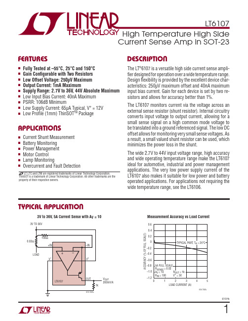
LT6107中文资料
TEMPERATURE RANGE –55°C to 150°C
TEMPERATURE RANGE –55°C to 150°C
ELECTRICAL CHARACTERISTICS The ● denotes the specifications which apply over the full specified
0
VSENSE = 500mV, RIN = 500Ω, ROUT = 10k, V+ = 36V ● –0.45 –0.14
0.1
VOUT(HIGH)
Output Swing High (Referred to V+)
VSENSE = 120mV
1.2
●
1.4
μV μV μV/°C
nA nA nA
VSENSE = 5mV V+ = 12V, 36V
●
1
40
●
130
IOS
Input Offset Current
V+ = 12V, 36V
1
IOUT PSRR
Maximum Output Current Power Supply Rejection Ratio
(Note 3) V+ = 2.7V to 36V, VSENSE = 5mV
SYMBOL
BW tr IS
PARAMETER
CONDITIONS
MIN
Байду номын сангаас
Minimum Output Voltage (Note 5)
VSENSE = 0mV, RIN = 100Ω, ROUT = 10k ●
VSENSE = 0mV, RIN = 500Ω, ROUT = 10k, V+ = 12V, 36V ●
2SK1937-01中文资料

2SK1937-01
FAP-IIA Series
> Features
- High Speed Switching - Low On-Resistance - No Secondary Breakdown - Low Driving Power - High Voltage - VGS = ± 30V Guarantee - Avalanche Proof
↑
7
↑
8
↑↑
9
VGS [V] IF [A]
VDS [V]
C [nF]
→ VDS [V]
Allowable Power Dissipation vs. TC
↑
பைடு நூலகம்10
↑
→ Qg [nC]
Safe operation area
↑
12
Zth(ch-c) [K/W]
→ VSD [V]
Transient Thermal impedance
tf
RGS=10 Ω
Avalanche Capability
I AV
L = 100µH Tch=25°C
Continous Reverse Drain Current
I DR
Pulsed Reverse Drain Current
I DRM
Diode Forward On-Voltage
V SD
IF=2xIDR VGS=0V Tch=25°C
> Applications
- Switching Regulators - UPS - DC-DC converters - General Purpose Power Amplifier
2SA1937中文资料

TOSHIBA
2-7B1A
Weight: 0.36 g (typ.)
absolute maximum ratings.
Please design the appropriate reliability upon reviewing the Toshiba Semiconductor Reliability Handbook
IB1 2 kΩ
tstg
IB2 IB2
―
2.3
―
μs
VCC = −200 V
Fall time
tf
IB1 = −10 mA, IB2 = 20 mA,
DUTY CYCLE ≤ 1%
―
0.2
―
Marking
A1937
Part No. (or abbreviation code)
Lot No.
A line indicates lead (Pb)-free package or lead (Pb)-free finish.
2
2006-11-09
Collector current IC (mA)
−500 −400 −300
IC – VCE
−100 −80 −60 −40
−20 −10 −5 −2
−1
−0.5 −200
−100
0 0
IB = −0.2 mA
Common emitter Tc = 25°C
−4
−8
−12
−16
Collector-emitter saturation voltage VCE (sat) (V)
VCE (sat) – IC
−30 Common emitter
LT1943_1资料

5ms/DIV123456GND (Pins 1, 20, Exposed Pad Pin 29): Ground. Tie both GND pins and the exposed pad directly to a local ground plane. The ground metal to the exposed pad should be as wide as possible for better heat dissipation. Multiple vias (to ground plane under the ground backplane) placed close to the exposed pad can further aid in reducing thermal resistance.VC1 (Pin 2): Switching Regulator 1 Error Amplifier Com-pensation. Connect a resistor/capacitor network in series with this pin.VC2 (Pin 3): Error Amplifier Compensation for Switcher2. Connect a resistor/capacitor network in series with this pin.FB1 (Pin 4): Switching Regulator 1 Feedback. Tie the resistor divider tap to this pin and set V LOGIC according to V LOGIC = 1.25 • (1 + R2/R1). Reference designators refer to Figure 1.FB2 (Pin 5): Feedback for Switch 2. Tie the resistor divider tap to this pin and set AV DD according to AV DD = 1.25 •(1 + R6/R5).FB3 (Pin 6): Switching Regulator 3 Feedback. Tie the resistor divider tap to this pin and set V ON according to V ON = 1.25 • (1 + R9/R8) – 150mV.NFB4 (Pin 7): Switching Regulator 4 Negative Feedback. Switcher 4 can be used to generate a positive or negative output. When regulating a negative output, tie the resistor divider tap to this pin. Negative output voltage can be set by the equation V OFF = –1.245 • (R3/R4) with R4 set to 10k. Tie the NFB4 pin to FB4 for positive output voltages. FB4 (Pin 8): Feedback for Switch 4. When generating a positive voltage from switch 4, tie the resistor divider tap to this pin. When generating a negative voltage, tie a 10k resistor between FB4 and NFB4 (R4).VC3 (Pin 9): Switching Regulator 3 Error Amplifier Com-pensation. Connect a resistor/capacitor network in series with this pin.VC4 (Pin 10): Switching Regulator 4 Error Amplifier Compensation. Connect a resistor/capacitor network in series with this pin.SGND (Pin 11): Signal Ground. Return ground trace from the FB resistor networks and V C pin compensation compo-nents directly to this pin and then tie to ground. BOOST (Pin 12): The BOOST pin is used to provide a drive voltage, higher than V IN, to the switch 1 drive circuit. SW1 (Pins 13, 14): The SW1 pins are the emitter of the internal NPN bipolar power transistor for switching regu-lator 1. These pins must be tied together for proper operation. Connect these pins to the inductor, catch diode and boost capacitor.V IN (Pins 15, 16): The V IN pins supply current to the LT1943’s internal regulator and to the internal power transistor for switch 1. These pins must be tied together and locally bypassed.SS-234 (Pin 17): This is the soft-start pin for switching regulators 2, 3 and 4. Place a soft-start capacitor here to limit start-up inrush current and output voltage ramp rate. When the BIAS pin reaches 2.8V, a 1.7µA current source begins charging the capacitor. When the capacitor voltage reaches 0.8V, switches 2, 3 and 4 turn on and begin switching. For slower start-up, use a larger capacitor. When this pin is pulled to ground, switches 2, 3 and 4 are disabled. For complete shutdown, tie RUN-SS to ground. RUN-SS (Pin 18): This is the soft-start pin for switching regulator 1. Place a soft-start capacitor here to limit start-up inrush current and output voltage ramp rate. When power is applied to the V IN pin, a 1.7µA current source charges the capacitor. When the voltage at this pin reaches 0.8V, switch 1 turns on and begins switching. For slower start-up, use a larger capacitor. For complete shutdown, tie RUN-SS to ground.SW4 (Pin 19): This is the collector of the internal NPN bipolar power transistor for switching regulator 4. Mini-mize metal trace area at this pin to keep EMI down.UUUPI FU CTIO S71943faSW3 (Pin 21): This is the collector of the internal NPN bipolar power transistor for switching regulator 3. Mini-mize metal trace area at this pin to keep EMI down. BIAS (Pin 22): The BIAS pin is used to improve efficiency when operating at higher input voltages. Connecting this pin to the output of switching regulator 1 forces most of the internal circuitry to draw its operating current from V LOGIC rather than V IN. The drivers of switches 2, 3 and 4 are supplied by BIAS. Switches 2, 3 and 4 will not switch until the BIAS pin reaches approximately 2.8V. BIAS must be tied to V LOGIC.PGOOD (Pin 23): Power Good Comparator Output. This is the open collector output of the power good comparator and can be used in conjunction with an external P-Channel MOSFET to provide output disconnect for AV DD as shown in the 5V Input, Quad Output TFT-LCD Power Supply on the last page of the data sheet. When switcher 2’s output reaches approximately 90% of its programmed voltage, PGOOD will be pulled to ground. This will pull down on the gate of the MOSFET, connecting AV DD. A 100k pull-up resistor between the source and gate of the P-channel MOSFET keeps it off when switcher 2’s output is low.E3 (Pin 24): This is switching regulator 3’s output and the emitter of the output disconnect PNP. Tie the output capacitor and resistor divider here.C T (Pin 25): Timing Capacitor Pin. This is the input to the V ON timer and programs the time delay from all four feedback pins reaching 1.125V to V ON turning on. The C T capacitor value can be set using the equation C = (20µA •t DELAY)/1.1V.V ON (Pin 26): This is the delayed output for switching regulator 3. V ON reaches its programmed voltage after the internal C T timer times out. Protection circuitry ensures V ON is disabled if any of the four outputs are more than 10% below normal voltage.SW2 (Pins 27, 28): The SW2 pins are the collector of the internal NPN bipolar power transistor for switching regu-lator 2. These pins must be tied together. Minimize trace area at these pins to keep EMI down.UUUPI FU CTIO S81943fa9101943faOPERATIOUFigure 2. LT1943 Power-Up Sequence. (Traces From Both Photos are Synchronized to the Same Trigger)RUN-SS 2V/DIV V LOGIC 5V/DIV I L11A/DIV I L2+L31A/DIV SS-2342V/DIV AV DD 20V/DIV PGOOD 20V/DIV5ms/DIV1943 F03aV OFF 10V/DIV V CT 2V/DIV I L4500mA/DIV I L5500mA/DIVV E320V/DIV V ON 50V/DIV5ms/DIV1943 F03b(2a)(2b)The LT1943 is a highly integrated power supply IC con-taining four separate switching regulators. All four switch-ing regulators have their own oscillator with frequency foldback and use current mode control. Switching regula-tor 1 consists of a step-down regulator with a switch current limit of 2.4A. Switching regulator 2 can be config-ured as a step-up or SEPIC converter and has a 2.6A switch. Switching regulator 3 consists of a step-up regu-lator with a 0.35A switch as well as an integrated Schottky diode. Switching regulator 4 has two feedback pins (FB4and NFB4) and can directly regulate positive or negative output voltages. The four regulators share common cir-cuitry including input source, voltage reference, and mas-ter oscillator. Operation can be best understood by refer-ring to the Block Diagram as shown in Figure 1.If the RUN/SS pin is pulled to ground, the LT1943 is shut down and draws 35µA from the input source tied to V IN . An internal 1.7µA current source charges the external soft-start capacitor, generating a voltage ramp at this pin. If the RUN/SS pin exceeds 0.6V, the internal bias circuits turn on, including the internal regulator, reference, and 1.1MHz master oscillator. The master oscillator generates four clock signals, one for each of the switching regulators.Switching regulator 1 will only begin to operate when the RUN/SS pin reaches 0.8V. Switcher 1 generates V LOGIC ,which must be tied to the BIAS pin. When BIAS reaches 2.8V, the NPN pulling down on the SS-234 pin turns off,allowing an internal 1.7µA current source to charge the external capacitor tied to the SS-234 pin. When the voltage on the SS-234 pin reaches 0.8V, switchers 2, 3 and 4 are enabled. AV DD and V OFF will then begin rising at a ramp rate determined by the capacitor tied to the SS-234 pin.When all the outputs reach 90% of their programmed voltages, the NPN pulling down on the C T pin will turn off,and an internal 20µA current source will charge the exter-nal capacitor tied to the C T pin. When the C T pin reaches 1.1V, the output disconnect PNP turns on, connecting V ON . In the event of any of the four outputs dropping below 10% of their programmed voltage, PanelProtect circuitry pulls the C T pin to GND, disabling V ON .A power good comparator monitors AV DD and turns on when the FB2 pin is at or above 90% of its regulated value.The output is an open collector transistor that is off when the output is out of regulation, allowing an external resis-tor to pull the pin high. This pin can be used with a P-channel MOSFET that functions as an output disconnect for AV DD .The four switchers are current mode regulators. Instead of directly modulating the duty cycle of the power switch, the feedback loop controls the peak current in the switch during each cycle. Compared to voltage mode control,current mode control improves loop dynamics and pro-vides cycle-by-cycle current limit.The control loop for the four switchers is similar. A pulse from the slave oscillator sets the RS latch and turns on the internal NPN bipolar power switch. Current in the switch and the external inductor begins to increase. When this current exceeds a level determined by the voltage at V C, the current comparator resets the latch, turning off the switch. The current in the inductor flows through the Schottky diode and begins to decrease. The cycle begins again at the next pulse from the oscillator. In this way, the voltage on the V C pin controls the current through the inductor to the output. The internal error amplifier regulates the output voltage by continually adjusting the V C pin voltage. The threshold for switching on the V C pin is 0.8V, and an active clamp of 1.8V limits the output current. The RUN/SS and SS-234 pins also clamp the V C pin voltage. As the internal current source charges the external soft-start capacitor, the current limit increases slowly.Each switcher contains an extra, independent oscillator to perform frequency foldback during overload conditions. This slave oscillator is normally synchronized to the mas-ter oscillator. A comparator senses when V FB is less than 0.5V and switches the regulator from the master oscillator to a slower slave oscillator. The V FB pin is less than 0.5V during startup, short-circuit, and overload conditions. Frequency foldback helps limit switch current and power dissipation under these conditions.The switch driver for SW1 operates either from V IN or from the BOOST pin. An external capacitor and diode are used to generate a voltage at the BOOST pin that is higher than the input supply. This allows the driver to saturate the internal bipolar NPN power switch for efficient operation. STEP-DOWN CONSIDERATIONSFB Resistor NetworkThe output voltage for switcher 1 is programmed with a resistor divider (refer to the Block Diagram) between the output and the FB pin. Choose the resistors according to: R2 = R1(V OUT/1.25V – 1)R1 should be 10kΩ or less to avoid bias current errors.Input Voltage RangeThe minimum operating voltage of switcher 1 is deter-mined either by the LT1943’s undervoltage lockout of ~4V, or by its maximum duty cycle. The duty cycle is the fraction of time that the internal switch is on and is determined by the input and output voltages:DC = (V OUT + V F)/(V IN – V SW + V F)where V F is the forward voltage drop of the catch diode (~0.4V) and V SW is the voltage drop of the internal switch (~0.3V at maximum load). This leads to a minimum input voltage ofV IN(MIN) = (V OUT + V F)/DC MAX – V F + V SWwith DC MAX = 0.82.Inductor Selection and Maximum Output CurrentA good first choice for the inductor value is:L = (V OUT + V F)/1.2where V F is the voltage drop of the catch diode (~0.4V) and L is in µH. The inductor’s RMS current rating must be greater than the maximum load current and its saturation current should be at least 30% higher. For highest effi-ciency, the series resistance (DCR) should be less than 0.1Ω. Table 1 lists several vendors and types that are suitable.The optimum inductor for a given application may differ from the one indicated by this simple design guide. A larger value inductor provides a higher maximum load current, and reduces the output voltage ripple. If your load is lower than the maximum load current, then you can relax the value of the inductor and operate with higher ripple current. This allows you to use a physically smaller inductor, or one with a lower D CR resulting in higher efficiency. Be aware that the maximum load current depends on input voltage. A graph in the Typical Perfor-mance section of this data sheet shows the maximum load current as a function of input voltage and inductor value for V OUT = 3.3V. In addition, low inductance may result in discontinuous mode operation, which further reducesOPERATIO111943fa12Output Capacitor SelectionFor 5V and 3.3V outputs, a 10µF 6.3V ceramic capacitor (X5R or X7R) at the output results in very low output voltage ripple and good transient response. Other types and values will also work; the following discussion ex-plores tradeoffs in output ripple and transient perfor-mance.The output capacitor filters the inductor current to gener-ate an output with low voltage ripple. It also stores energy in order satisfy transient loads and stabilizes the LT1943’s control loop. Because the LT1943 operates at a high frequency, minimal output capacitance is necessary. In addition, the control loop operates well with or without the presence of output capacitor series resistance (ESR). Ceramic capacitors, which achieve very low output ripple and small circuit size, are therefore an option.You can estimate output ripple with the following equations:V RIPPLE = ∆I L/(8 • f • C OUT) for ceramic capacitors, and V RIPPLE = ∆I L • ESR for electrolytic capacitors (tantalum and aluminum);where ∆I L is the peak-to-peak ripple current in the induc-tor. The RMS content of this ripple is very low so the RMS current rating of the output capacitor is usually not of concern. It can be estimated with the formula:I C(RMS)= ∆I L/√12Another constraint on the output capacitor is that it must have greater energy storage than the inductor; if the stored energy in the inductor transfers to the output, the resulting voltage step should be small compared to the regulation voltage. For a 5% overshoot, this requirement indicates: C OUT > 10 • L • (I LIM/V OUT)2The low ESR and small size of ceramic capacitors make them the preferred type for LT1943 applications. Not all ceramic capacitors are the same, however. Many of the higher value capacitors use poor dielectrics with high temperature and voltage coefficients. In particular, Y5V and Z5U types lose a large fraction of their capacitance with applied voltage and at temperature extremes.Because loop stability and transient response depend on the value of C OUT, this loss may be unacceptable. Use X7R and X5R types.Electrolytic capacitors are also an option. The ESRs of most aluminum electrolytic capacitors are too large to deliver low output ripple. Tantalum and newer, lower ESR organic electrolytic capacitors intended for power supply use are suitable, and the manufacturers will specify the ESR. Chose a capacitor with a low enough ESR for the required output ripple. Because the volume of the capaci-tor determines its ESR, both the size and the value will be larger than a ceramic capacitor that would give similar ripple performance. One benefit is that the larger capaci-tance may give better transient response for large changes in load current. Table 2 lists several capacitor vendors. Table 2. Low ESR Surface Mount CapacitorsVendor Type SeriesTaiyo Yuden Ceramic X5R, X7RAVX Ceramic X5R, X7RTantalum TPSKemet Tantalum T491, T494, T495Ta Organic T520Al Organic A700Sanyo Ta or Al Organic POSCAP Panasonic Al Organic SP CAPTDK Ceramic X5R, X7RDiode SelectionThe catch diode (D1 from Figure 1) conducts current only during switch off time. Average forward current in normal operation can be calculated from:I D(AVG) = I OUT (V IN – V OUT)/V INThe only reason to consider a diode with a larger current rating than necessary for nominal operation is for the worst-case condition of shorted output. The diode current will then increase to the typical peak switch current. Peak reverse voltage is equal to the regulator input volt-age. Use a diode with a reverse voltage rating greater than the input voltage. Table 3 lists several Schottky diodes and their manufacturers.OPERATIO131943fa1415161943famust have low impedance at the switching frequency to do this effectively and it must have an adequate ripple current rating. The input capacitor RMS current can be calculated from the step-down output voltage and current, and the input voltage:C I V V V V I INRMS OUT OUT IN UT INOUT=<•(–)02and is largest when V IN = 2 V OUT (50% duty cycle). The ripple current contribution from the other channels will be minimal. Considering that the maximum load current from switcher 1 is ~2.8A, RMS ripple current will always be less than 1.4A.The high frequency of the LT1943 reduces the energy storage requirements of the input capacitor, so that the capacitance required is less than 10µF. The combination of small size and low impedance (low equivalent series resistance or ESR) of ceramic capacitors makes them the preferred choice. The low ESR results in very low voltage ripple. Ceramic capacitors can handle larger magnitudes of ripple current than other capacitor types of the same value. Use X5R and X7R types.An alternative to a high value ceramic capacitor is a lower value along with a larger electrolytic capacitor, for ex-ample a 1µF ceramic capacitor in parallel with a low ESR tantalum capacitor. For the electrolytic capacitor, a value larger than 10µF will be required to meet the ESR and ripple current requirements. Because the input capacitor is likely to see high surge currents when the input source is applied, only consider a tantalum capacitor if it has the appropriate surge current rating. The manufacturer may also recommend operation below the rated voltage of the capacitor. Be sure to place the 1µF ceramic as close as possible to the V IN and GND pins on the IC for optimal noise immunity.A final caution is in order regarding the use of ceramic capacitors at the input. A ceramic input capacitor can combine with stray inductance to form a resonant tank circuit. If power is applied quickly (for example by plug-ging the circuit into a live power source), this tank can ring,doubling the input voltage and damaging the LT1943. Thesolution is to either clamp the input voltage or dampen thetank circuit by adding a lossy capacitor (an electrolytic) in parallel with the ceramic capacitor. For details, see Appli-cation Note 88.Soft-Start and ShutdownThe RUN/SS (Run/Soft-Start) pin is used to place the switching regulators and the internal bias circuits in shut-down mode. It also provides a soft-start function, along with SS-234. If the RUN/SS is pulled to ground, the LT1943 enters its shutdown mode with all regulators off and quiescent current reduced to ~35µA. An internal 1.7µA current source pulls up on the RUN/SS and SS-234pins. If the RUN/SS pin reaches ~0.8V, the internal bias circuits start and the quiescent currents increase to their nominal levels.If a capacitor is tied from the RUN/SS or SS-234 pins to ground, then the internal pull-up current will generate a voltage ramp on these pins. This voltage clamps the V C pin, limiting the peak switch current and therefore input current during start-up. The RUN/SS pin clamps V C1, and the SS-234 pin clamps the V C2, V C3, and V C4 pins. A good value for the soft-start capacitors is C OUT /10,000, where C OUT is the value of the largest output capacitor.To shut down SW2, SW3, and SW4, pull the SS-234 pin to ground with an open drain or collector.If the shutdown and soft-start features are not used, leave the RUN/SS and SS-234 pins floating.V ON Pin ConsiderationsThe V ON pin is the delayed output for switching regulator 3. When the C T pin reaches 1.1V, the output disconnect PNP turns on, connecting V ON to E3. The V ON pin is current limited, and will protect the LT1943 and input source from a shorted output. However, if the V ON pin is charged to a high output voltage, and then shorted to ground through a long wire, unpredictable results can occur. The resonant tank circuit created by the inductance of the long wire and the capacitance at the V ON pin can ring the V ON pin several volts below ground. This can lead to large and potentially damaging currents internal to the LT1943. If the V ON output may be shorted after being fully charged, thereOPERATIO17Figure 5. Top Side PCB Layout 1943 F05GNDV INAV DDV OFFGNDV LOGIC1819Information furnished by Linear Technology Corporation is believed to be accurate and reliable.However, no responsibility is assumed for its use. Linear Technology Corporation makes no represen-tation that the interconnection of its circuits as described herein will not infringe on existing patent rights.20Linear Technology Corporation1630 McCarthy Blvd., Milpitas, CA 95035-7417(408) 432-1900 ● FAX: (408) 434-0507 ● © LINEAR TECHNOLOGY CORPORA TION 2003LT/LT 0405 REV A • PRINTED IN USA。
TLC27M7中文资料
元器件交易网IMPORTANT NOTICETexas Instruments and its subsidiaries (TI) reserve the right to make changes to their products or to discontinueany product or service without notice, and advise customers to obtain the latest version of relevant informationto verify, before placing orders, that information being relied on is current and complete. All products are soldsubject to the terms and conditions of sale supplied at the time of order acknowledgement, including thosepertaining to warranty, patent infringement, and limitation of liability.TI warrants performance of its semiconductor products to the specifications applicable at the time of sale inaccordance with TI’s standard warranty. Testing and other quality control techniques are utilized to the extentTI deems necessary to support this warranty. Specific testing of all parameters of each device is not necessarilyperformed, except those mandated by government requirements.CERTAIN APPLICATIONS USING SEMICONDUCTOR PRODUCTS MAY INVOLVE POTENTIAL RISKS OFDEATH, PERSONAL INJURY, OR SEVERE PROPERTY OR ENVIRONMENTAL DAMAGE (“CRITICALAPPLICATIONS”). TI SEMICONDUCTOR PRODUCTS ARE NOT DESIGNED, AUTHORIZED, ORWARRANTED TO BE SUITABLE FOR USE IN LIFE-SUPPORT DEVICES OR SYSTEMS OR OTHERCRITICAL APPLICATIONS. INCLUSION OF TI PRODUCTS IN SUCH APPLICATIONS IS UNDERSTOOD TOBE FULLY AT THE CUSTOMER’S RISK.In order to minimize risks associated with the customer’s applications, adequate design and operatingsafeguards must be provided by the customer to minimize inherent or procedural hazards.TI assumes no liability for applications assistance or customer product design. TI does not warrant or representthat any license, either express or implied, is granted under any patent right, copyright, mask work right, or otherintellectual property right of TI covering or relating to any combination, machine, or process in which suchsemiconductor products or services might be or are used. TI’s publication of information regarding any thirdparty’s products or services does not constitute TI’s approval, warranty or endorsement thereof.Copyright © 1999, Texas Instruments Incorporated。
EP7312中文资料(Cirrus Logic)中文数据手册「EasyDatasheet - 矽搜」
该装置逻辑功能建立围绕
与8 KB四路ARM720T处理器设定
关联统一高速缓存和写缓冲器.成立
进入ARM720T是一种增强内存管理
单元(MMU),它允许支持先进
如Linux操作系统
®.
框图
(续)
(续)
串口
多媒体 编解码器端口
串行 介面
Power
管理
( 2)个 UART 瓦特 /红外
内部数据总线
Boot ROM
光电二极管输入
多 媒 体 编 解 码 器 端 口 ( MCP)
多媒体编解码器端口提供对音频编解码器,一个电信 编码解码器,触摸屏接口,四个通用模拟 - 数字 转换器输入,以及10可编程数字I / O线.
引脚助记符
I/O
SIBCLK
O
SIBDOUT
O
SIBDIN
I
SIBSYNC
O
表 E. MCP接口引脚分配
- 两个16550兼容UART - IrDA接口
- 两路PWM接口 - 实时时钟 - 两个通用16位定时器
概述
(续)
该EP7311是专为低功耗运行.它核心运行功率仅为2.5伏 ,它I / O有2.5 V,3.3 V工作范围内芯片有三 种基本电源状态:运行,空转和待机.
它一个显着特点是MaverickKey独特ID. 这些都是为应对在安全Web内容和电子商务日益关注 工厂编程ID.
注:* BlueCat可单独通过LynuxWorks公司只.
*使用EDB7312开发工具包所有EP73xx设备.
只需增加所需内存和外设高度集成EP7311完成一个低功 耗系统解决方案.所有必需接口逻辑集成片上.
2 DS506PP1
LT1937ES5中文资料

CONDITIONS
ISW = 100mA, Duty Cycle = 66%
SHDN = 0V Switching Frequency Maximum Duty Cycle Switch Current Limit Switch VCESAT Switch Leakage Current SHDN Voltage High SHDN Voltage Low SHDN Pin Bias Current Note 1: Absolute Maximum Ratings are those values beyond which the life of the device may be impaired. ISW = 250mA VSW = 5V
, LTC and LT are registered trademarks of Linear Technology Corporation. ThinSOT is a trademark of Linear Technology Corporation.
Cellular Phones PDAs, Handheld Computers Digital Cameras MP3 Players GPS Receivers
SC6 PART MARKING LAAB
86 10
Note 2: The LT1937E is guaranteed to meet specifications from 0°C to 70°C. Specifications over the –40°C to 85°C operating temperature range are assured by design, characterization and correlation with statistical process controls.
LT1991中文资料

TYPICAL APPLICATIO
VM(IN) –
∆VIN
+
VP(IN)
INPUT RANGE –0.5V TO 5.1V RIN = 900kΩ
Rail-to-Rail Gain = 1 Difference Amplifier
5V
50k 150k 450k
450k 150k 50k
450k
–
4pF
7 VCC 6 OUT
MS PACKAGE 10-LEAD PLASTIC MSOP
TJMAX = 150°C, θJA = 230°C/W
ORDER PART NUMBER
LT1991CMS LT1991IMS LT1991ACMS LT1991AIMS
MS PART MARKING*
LTQD
*Temperature and electrical grades are identified by a label on the shipping container. Consult LTC Marketing for parts specified with wider operating temperature ranges.
27.6
V
5.1
V
2.35
V
1991fb
2
元器件交易网
LT1991
ELECTRICAL CHARACTERISTICS The ● denotes the specifications which apply over the full operating
temperature range, otherwise specifications are at TA = 25°C. Difference amplifier configuration, VS = 5V, 0V or ±15V; VCM = VREF = half supply, unless otherwise noted.
- 1、下载文档前请自行甄别文档内容的完整性,平台不提供额外的编辑、内容补充、找答案等附加服务。
- 2、"仅部分预览"的文档,不可在线预览部分如存在完整性等问题,可反馈申请退款(可完整预览的文档不适用该条件!)。
- 3、如文档侵犯您的权益,请联系客服反馈,我们会尽快为您处理(人工客服工作时间:9:00-18:30)。
APPLICATIO S
s s s s s
The LT ®1937 is a step-up DC/DC converter specifically designed to drive white LEDs with a constant current. The device can drive two, three or four LEDs in series from a Li-Ion cell. Series connection of the LEDs provides identical LED currents resulting in uniform brightness and eliminating the need for ballast resistors. The LT1937 switches at 1.2MHz, allowing the use of tiny external components. The output capacitor can be as small as 0.22µF, saving space and cost versus alternative solutions. A low 95mV feedback voltage minimizes power loss in the current setting resistor for better efficiency. The LT1937 is available in low profile SC70 and ThinSOT packages.
CONDITIONS
ISW = 100mA, Duty Cycle = 66%
SHDN = 0V Switching Frequency Maximum Duty Cycle Switch Current Limit Switch VCESAT Switch Leakage Current SHDN Voltage High SHDN Voltage Low SHDN Pin Bias Current Note 1: Absolute Maximum Ratings are those values beyond which the life of the device may be impaired. ISW = 250mA VSW = 5V
TA = 25°C, VIN = 3V, VSHDN = 3V, unless otherwise noted.
MIN 2.5 10 TYP MAX UNITS V V mV nA mA µA MHz % mA mV 5 0.4 65 µA V V µA 95 45 1.9 0.1 0.8 85 1.2 90 320 350 0.01 1.5 104 100 2.5 1.0 1.6
SC6 PART MARKING LAAB
86 10
Note 2: The LT1937E is guaranteed to meet specifications from 0°C to 70°C. Specifications over the –40°C to 85°C operating temperature range are assured by design, characterization and correlation with statistical process controls.
PACKAGE/ORDER I FOR ATIO
TOP VIEW SW 1 GND 2 FB 3 4 SHDN 5 VIN
ORDER PART NUMBER
TOP VIEW
LT1937ES5
S5 PACKAGE 5-LEAD PLASTIC TSOT-23
TJMAX = 125°C, θJA = 256°C/ W IN FREE AIR θJA = 120°C ON BOARD OVER GROUND PLANE
2
U
U
W
W 36V 10V 10V
Extended Commercial Operating Temperature Range (Note 2)... – 40°C to 85°C Maximum Junction Temperature .......................... 125°C Storage Temperature Range ................. – 65°C to 150°C Lead Temperature (Soldering, 10 sec).................. 300°C
TYPICAL APPLICATIO
L1 22µH C1 1µF VIN LT1937 OFF ON SHDN GND FB SW
Conversion Efficiency
D1 C2 0.22µF 15mA
EFFICIENCY (%)
90 85 80 VIN = 3V 75 70 65 60 0 5 10 15 LED CURRENT (mA) 20
40 30 20 10 0 –50
–25
50 25 0 TEMPERATURE (°C)
PI FU CTIO S
SW (Pin 1): Switch Pin. Connect inductor/diode here. Minimize trace area at this pin to reduce EMI. GND (Pin 2): Ground Pin. Connect directly to local ground plane. FB (Pin 3): Feedback Pin. Reference voltage is 95mV. Connect cathode of lowest LED and resistor here. Calculate resistor value according to the formula: RFB = 95mV/ILED SHDN (Pin 4): Shutdown Pin. Connect to 1.5V or higher to enable device; 0.4V or less to disable device. GND (Pin 5, SC70 Package): Ground Pin. Connect to Pin 2 and to local ground plane VIN (Pin 5/Pin 6 SC70 Package): Input Supply Pin. Must be locally bypassed.
S5 PART MARKING LTYN
Consult LTC Marketing for parts specified with wider operating temperature ranges.
ELECTRICAL CHARACTERISTICS
PARAMETER Minimum Operating Voltage Maximum Operating Voltage Feedback Voltage FB Pin Bias Current Supply Current
元器件交易网
LT1937 White LED Step-Up Converter in SC70 and ThinSOT
FEATURES
s s s s s s s s s
DESCRIPTIO
Inherently Matched LED Current High Efficiency: 84% Typical Drives Up to Four LEDs from a 3.2V Supply Drives Up to Six LEDs from a 5V Supply 36V Rugged Bipolar Switch Fast 1.2MHz Switching Frequency Uses Tiny 1mm Tall Inductors Requires Only 0.22µF Output Capacitor Low Profile SC70 and ThinSOTTM Packaging
SWITCHING FREQUENCY (MHz)
IQ (mA)
1.2 1.0 0.8 0.6 0.4 0.2 0 0 2 4 VIN (V)
1937 G01
6
Feedback Bias Current
60
FEEDBACK BIAS CURRENT (nA)
50
CURRENT LIMIT (mA)
EFFICIENCY (%)
1937 TA01b
VIN 3V TO 5V
LED 1 LED 2 LED 3 R1 6.34Ω
1937 F01a
C1, C2: X5R OR X7R DIELECTRIC D1: CENTRAL SEMICONDUCTOR CMDSH-3 L1: MURATA LQH3C-220 OR EQUIVALENT
ORDER PART NUMBER
SW 1 GND 2 FB 3 6 VIN 5 GND 4 SHDN
LT1937ESC6
SC6 PACKAGE 6-LEAD PLASTIC SC70
TJMAX = 125°C, θJA = 256°C/ W IN FREE AIR θJA = 150°C ON BOARD OVER GROUND PLANE
0 –50
–25
50 25 0 TEMPERATURE (°C)
75
100
1937 G03
Efficiency vs Temperature
85 VIN = 3.6V 3 LEDs
, LTC and LT are registered trademarks of Linear Technology Corporation. ThinSOT is a trademark of Linear Technology Corporation.