A Simulation of Conducted EMI in Flyback Converters
基于PEEC模型分析的H桥单元直流母线的改进设计
第29卷第2期2010年4月电工电能新技术Advanced Technology of Electrical Engineering and EnergyVol.29,No.2April 2010收稿日期:2009-07-21基金项目:国家自然科学重点资助项目(50737002);台达电力电子科教发展计划资助项目(DRES2006001)作者简介:李方正(1973-),男,山东籍,博士研究生,研究方向为电力电子与电磁兼容;黄立培(1946-),男,江苏籍,教授/博导,博士,主要研究高性能交流电机控制和电力电子变换技术。
基于PEEC 模型分析的H 桥单元直流母线的改进设计李方正,孙旭东,黄立培(清华大学电机工程与应用电子技术系,电力系统国家重点实验室,北京100084)摘要:以广泛用于高压大容量功率变换的H 桥单元逆变器为研究对象,将其直流母线改进为层叠母排结构,基于部分单元等效电路(PEEC )的方法建立了改进前、后母线的等效电路。
对母线PEEC 模型的等效参数进行分析表明,改进后母线的等效电感与等效电阻下降了一个数量级,而正负母线之间的等效电容增加了100倍以上。
计及直流滤波电容组参数的电路仿真表明,在同样的开关暂态电流激励下,母线结构改进后,暂态电压的上升率和峰值比改进前减小了50%以上。
试验与仿真结果符合较好,证明了改进是有效的。
关键词:直流母线;电磁干扰;部分单元等效电路(PEEC );变换器中图分类号:TM151文献标识码:A文章编号:1003-3076(2010)02-0005-041引言电力电子变换装置的应用范围日益广泛,几乎涉及到发电、输电、用电以及电能存储等有关各个领域。
在这些应用中,高压大功率变流技术是一个重要的发展方向。
随着装置的电压、容量的升高,开关器件产生的di /dt 、dv /dt 的绝对值也越来越高,这使得电磁干扰(Electromagnetic Interference ,EMI )问题日益突出。
学校组织的一场太空旅行英语作文

学校组织的一场太空旅行英语作文全文共3篇示例,供读者参考篇1An Out of This World Adventure!Wow, where do I even begin? Our school recently organized the most amazing, mind-blowing trip that any kid could ever dream of - a journey into outer space! I still can't believe it actually happened. It seemed too fantastic to be real, but the memories are burned into my mind forever.It all started a few months ago when our principal made a huge announcement at an assembly. She told us that our school had been chosen by a famous billionaire to be part of an incredible opportunity. A brand new commercial spacecraft company was looking for a group of students to be the first kids ever to go on an orbital space tour!At first, I thought she must be joking or playing some kind of weird prank on us. Space travel for elementary students? That's just crazy talk, right? But she had the most serious look on her face, and the auditorium fell completely silent. This was really happening!The principal explained that the company had developed new cost-effective spacecraft specifically designed for space tourism. As part of their testing and marketing, they wanted to pick a school to showcase what incredible educational experiences could be possible in the future. After reviewing tons of applications, they chose our school! How insanely lucky is that?Over the next few weeks, the excitement around school was out of this world (literally!). That's all any of us could talk about during lunch, recess, you name it. The teachers worked hard to teach us all about space travel and what to expect on the voyage. We learned so much fascinating stuff about rockets, orbital mechanics, living in zero gravity, and more. My brain soaked it all up like a sponge.Finally, the big day arrived. We all showed up at the central launch facility feeling a mixture of jumpy anticipation and bundles of nerves. Some kids looked like they might be sick from anxiety. After lots of instructional videos and a ton of complicated procedures, it was finally time to strap into the spacecraft and blast off!The lift-off was unlike anything I've ever experienced. The roaring of the massive rocket engines shook my entire body aswe shot into the sky like a blazing meteor. The g-forces pressed me back into my seat as the power of controlled explosion pushed us higher and higher. I've been on tons of roller coasters, but this made them feel like a kiddie ride in comparison!Somehow, I managed not to lose my lunch during those first intense minutes of ascent. Before I knew it, the main engines cut off and we had broken through the outer atmosphere into the everblack void of space itself. The blackness stretched out in infinite vapid emptiness, with only distant pinpricks of stars burning bright. Our spacecraft was in orbit!And that's when the real fun began. For the next day and a half, we got to experience true weightless zero-g! The teachers gave us lessons while somersaulting in slow motion through the cabin. We ate floating blobs of food that clung to our faces. Best of all, we strapped ourselves in the middle of the open cabin area for supervised free-drift sessions where we could spin and glide anyway we wanted through three dimensions. It was better than any amusement park, trampoline park, or pool you could imagine!During the orbit periods, we also got to take turns at the viewing windows to soak in the astounding sights. Watching the curved earth smoothly rotate below, the oceans and landmassesunmistakably visible from hundreds of miles away, was breathtaking. The endlessly twinkling stars seemed to stretch to infinity in every direction. I'll never see the universe the same way again.Too soon, it was time to return back to Earth. The de-orbit burn and re-entry into the atmosphere were full of moregut-twisting forces as we were enveloped in a shields of blazing plasma. The ship rocked and shuttered from the intense air friction. Finally, a series of parachutes deployed to control our descent for a smooth landing on the prepared landing site.As we emerged from the charred but intact spacecraft, everything looked and felt so...normal. Had it all really happened? Part of me wondered if I had just experienced someultra-realistic virtual reality simulation. But the evidence was all there - the spacesuits, the photographs from the orbit, even a light spacecraft smell that still clung to my hair and clothes.Over the following days and weeks, I found myself daydreaming constantly about being back in that wonderful freefall of zero gravity. I craved the sense of tranquil weightlessness and looked for any chance to jump or dive from a height to try and recreate that floating feeling, even if just for afleeting moment. Space travel had gotten into my bones and awakened a passion for cosmic exploration.Our trip didn't just expose us to the experiences of spaceflight and seeing Earth from above, though. It ignited a much deeper curiosity about the universe itself. Learning about astrophysics and space sciences became my new obsession. What other worlds are out there, just waiting to be explored? How many mind-blowing discoveries have we yet to uncover about the laws of physics, the origins of the cosmos, and our place among the stars?I don't know where life will take me from here, but I do know one thing for certain - my future will somehow involve the endless wonders of space. Whether as an astronomer, aerospace engineer, or maybe even as an astronaut myself someday, I've caught the gravitational pull to aim for the heavens. Our school's trip showed me that nothing is too impossible to dream. If mere kids like us could be catapulted into orbit, who knows what boundaries will be shattered in our lifetimes.Thanks to that once-in-a-lifetime opportunity, my eyes have been opened to the vast expanses of our universe in ways I never could have imagined. Now it's time for me to choose my owntrajectory among the stars. The sky is no longer the limit - not for me, not for any of us. Our cosmic journey is just beginning!篇2A Trip to the StarsWow, where do I even begin? Our school trip this year was like nothing I've ever experienced before. Instead of going to a museum or a farm like we normally do, we actually went into outer space! Can you believe it? When my mom first told me about it, I thought she was joking. Space travel always seemed like something from the movies or science fiction books. But it was really happening - our school had organized a trip for us to visit the International Space Station!In the weeks leading up to the big day, we had to go through a bunch of preparation and training. The astronauts and scientists gave us classes on what to expect in space, how the spacecraft works, and all the safety procedures we'd need to follow. My favorite part was when they let us experience what weightlessness feels like by flying up and down really fast on this cool aircraft they have. It made my stomach feel all funny and floaty! I was a little nervous about feeling that way for real when we got to space.Finally, the day arrived for our launch. We had to wake up super early and head to the spaceport before sunrise. The rocket looked even more massive up close than it did on TV and in pictures. I couldn't believe I was actually about to ride that thing into space! My heart was pounding with excitement as we got strapped into our seats and the countdown began. The liftoff was incredible - I've never felt such powerful acceleration before. It absolutely pinned me back into my seat as the engines roared to life beneath us.After a few minutes, everything got quieter as we made it up into the vacuum of space. That's when the real fun began as we started floating around inside the cabin! My friend Tommy looked hilarious with his cheeks all puffed out as he tried exhaling. Our teachers had to spend a few minutes reeling us all back in and calming us down so we could go over the plan for docking with the space station.Seeing the International Space Station for the first time was breathtaking. It's huge - about the size of a football field! And it's just silently soaring over the Earth at 17,500 miles per hour. Hard to wrap your head around. Our spacecraft cautiously approached and carefully attached to one of the docking ports.Then came the really cool part - opening the hatch and getting to float into the space station itself! I had to practice my swimming kicks and pushing off surfaces to propel myself through the different modules. Having spent so much of my life watching astronauts do these things on TV, it felt incredibly surreal to be doing it myself for real. We got to explore the station's laboratories, living quarters, workout equipment, and windows with amazing views of the Earth below.My favorite spot was the Window Observational Research Facility, which they call the Cupola. The panoramic window lets you take in a 360 degree panoramic view of space and our planet. Seeing the curvature of the Earth against the blackness of space is something I'll never ever forget. Our science teacher pointed out to us the different countries, oceans, clouds, and even hurricanes down below as we zoomed over them at orbital velocity. Just picturing how small and fragile our world looks from up there makes we want to do everything I can to protect it.Of course, no trip to space would be complete without trying out that classic astronaut snack - freeze dried ice cream! The texture was so weird and crumbly, but the taste was just like regular ice cream. We had to be careful not to let any crumbs go floating off though or we could have made a mess!After a few hours at the space station, it was time for the journey back to Earth. We strapped ourselves back into the seats in our spacecraft, detached from the docking module, and fired the engines to head for home. The ride back down through the atmosphere got quite bumpy as we experienced intense air friction on the heat shields. But the parachutes deployed perfectly and we landed solidly back at the spaceport. What an incredible adventure!I'm so grateful that my parents, my school, and all the scientists and astronauts made this possible. Very few kids my age get to experience the wonders of space travel first-hand like I did. It's crazy that only about 600 people in all of human history have ever left the bounds of Earth until now. But I really hope that as space technology keeps advancing, seeing the universe up close like that will become possible for more and more people.The whole experience gave me a profound new perspective and appreciation for our planet. From out there, watching clouds drift over the oceans and continents from that vantage point in the silence of space, I was struck by how beautiful and precious our Earth truly is. At the same time, I realized just how fragile it looks - just a glistening oasis of life hanging in the inky void.Seeing with my own eyes how thin the atmosphere is that protects us made issues like pollution and climate change feel that much more real and important. I'll never take clean air, water and the environment for granted again.Traveling to space also made me think about how small we are in the grand scheme of the cosmos, but how incredibly capable the human mind is to have built machines that can escape our planet's gravity and let us witness such sights. It inspired me to dream bigger and set my ambitions as far as the stars. With dedication and perseverance, who knows what will be possible for my generation to achieve?I'll be holding onto the memories of my journey to space forever. More than just an amazing experience, it shifted my whole perspective in a way. Our delicate world. The boundless frontier awaiting us among the stars. The importance of working together to solve problems here at home and continue exploring what lies beyond. Those are the lessons I took away, and I feel immensely lucky to have had such a mind-expanding opportunity at my age. To the scientists, engineers, teachers and everyone who made my spaceflight possible - thank you from the bottom of my heart. It's going to be hard to top this for my next school field trip!篇3A Cosmic AdventureLast month, our school organized the most epic field trip ever - a journey into outer space! I could hardly contain my excitement when they announced it during morning assembly. A real space voyage, just like the astronauts! I had read so many books and seen so many movies about space exploration, but to actually experience it myself was a dream come true.The big day finally arrived after what felt like an eternity of waiting. We all gathered at the launching pad, our space suits looking pretty snazzy if I do say so myself. The massive rocket towered over us, shining in the sun. I felt a mix of nervousness and thrill coursing through me as we went through thepre-launch checks and boarded the spacecraft."This is Ground Control to Cosmic Explorers, prepare for launch in T-minus 10 seconds. 9...8...7..." The countdown echoed all around. My heart was pounding harder with each number. "3...2...1...Blast off!"With an almighty roar, the engines fired up and we soared up into the sky at incredible speed. The g-forces pressed me back into my seat as we pierced through the clouds. Withinminutes, the curvature of the Earth became visible through the window - it was breathtaking! Higher and higher we climbed, until we finally broke through the atmosphere and entered the inky blackness of space.Weightlessness kicked in and we started floating around the cabin. How strange yet wonderful it felt, being completely unbounded! We did somersaults and spun in lazy circles, giggling at the sheer novelty of it all. Our teacher had to rein us in before we got too carried away with the zero-gravity fun.After adjusting to the weird sensations, we took in the mind-blowing vista before us - the vastness of space, our beautiful blue planet hanging in the distance, and countless stars glittering like diamonds on black velvet. We passed by the International Space Station, giving the astronauts aboard a cheery wave. They must have been so surprised to see a bunch of kids out here!The highlight was when we landed on the Moon's surface, leaving the first tiny human footprints after the famous Apollo missions. We played cantapulting games, taking giant leaps across the crater-marked landscape. The Moon's lower gravity made us all super bouncy, like manic kangaroos. We even had a thrilling go at lunar rover racing!Scooping up samples of the lunar soil was quite a workout, given how heavy our backpacks full of Moon rocks felt in that one-sixth gravity. Those would make amazing show-and-tell pieces back home. We also got to deploy some tiny rovers and science experiments that would keep beaming data after we left. Playing our part in expanding human knowledge was incredibly gratifying.All too soon, it was time to head back to Earth. The trip home seemed to pass in a blur, probably because we were so exhausted from all the excitement and activity. As we re-entered the atmosphere in a blaze of fire, I pressed my face against the window to catch one last glimpse of the Moon's glowing surface. What an out-of-this-world adventure it had been!Touching down on the landing strip was a strange feeling after experiencing the wonders of weightlessness. But I couldn't wait to share every single detail with my family and friends. Over the next few days, I must have recounted the whole experience a million times - from the pre-launch jitters to performingloop-the-loops in zero-g, to bounding across the lunar surface higher than any kangaroo could dream of.I'll never forget the thrill of that first rocket launch, or the humbling beauty of our home planet hanging in the cosmic void.It fired up my imagination about space like nothing else could, making me even more curious and ambitious about exploring other celestial worlds someday. Venus? Mars? Who knows how far humankind's reach will extend over the coming decades!Our cosmic adventure also taught me so much beyond just the science and wonder of space travel. It showed me the incredible importance of teamwork, focus and preparation for any great endeavor. All the hard work and training our astronaut instructors put us through in the preceding months really paid off. It made me appreciate how vital traits like discipline, resilience and determination are to achieving one's dreams, whichever path you choose to take in life.Most of all though, that trip gave me a profound sense of perspective about our tiny place in this vast, ancient Universe. As I gazed upon the unimaginable sprawl of stars, nebulae and galaxies stretching towards the horizon of forever, I felt strangely humbled yet uplifted at the same time. An almost spiritual appreciation for the majesty and mysteries of the cosmos settled deep within me.In that boundless ocean of the unknown, our planet is but a little lifeboat, sheltering and nurturing the incredible beauty and complexity of life itself. What an utterly mindboggling privilege itis for us to exist at all in this grand cosmic drama! That transcendent realization made me want to cherish our precious world and every living thing even more dearly on my return.So yeah, our space field trip was much more than just an excursion into the final frontier. It was a mind-expanding,life-changing voyage of self-discovery as well. An unforgettable experience that will forever trail stardust in the deepest realms of my soul. I can't even begin to fathom what wonders and revelations await us out there among the stars. But I absolutely can't wait to find out!。
无刷直流电机供电系统的电磁干扰分析及抑制
船电技术|应用研究 V ol.30 No.2 2010.222无刷直流电机供电系统的电磁干扰分析及抑制李一鸣(湖南理工学院计算机学院,岳阳 414000摘要:本文讨论了无刷直流电机供电系统的电磁干扰问题; 分析了无刷直流电机整流逆变器电磁干扰产生的原因,并在此基础上提出了抑制整流逆变器中电磁干扰的方法。
抑制无刷直流电机供电系统中电磁干扰问题对提高电机正常运行和稳定性有极为重要的意义。
关键词:无刷直流电机电磁干扰干扰机理中图分类号:TM33 文献标识码:A 文章编号:1003-4862 (201002 -0022-03Analysis and Suppression of the Electromagnetic Interferencein Brushless DC Motor Power Supply SystemLi Yiming(Department of Computer, Hunan Institute of Science and Technology, Yueyang 414006, ChinaAbstract: In this paper, EMI of BLDCM power supply system is discussed. The reasons that causes EMI of BLDCM rectifier inverter is analyzed.. And the methods ofsuppression EMI is given. The suppression EMI of BLDCM power supply system is very important to improve normal operation and stability of motor. Key words: brushless DC motor (BLDCM ; electromagnetic interference (EMI ; interfere mechanism1 引言电磁干扰在电机控制中越来越成为一个严重的问题,在无刷直流电机的应用中, 如何减少电磁干扰也是一个重要的问题[1]。
直9直升机机载数据传输电缆电磁耦合分析

直9直升机机载数据传输电缆电磁耦合分析鹿泽伦;郝钢;于水游【摘要】通过对数据传输电缆的仿真分析计算,得到了传输信号频率、电缆回路之间的距离与电磁耦合之间的关系.对于直9系列直升机中数据传输电缆的物理模型计算结果表明,感应电压会在传输频率为75MHz时达到最大值,线间距离为1.5mm 时具有最小值.分析结果为直9系列直升机/飞机机载数据电缆的布线优化和电磁兼容改进设计提供一定参考依据.【期刊名称】《航空制造技术》【年(卷),期】2016(000)003【总页数】4页(P74-76,84)【关键词】直9系列直升机;机载数据传输电缆;电磁耦合;仿真分析【作者】鹿泽伦;郝钢;于水游【作者单位】总参陆航部军代局驻天津地区军代室,天津300000;总参陆航部军代局驻北京地区军代室,北京100000;总参陆航部军代局驻天津地区军代室,天津300000【正文语种】中文从21世纪80年代初至今,直9系列直升机经历了引进专利生产、国产化和改进改型3个阶段的发展。
1992年完成了国产化后,为满足多种需求,特别是国防建设的需要,以直9国产化直升机为平台,开发了直9舰载型、侦察型、武装型等10余种军事或准军事用途的系列直升机,大大拓宽了该系列直升机的用途[1]。
直9直升机的国产化成功奠定了我国直升机工业发展的基础,成为我国直升机自主发展改进改型的立足点[2]。
随着不断的改进改型,直9直升机机载电子设备种类和数量不断增多,射频设备种类变化较大,产生了很多电磁兼容问题[3]。
直升机电磁兼容的设计与控制发展方向是“预测分析法”[4-6]。
系统和设备设计和研制的过程中,采用合理的数值仿真计算方法,根据电路布局以及设备的特性、天线布置方式等直升机内的电磁耦合现象进行预测和分析,为试验验证和工程应用提供了依据[7-8]。
本文根据直9系列直升机的电磁环境特点,研究其机载数据传输电缆的电磁耦合特性,重点分析传输信号频率、电缆回路之间的距离及屏蔽与电磁耦合之间的关系,经过仿真计算,提出优化的布线方式。
LED灯具 实验室介绍中英文版本 (1)

实验室中英文介绍各位,你们好!我是实验室负责测试的侯超,非常荣幸由我介绍我们实验室给你们,我们实验室国内第一家被CNAS认可的照明企业试验室,也是被国际知名检测机构SGS认可的实验室,另外也是根据目前CCC产品强制认证所建立的检测室。
Hello,ladies and gentlemen. My name is Richard Hou .I am in charge of EMC and Safety testing. It is my great honor to introduce our lab for you. Our lab is the first corporative lab approved by CNAS in lighting industry and also accepted by SGS. At the same time, it is built for CCC certification which is a mandatory condition to sell electric or electronic products in china.我们实验室的主要职责是对公司的产品进行把关,包括对研发的新品,提供一些改进建议,设计的思路,同时也为产品认证提供预检测,另外针对生产的产品,引入了首件检测测试项目,保证产品的质量。
实验室主要对灯具产品(也包括电器)的安全、性能以及可靠性进行测试。
The major duty of our laboratory is responsible for NVC’s full range products, including product development, recommendations for improvement and design ideas. Meanwhile, providing the pre-testing for related certification. Besides, for the planned production, we introduced the first-piece inspection programme to guarantee the quality. Laboratory is mainly engaged in the test of safety performance and reliability for luminaire products with electric appliance.首先我为大家介绍的是我们的安全、性能测试室,这里,我们会针不同系列的产品,用不同的灯具产品标准进行测试,所有的国家标准体系都引自IEC体系,这个测试室的测试项目包括灯具的分类、标记、结构以及内外部接线、防触电保护、接地规定、爬电距离和电气间隙以及谐波电流和输入输出电参数的检测;针对控制装置,我们也可进行相关的性能的测试。
飞兆关于功率转换器的电磁兼容性设计指导
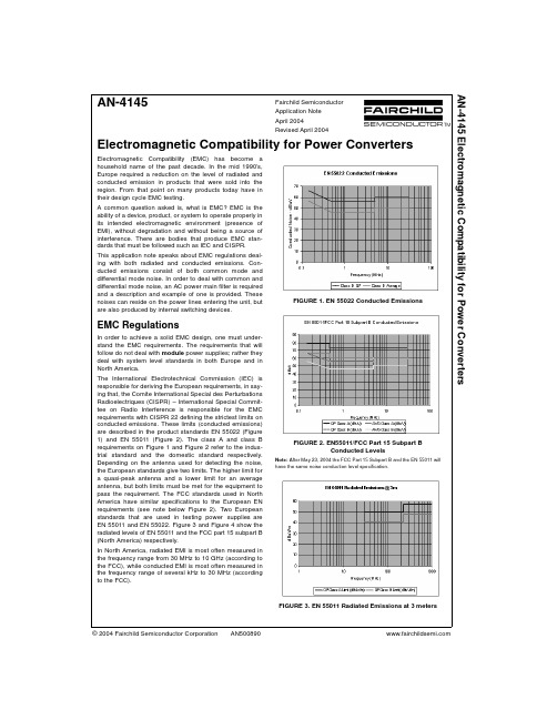
© 2004 Fairchild Semiconductor Corporation Fairchild Semiconductor Application NoteApril 2004Revised April 2004AN-4145 Electromagnetic Compatibility for Power ConvertersAN-4145Electromagnetic Compatibility for Power ConvertersElectromagnetic Compatibility (EMC) has become a household name of the past decade. In the mid 1990’s,Europe required a reduction on the level of radiated and conducted emission in products that were sold into the region. From that point on many products today have in their design cycle EMC testing.A common question asked is, what is EMC? EMC is the ability of a device, product, or system to operate properly in its intended electromagnetic environment (presence of EMI), without degradation and without being a source of interference. There are bodies that produce EMC stan-dards that must be followed such as IEC and CISPR.This application note speaks about EMC regulations deal-ing with both radiated and conducted emissions. Con-ducted emissions consist of both common mode and differential mode noise. In order to deal with common and differential mode noise, an AC power main filter is required and a description and example of one is provided. These noises can reside on the power lines entering the unit, but are also produced by internal switching devices.EMC RegulationsIn order to achieve a solid EMC design, one must under-stand the EMC requirements. The requirements that will follow do not deal with module power supplies; rather they deal with system level standards in both Europe and in North America.The International Electrotechnical Commission (IEC) is responsible for deriving the European requirements, in say-ing that, the Comite International Special des Perturbations Radioelectriques (CISPR) – International Special Commit-tee on Radio Interference is responsible for the EMC requirements with CISPR 22 defining the strictest limits on conducted emissions. These limits (conducted emissions)are described in the product standards EN 55022 (Figure 1) and EN 55011 (Figure 2). The class A and class B requirements on Figure 1 and Figure 2 refer to the indus-trial standard and the domestic standard respectively.Depending on the antenna used for detecting the noise,the European standards give two limits. The higher limit for a quasi-peak antenna and a lower limit for an average antenna, but both limits must be met for the equipment to pass the requirement. The FCC standards used in North America have similar specifications to the European EN requirements (see note below Figure 2). Two European standards that are used in testing power supplies are EN 55011 and EN 55022. Figure 3 and Figure 4 show the radiated levels of EN 55011 and the FCC part 15 subpart B (North America) respectively.In North America, radiated EMI is most often measured in the frequency range from 30 MHz to 10 GHz (according to the FCC), while conducted EMI is most often measured in the frequency range of several kHz to 30 MHz (according to the FCC).FIGURE 1. EN 55022 Conducted EmissionsFIGURE 2. EN55011/FCC Part 15 Subpart BConducted LevelsNote: After May 23, 2004 the FCC Part 15 Subpart B and the EN 55011 will have the same noise conduction level specification.FIGURE 3. EN 55011 Radiated Emissions at 3 meters 2A N -4145EMC Regulations (Continued)FIGURE 4. FCC Part 15 Subpart B Radiated Emissionsat 3 meters The goal here is to develop a system that can comply with some or all of the emissions presented above whether it is a stand alone device or incorporated into a larger system.Common Mode and Differential Mode NoiseThere are two major sources of noise, common mode and differential mode. Common mode noise (Figure 5) comes from common mode current. Common mode energy is common to both lines in a single phase system. This energy travels on all the lines, or wires, in the same direc-tion, and this energy is between all these wires and ground.Because the same level is on both wires at the same time,no attenuation is given by any device between the lines.FIGURE 5. Common Mode NoiseCommon mode noise from common mode current always exists on cables entering the device. One way to minimize these currents is to test the cables early on prototype mod-els (this gives the designer the ability to make any changes necessary before the design is finalized for production) and prior to performing EMC compliance testing. In a lot of cases if the device fails the common-mode current test, it will also fail the radiated emission test. The common mode current can be easily measured by using a high frequency clamp on current probe and a spectrum analyzer. A current probe with a response range of up to 250 MHz should be sufficient.Differential mode noise (Figure 6) is the opposite of com-mon mode noise. This noise is produced by current flowing along either the live or neutral conductor and returning by the other. This produces a noise voltage between the live and neutral conductors.FIGURE 6. Differential Mode NoiseAN-4145AC Power Line Main FilterFIGURE 7. Single Phase AC Line FilterAn example of a single phase AC line filter is shown in Fig-ure 7. Filters of this type are commonly used in reducing both differential and common mode noise from entering and leaving the power supply. The filter in Figure 7 has been broken up into different sections to help better describe its overall function.Note: Both Section A blocks and Section B blocks perform the same func-tion with the only difference being one is for noise entering the device where the other is used for noise exiting the device.BlocksSection AInductors L1/L2 and capacitor C1 represent a differential filter for any noise trying to enter the power supply. Differ-ential mode noise is produced by current flowing along either the line or neutral conductor and returning by the other. The combination of L1 and C1 or L2 and C1 repre-sent a voltage divider. Depending on the frequency of the noise, the capacitor C1 represents a smaller impedance (larger load) to the signal thereby reducing any noise on the line. As an example if the impedance of L1 is 10K and the impedance of C1 is 1K at a particular frequency, the noise passing through the filter would be a tenth of its origi-nal strength or a reduction of 20dB.Section BCapacitors C2 and C3 represent a common mode filter with a reference to ground. Common mode noise manifests itself as a current in phase with the live and neutral conduc-tors and returns via the safety earth. This produces a noise voltage between live/neutral and earth. With all C2, C3, C4,and C5 all being equal, any common mode noise on these lines will be shunted to ground.Note: Section B is not used in medical equipment due to leakage current.Section CSection C of Figure 7 represents the Zorro Inductor (com-mon mode choke) without a reference. The direction of each winding is chosen to give an opposing current flow so any noise present will be cancelled. Magnetic flux caused by common mode current is accumulated, producing impedance, thereby reducing any noise on the line. Since differential mode has currents running in different direc-tions, magnetic flux caused by differential mode current cancels each other, and impedance is not produced thereby having no effect.Note: Capacitors C1 and C6 are X Class capacitors, used to reduce differ-ential noise and are tested to withstand mains voltage. X Class capacitors usually run in the 0.01uF to 2uF range. Capacitors C2 through C5 are Y Class capacitors for common mode noise and are tested to ensure thatthey cannot fail to short circuit (more expensive than X Class). Y Class capacitors are smaller in value usually running between 0.002uF to 0.1uF.AC Power LineFilter Design Example(AD/DC Flyback Converter)Design Requirements:•Transformer turns ratio (a) = 10•Output Impedance (Zs) = 10Ω (load impedance, worst case for maximum output power)•Noise reduction required at 20 kHz = 35dB•Additional headroom for unknown frequency spike = 6dB •AC Line Frequency (Fl) = 60Hz•PWM Switching Frequency (Fs) = 100 kHzTo determine the values of the filter, the output load imped-ance must be recognized. In order to recognize this imped-ance the output load (worst case) must be reflected back to the primary across the transformer using equation 1.whereOn the input side, the filter will be designed for 10 times the line frequency (keeping the filter transparent to both the line and load), thereby resulting in a frequency of 600Hz. In saying this, the cutoff frequency (Fo) must not be below 600Hz. With a noise reduction of 41dB (35dB plus the 6dB of headroom) at 20 kHz, the designer divides 20 kHz by 2and subtracts 12dB from 41dB (see Table 1). Initially a sin-gle inductor will be used to see if this can be accomplished;if not a second series inductor will be needed. A single inductor will give a drop off of 12dB/octave or 40dB/decade. As shown in Table 1, a single inductor is sufficient for this design with the cutoff frequency (Fo) being 1.25kHz (above the minimum 600Hz limit).Zp =Primary Impedance Zs =Secondary Impedancea =Transformer Turns Ratio (Np/Ns) 4A N -4145AC Power Line Filter Design Example (AD/DC Flyback Converter)(Continued)TABLE 1. Input Inductor Determination Now that the cutoff frequency (Fo) is known, the value of the inductor can be created using equation 2.whereUsing Equation 3, one can determine the differential capacitance (Cd) required to complete the differential mode circuit (Section A).whereFor a balanced filter (an inductor on both the live and neu-tral lines), the value is divided by 2, giving 64mH. With the inductance being so large, two inductors will be used to reduce its size. Also an advantage to having more induc-tors is not only to reduce the inductance, but the Q of the filter decreases, thereby decreasing the risk of oscillations.Table 2 represents a second inductor added to the filter giv-ing a 24dB/octave reduction.TABLE 2. Addition of a Second Inductor Using Equation 4 and 5 the subsequent new inductor and capacitor values can be computed.whereAgain, for a balanced filter (an inductor on both the live and neutral lines), the result is divided by 2, giving 16mH.whereThe common mode Zorro inductor is the remaining device to be calculated. The Zorro inductor is calculated the same way in which inductor (L) was, but instead of starting off using the cutoff frequency (Fo), one uses the PWM switch-ing frequency (Fs) (see Table 3) and the same dB loss.Since two differential mode inductors are required, two Zorro inductors will be used to complete the filter.TABLE 3. Zorro Inductor Calculations Frequency (kHz)dB(Limit of Conducted Emissions)2041 (35dB plus 6 dB of headroom)10295172.551.25 (Fo)−7L =Differential InductorZp =Primary Impedance(reflected back from the secondary)Fo =Cutoff Frequency from Table 1L =Differential InductorZp =Primary Impedance(reflected back from the secondary)Frequency (kHz)dB(Limit of Conducted Emissions)2041 (35dB plus 6 dB of headroom)10175 (Fnew)−7Lnew =New Differential InductorZp =Primary Impedance(reflected back from the secondary)Fnew =Cutoff Frequency from Table 2Lnew =New Differential InductorZp =Primary Impedance(reflected back from the secondary)Frequency (kHz)dB(Limit of Conducted Emissions)10041 (35dB plus 6 dB of headroom)501725 (Foz)−7AN-4145AC Power Line Filter Design Example (AD/DC Flyback Converter)(Continued)Using Equations 6 and 7, the Zorro inductance (Lzorro)and Zorro capacitance (Czorro) can be found.wherewhereThe final design is shown in Figure 8.If there are problems at the high frequencies, ferrite beads can be added (ferrite beads act as resistors (50 to 200Ω) at low frequencies and inductors at high ones (30MHz)). If dif-ferential problems occur, increase the Lnew inductors some, or improve the quality of the Cdnew capacitance,they may have too much leakage at the frequency in ques-tion. Common mode problems can be combated by increasing Lzorro inductors.FIGURE 8. Final Filter DesignDesign Guide to Reduce Internal andExternal In Power ConvertersThere are three areas of noise generation in an AC to DC power supply:1.Any noise already present on the AC mains enteringthe power supply unit (common mode/differential mode)2.The switching frequency of the power supply (commonmode)3.The fast switching edges and ringing produced whenthe MOSFET is turned off (common mode)1) AC MainsWith noisy power main lines, an AC power line filter is used. When using an AC power line filter make sure that it is mounted as close as possible to where the AC power line enters the printed circuit board (PCB), see Figure 9.Also the ground connection to the filter should be as short as possible with many vias to the ground plane of the pri-mary side of the power supply.FIGURE 9. Grounding the Common Mode Capacitorsto the Ground Plane In order to reduce common mode and differential mode noise from leaving and entering the unit, an AC power line filter needs to be used. See section on AC Power Line Main Filter.Lzorro =Common Mode InductorZp =Primary Impedance(reflected back from the secondary)Foz =Cutoff Frequency from Table 3Lzorro =Common Mode InductorZp =Primary Impedance(reflected back from the secondary) 6A N -4145Design Guide to Reduce Internal and External In Power Converters(Contin-2) Switching Frequency of the Power SupplyJust like in a system that uses a system clock, many power supplies have a pulse width modulator (PWM) device that operates at a frequency that is used to control the output voltage. So where a system clock needs to be carefully laid out on a PCB, so does the PWM controller.In a flyback, forward or other topology design using a trans-former, it is important to make the trace from the primary winding to the drain of the switching MOSFET (either inter-nal or external) as wide and short as possible (see Figure 10). This reduces the inductance path thereby keeping the ringing to a minimum. A solid ground plane with a minimal number of holes is preferred to ground both the MOSFET and PWM controller too. There should always be a ground running parallel to the trace for current return (if stray capacitance is not a problem), if there still is a noise issue,one can minimize the drain trace capacitance to the trans-former by removing the ground plane from under the trace shown in Figure 10. There are already parasitic capacitors within the MOSFET switch structure that pump current to and from ground. If the ground plane is not removed below the “cross hatched ” trace, then additional current will be passed into the ground causing more common mode con-ducted noise.FIGURE 10. Reducing Drain Trace CapacitanceNote: Especially at higher frequencies, example 500kHzThe source of the MOSFET doing the switching must have a solid connection to the primary side ground plane. In order to accomplish this make a large landing pad for the ground terminal so that a proper number of vias (depend-ing on the sinking current) can be used to make a solid connection to the ground plane, see Figure 11.FIGURE 11. Connecting the Source of an Internal MOSFET to the Ground Planewith a Sufficient Number of Vias 3) PWM Switching Edges and Subsequent Ringing Figure 12 shows a Resistor Capacitor Diode (RCD) cir-cuitry (R1, C1, and D1) that serves two purposes; firstly C1shows down the collector voltage rise time (smoothening,reducing radiated EMI) when Q1 is turned off and secondly,it maintains the input voltage to 2V CC as not to exceed the breakdown voltage of the switching MOSFET. In making C1 large enough, the rising collector voltage and falling col-lector current intersect so low down that the transistor dissi-pation is decreased significantly.The ringing circuitry (Figure 12 (C2 and R2)) is also impor-tant and used to reduce the ringing of the primary side of the transformer caused when the MOSFET relaxes to the input voltage of the power supply, shown below in Figure 13 and Figure 14.FIGURE 12. RCD Snubber and RC Ringing CircuitryAN-4145Design Guide to Reduce Internal and External In Power Converters (Contin-FIGURE 13. Primary Voltage Waveform Without Ringing Circuitry (C2, R2)FIGURE 14. Primary Voltage Waveform with Ringing Circuitry (C2, R2)As a first pass, one method of determining the values for C2 and R2 is as follows:1.Determine the frequency of the ringing waveform andcalculate the period.2.Multiply the period, determined in Step 1, by 5.3.Assume a value for the resistor (usually less than100R).4.Calculate the size of the capacitor by dividing the num-ber obtained in Step 2 by the size of the resistor inStep 3.Note: The advantage of using the resistor R2 and the capacitor C2 network is that it reduces the ringing as shown in Figure 11, but the disadvantage is that the high frequency ripple passing through capacitor C2 gets dissipated as heat in resistor R2. If noise reduction is more important than efficiency then proceed, otherwise efficiency will drop off some.8A N -4145 E l e c t r o m a g n e t i c C o m p a t i b i l i t y f o r P o w e r C o n v e r t e r sPrinted Circuit Board Guidelines1.Take the time to place and orient the components prop-erly.2.If heat sinks are used, make sure they are grounded.3. A component shield maybe required.mon mode capacitors should have low ESR val-ues as well as maintain a short lead length to the ground place.5.If a snubber circuit is being used across the trans-former to slow down the rise time of the MOSFET switch turning off, make sure that the trace lengths from the drain and two primary transformer pins are short. If possible place the snubber circuitry between the two primary pins.6.avoid slots in the ground and power (if used) planes7.Under 50 MHz (don ’t forget to consider the harmonicsof the PWM controller) traditional decoupling methods are effective. Use one or two decoupling capacitors (often 0.1 or 0.01 uF) placed close to the IC power and ground pins. Consider the loop area formed between the decoupling capacitor and the IC, and place the capacitor for minimum loop area.8.Keep ground runs as short as possible and as thickand large as possible.9.Avoid sharp corners on traces.10.Try to group all noisy component in the same area justin case shielding is e multi-layer printed circuit board if possible.Safety Dealing with Medical EquipmentCommon mode noise is a problem for sensitive equipment such as those in the medical field. If a device touches a patient, the total system leakage is limited to 100uA. This means that most power supply designers want to restrict this leakage current 20 to 40uA. In order to meet this strin-gent requirement, common mode filters with capacitors to ground are not used. Using common mode chokes, feed through capacitors (high frequency noise is shunted to the chassis ground instead of signal ground) to ground and adding a transformer or isolating the power supply lines into the power supply reduces these common mode con-ducted emission pulses. Safety standard: IEC950/UL1950class II is used in medical equipment.ConclusionEMC is an important stage of system design today and will become more stringent as time moves on. One must keep in mind that when switching occurs, so does noise whether it be conducted or radiated noise. This application note spoke about board level techniques to reduce noise, if more noise reduction is required, especially on the radia-tion side, conductive enclosures are an option. There is additional cost with all that is added so as a design engi-neer, standard compliance, safety compliance, and cost all play an important role in the final product.References:EMI Filter Design (1996)Richard Lee OzenbaughFairchild does not assume any responsibility for use of any circuitry described, no circuit patent licenses are implied and Fairchild reserves the right at any time without notice to change said circuitry and specifications.LIFE SUPPORT POLICYFAIRCHILD ’S PRODUCTS ARE NOT AUTHORIZED FOR USE AS CRITICAL COMPONENTS IN LIFE SUPPORT DEVICES OR SYSTEMS WITHOUT THE EXPRESS WRITTEN APPROVAL OF THE PRESIDENT OF FAIRCHILD SEMICONDUCTOR CORPORATION. As used herein:1.Life support devices or systems are devices or systems which, (a) are intended for surgical implant into the body, or (b) support or sustain life, and (c) whose failure to perform when properly used in accordance with instructions for use provided in the labeling, can be rea-sonably expected to result in a significant injury to the user. 2. A critical component in any component of a life support device or system whose failure to perform can be rea-sonably expected to cause the failure of the life support device or system, or to affect its safety or effectiveness.。
X电容与Y电容容量的计算
120
PI-1622-111695
120
AN-15
Safety is a vital issue which determines EMI filter component selection, the transformer reinforced insulation system, and PC board primary to secondary spacing. In fact, safety is an integral part of the power supply/EMI filter design and is difficult to discuss as a separate issue. Throughout this application note, design guidance will also be presented for meeting safety requirements in TOPSwitch power supplies.
反激的典型波形
反激变换器的例子Analysis of basic waveforms基本波形分析The analysis of the basic waveforms will be done on a simula ted example of a flyback converter operating in discontinuous cond uction mode. Typical drain-source voltage waveform of the primary side switch is shown in Fig. 16.在电感电流断续模式下运行的反激变换器的典型一次侧漏源极开关电压波形见图16。
Fig. 16 Typical drain-source voltage of the MOSFET in a flyback 图16反激变换器的典型漏源极电压These drain-source voltage waveforms can be theoretically distin guished into typical elements. Different physical phenomena influence the waveform at given time interval. Fig. 17 and Tab. 4 demo nstrate the main elements of the voltage waveform. The superposit ion of all these elements results in a typical drain-source voltage s hown in Fig. 16.这些漏源极电压波形能用典型的理论来描述。
各个时间段有不同物理现象影响这些波形。
图17和平台4描述了电压波形的主要原理。
把这些原理按时序整合呈现出图16所示的典型漏源极电压。
电磁干扰开关电源中英文对照外文翻译文献
(文档含英文原文和中文翻译)中英文翻译外文资料(原文)Modeling, Simulation, and Reduction of Conducted Electromagnetic Interference Due to a PWM Buck Type Switching Power Supply IAbstract:Undesired generation of radiated or conducted energy in electrical systems is called Electromagnetic Interference (EMI). High speed switching frequency in power electronics converters especially in switching power supplies improves efficiency but leads to EMI. Different kind of conducted interference, EMI regulations and conducted EMI measurement are introduced in this paper. Compliancy with national or international regulation is called Electromagnetic Compatibility (EMC). Power electronic systems producers must regard EMC. Modeling and simulation is the first step of EMC evaluation. EMI simulation results due to a PWM Buck type switching power supply are presented in this paper. To improve EMC, some techniques are introduced and their effectiveness proved by simulation.Index Terms:Conducted, EMC, EMI, LISN, Switching SupplyI. INTRODUCTIONFAST semiconductors make it possible to have high speed and high frequency switching in power electronics []1. High speed switching causes weight and volume reduction of equipment, but some unwanted effects such as radio frequency interference appeared []2. Compliance with electromagnetic compatibility (EMC) regulations is necessary for producers to present their products to the markets. It is important to take EMC aspects already in design phase []3. Modeling and simulation is the most effective tool to analyze EMC consideration before developing theproducts. A lot of the previous studies concerned the low frequency analysis of power electronics components []4[]5. Different types of power electronics converters are capable to be considered as source of EMI. They could propagate the EMI in both radiated and conducted forms. Line Impedance Stabilization Network (LISN) is required for measurement and calculation of conducted interference level []6. Interference spectrum at the output of LISN is introduced as the EMC evaluation criterion []7[]8. National or international regulations are the references for the evaluation of equipment in point of view of EMC []7[]8. II. SOURCE, PATH AND VICTIM OF EMIUndesired voltage or current is called interference and their cause is called interference source. In this paper a high-speed switching power supply is the source of interference.Interference propagated by radiation in area around of an interference source or by conduction through common cabling or wiring connections. In this study conducted emission is considered only. Equipment such as computers, receivers, amplifiers, industrial controllers, etc that are exposed to interference corruption are called victims. The common connections of elements, source lines and cabling provide paths for conducted noise or interference. Electromagnetic conducted interference has two components as differential mode and common mode []9.A. Differential mode conducted interferenceThis mode is related to the noise that is imposed between different lines of a test circuit by a noise source. Related current path is shown in Fig. 1 []9. The interference source, path impedances, differential mode current and load impedance are also shown in Fig. 1.B. Common mode conducted interferenceCommon mode noise or interference could appear and impose between the lines, cables or connections and common ground. Any leakage current between load and common ground could be modeled by interference voltage source.Fig. 2 demonstrates the common mode interference source, commonmode currents Icm1 and Icm2and the related current paths[]9.The powerelectronics converters perform as noise source between lines of the supply network. In this study differential mode of conducted interferenceis particularly important and discussion will be continued considering this mode only.III. ELECTROMAGNETIC COMPATIBILITY REGULATIONSApplication of electrical equipment especially static power electronic converters in different equipment is increasing more and more. As mentioned before, power electronics converters are considered as an important source of electromagnetic interference and have corrupting effects on the electric networks []2. High level of pollution resulting from various disturbances reduces the quality of power in electric networks. On the other side some residential, commercial and especially medical consumers are so sensitive to power system disturbances including voltage and frequency variations. The best solution to reduce corruption and improve power quality is complying national or international EMCregulations. CISPR, IEC, FCC and VDE are among the most famous organizations from Europe, USA and Germany who are responsible for determining and publishing the most important EMC regulations. IEC and VDE requirement and limitations on conducted emission are shown in Fig. 3 and Fig. 4 []7[]9.For different groups of consumers different classes of regulations could be complied. Class A for common consumers and class B with more hard limitations for special consumers are separated in Fig. 3 and Fig. 4. Frequency range of limitation is different for IEC and VDE that are 150 kHz up to 30 MHz and 10 kHz up to 30 MHz respectively. Compliance of regulations is evaluated by comparison of measured or calculated conducted interference level in the mentioned frequency range with the stated requirements in regulations. In united European community compliance of regulation is mandatory and products must have certified label to show covering of requirements []8.IV. ELECTROMAGNETIC CONDUCTED INTERFERENCE MEASUREMENTA. Line Impedance Stabilization Network (LISN)1-Providing a low impedance path to transfer power from source to power electronics converter and load.2-Providing a low impedance path from interference source, here power electronics converter, to measurement port.Variation of LISN impedance versus frequency with the mentioned topology is presented in Fig. 7. LISN has stabilized impedance in the range of conducted EMI measurement []7.Variation of level of signal at the output of LISN versus frequency is the spectrum of interference. The electromagnetic compatibility of a system can be evaluated by comparison of its interference spectrum with the standard limitations. The level of signal at the output of LISN in frequency range 10 kHz up to 30 MHz or 150 kHz up to 30 MHz is criterion of compatibility and should be under the standard limitations. In practical situations, the LISN output is connected to a spectrum analyzer and interference measurement is carried out. But for modeling and simulation purposes, the LISN output spectrum is calculated using appropriate software.外文资料(译文)基于压降型PWM开关电源的建模、仿真和减少传导性电磁干扰摘要:电子设备之中杂乱的辐射或者能量叫做电磁干扰(EMI)。
沿电源线的瞬态传导抗扰英文缩写
沿电源线的瞬态传导抗扰英文缩写Transient Conducted Immunity along Power Lines.Transient conducted immunity along power lines is a crucial aspect of electrical and electronic equipment reliability and safety. It refers to the ability of equipment to withstand temporary voltage or current disturbances that may occur on the power line, without experiencing damage or malfunction. These disturbances can be caused by various sources such as lightning strikes, switching transients, electrostatic discharges, and other electromagnetic interference (EMI) sources.Transient conducted immunity is an important consideration in the design and testing of electrical and electronic equipment. Equipment that fails to meet the required transient conducted immunity standards may experience performance degradation, malfunction, or even permanent damage when subjected to these disturbances. Therefore, it is essential to ensure that equipment isdesigned and tested to withstand the transient conducted immunity levels specified in relevant standards and regulations.Transient conducted immunity standards and testing methods vary depending on the type of equipment and its intended application. For example, the International Electrotechnical Commission (IEC) has published a series of standards that specify transient conducted immunity requirements for different types of equipment. These standards include IEC 61000-4-5, which covers the immunity of electrical and electronic equipment to transient disturbances induced by switching on and off of inductive loads connected to the power lines.To ensure compliance with transient conducted immunity standards, equipment manufacturers must conduct rigorous testing during the design and development process. Testing typically involves exposing the equipment to controlled transient disturbances that simulate real-world conditions. The equipment is then evaluated to determine if it can operate normally or recover from the disturbance withoutexperiencing damage or malfunction.In addition to meeting transient conducted immunity standards, equipment manufacturers must also consider other factors that can affect equipment reliability and safety. For example, equipment should be designed to withstand voltage surges and spikes that may occur on the power line due to lightning strikes or other EMI sources. Manufacturers may incorporate surge protection devices, such as varistors or gas discharge tubes, to limit the voltage across sensitive components and prevent damage.Furthermore, equipment should be designed to minimize the generation of EMI itself. This can be achieved through the use of shielding, filtering, and grounding techniques. Shielding can reduce the coupling of EMI signals into sensitive circuits, while filtering can remove EMI components from the power line before they reach the equipment. Grounding ensures that any EMI signals generated by the equipment are conducted to the power line or earth ground, preventing them from interfering with othercircuits or equipment.In conclusion, transient conducted immunity along power lines is a crucial aspect of electrical and electronic equipment reliability and safety. Manufacturers must ensure that their equipment is designed and tested to meet the transient conducted immunity standards specified in relevant regulations and standards. Additionally, they should consider other factors such as voltage surge protection and EMI reduction techniques to further enhance equipment reliability and safety. By doing so, they can ensure that their equipment can withstand the transient disturbances that may occur on the power line and continue to operate effectively and safely.。
- 1、下载文档前请自行甄别文档内容的完整性,平台不提供额外的编辑、内容补充、找答案等附加服务。
- 2、"仅部分预览"的文档,不可在线预览部分如存在完整性等问题,可反馈申请退款(可完整预览的文档不适用该条件!)。
- 3、如文档侵犯您的权益,请联系客服反馈,我们会尽快为您处理(人工客服工作时间:9:00-18:30)。
I.
INTRODUCTION
As the power electronic technology develops, the conducted EMI of switching power supply(SMPS) becomes a big problem. The governments proposes strict rules and standards to ensure the EMC target of products. Usually a EMC test may cost a lot of time and money, which disturbs designers a lot. So, this paper try to use simulation analysis in time domain to forecast the conducted EMI in flyback converters. Based on the simulation result, the designer can recompose the converter which can bring a good result in EMC test before the product come into the market. That will help the designer to put out product faster and cost less money.
1794
978-1-4577-2088-8/11/$26.00 ©2012 IEEE
current [3]. Fig. 2 shows the way DM noise go through the converter to the LISN.
24 VDC
50μH
1uF
0.1uF
50μH
0.1uF 1uF
Li Longtao, Wang Lixin, Lv Chao, Sun Chao
School of Electrical Engineering and Automation Harbin Institute of Technology Harbin, China lilongtaohit@
Unlike CM noise current ICM, the DM noise current IDM which is usually introduced by the secondary power diode’s pulsating
The authors express their great thanks to the support of The National Natural Science Foundation of China (51077016)
and goes through the parasitic capacitance Cp to the ground, plays a leading role in a range of 5MHz to 30MHz in
conducted EMI [2]. Cp represents the total of parasitic capacitance between the converter to the ground, including
MOSFET and heat sink’s parasitic capacitance Cp , the output line’s parasitic capacitance CL. Fig. 1 shows the way the CM noise current goes through the converter to the ground. Unlike
Abstract—The measure of conducted EMI needs strict environment and expensive instruments, most of the designers don’t have this condition. So, there are demands for economic forecast of conducted EMI before the product being tested by the government. This paper tries a simulation method to forecast the conducted EMI of a flyback converter. First, this paper analyses the mechanism of conducted EMI which shows the transformer and MOSFET is key point of conducted EMI. The voltage pulsating of primary MOSFET is a source of CM noise (common mode EMI). The transformer and its’ parasitic parameters are the coupling channels for conducted EMI from primary to secondary. The DM noise (differential mode EMI) is introduced by current pulsating of the diode in the secondary, which refluxes through the circuit of converter. Considering the structure of the flyback transformers, especially the effects of shielding layer on conducted EMI, this paper proposes a module of transformer with shielding layer and a formula of coupling capacitance between shielding layer and the windings. After discussing the parasitic capacitance of heat sink, the module of power MOSFET is built. Use Q3D software to extract the parasitic parameters of PCB board and put the whole module into SABER to simulate the conducted EMI. Finally, the simulated result is compared with a measured result which shows the simulation result is credible, and proves the simulation method is a economic and fast way to forecast conducted EMI.
VNபைடு நூலகம்
50Ω
VL
50Ω
Idm
Cps
I dm1
Q
Idm
DC
RL
I dm 2
LISN Figure 2. the route of DM noise
Bobbin
Shielding layer Figure 3. structure of transformer
Shielding layer
II. MODULING AND SIMULATION
equipment must use LISN( line impendence stabilization network ) to obtain the conducted EMI and insulate the interference from the power supply. Fig. 1 shows the noise current come through the LISN, form the noise voltage VL and VN on the 50 Ω resistances. The CM noise voltage VCM and the DM noise voltage VDM can be calculated in the next two equation [1].
2012 IEEE 7th International Power Electronics and Motion Control Conference - ECCE Asia June 2-5, 2012, Harbin, China
A Simulation of Conducted EMI in Flyback Converters
VC=M (VL + VN ) / 2
(1)
24 VDC
VD=M
50μH
1uF
0.1uF
50μH
(VL −VN ) / 2
Icm
Cps
I cm1
0.1uF
1uFVN
VL
Q
50Ω
50Ω
Icm
LISN
(2)
DC
RL
I cm 2
Cp
Cl
Figure 1. The route of CM noise
The CM noise current ICM, is introduced by voltage pulsation caused by the power MOSFET’s switching action,