半导体集成电路原理与设计—第三章答辩
半导体物理与器件 尼曼 第四版第三章课后答案
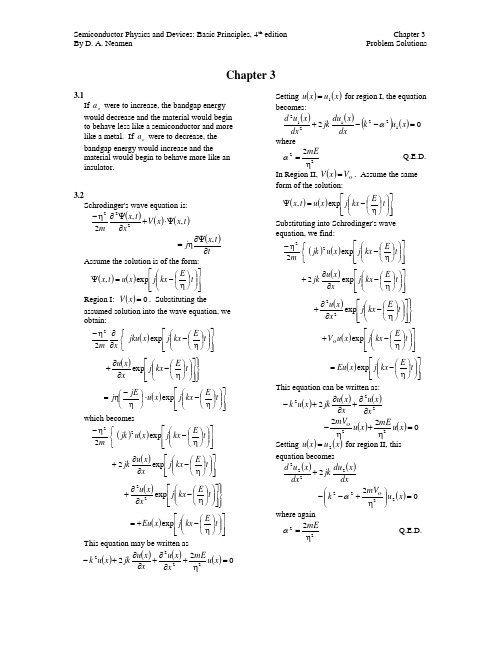
Chapter 33.1If o a were to increase, the bandgap energy would decrease and the material would begin to behave less like a semiconductor and more like a metal. If o a were to decrease, the bandgap energy would increase and thematerial would begin to behave more like an insulator._______________________________________ 3.2Schrodinger's wave equation is:()()()t x x V xt x m ,,2222ψ⋅+∂ψ∂- ()tt x j ∂ψ∂=, Assume the solution is of the form:()()⎥⎥⎦⎤⎢⎢⎣⎡⎪⎪⎭⎫ ⎝⎛⎪⎭⎫ ⎝⎛-=ψt E kx j x u t x exp , Region I: ()0=x V . Substituting theassumed solution into the wave equation, we obtain:()⎥⎥⎦⎤⎢⎢⎣⎡⎪⎪⎭⎫ ⎝⎛⎪⎭⎫ ⎝⎛-⎩⎨⎧∂∂-t E kx j x jku x m exp 22 ()⎪⎭⎪⎬⎫⎥⎥⎦⎤⎢⎢⎣⎡⎪⎪⎭⎫ ⎝⎛⎪⎭⎫ ⎝⎛-∂∂+t E kx j x x u exp ()⎥⎥⎦⎤⎢⎢⎣⎡⎪⎪⎭⎫ ⎝⎛⎪⎭⎫ ⎝⎛-⋅⎪⎭⎫ ⎝⎛-=t E kx j x u jE j exp which becomes()()⎥⎥⎦⎤⎢⎢⎣⎡⎪⎪⎭⎫ ⎝⎛⎪⎭⎫ ⎝⎛-⎩⎨⎧-t E kx j x u jk m exp 222 ()⎥⎥⎦⎤⎢⎢⎣⎡⎪⎪⎭⎫ ⎝⎛⎪⎭⎫ ⎝⎛-∂∂+t E kx j x x u jkexp 2 ()⎪⎭⎪⎬⎫⎥⎥⎦⎤⎢⎢⎣⎡⎪⎪⎭⎫ ⎝⎛⎪⎭⎫ ⎝⎛-∂∂+t E kx j x x u exp 22 ()⎥⎥⎦⎤⎢⎢⎣⎡⎪⎪⎭⎫ ⎝⎛⎪⎭⎫ ⎝⎛-+=t E kx j x Eu exp This equation may be written as()()()()0222222=+∂∂+∂∂+-x u mE x x u x x u jk x u kSetting ()()x u x u 1= for region I, the equation becomes:()()()()021221212=--+x u k dx x du jk dxx u d α where222mE=α Q.E.D.In Region II, ()O V x V =. Assume the same form of the solution:()()⎥⎥⎦⎤⎢⎢⎣⎡⎪⎪⎭⎫ ⎝⎛⎪⎭⎫ ⎝⎛-=ψt E kx j x u t x exp , Substituting into Schrodinger's wave equation, we find:()()⎥⎥⎦⎤⎢⎢⎣⎡⎪⎪⎭⎫ ⎝⎛⎪⎭⎫ ⎝⎛-⎩⎨⎧-t E kx j x u jk m exp 222 ()⎥⎥⎦⎤⎢⎢⎣⎡⎪⎪⎭⎫ ⎝⎛⎪⎭⎫ ⎝⎛-∂∂+t E kx j x x u jkexp 2 ()⎪⎭⎪⎬⎫⎥⎥⎦⎤⎢⎢⎣⎡⎪⎪⎭⎫ ⎝⎛⎪⎭⎫ ⎝⎛-∂∂+t E kx j x x u exp 22 ()⎥⎥⎦⎤⎢⎢⎣⎡⎪⎪⎭⎫ ⎝⎛⎪⎭⎫ ⎝⎛-+t E kx j x u V O exp ()⎥⎥⎦⎤⎢⎢⎣⎡⎪⎪⎭⎫ ⎝⎛⎪⎭⎫ ⎝⎛-=t E kx j x Eu exp This equation can be written as:()()()2222x x u x x u jk x u k ∂∂+∂∂+- ()()02222=+-x u mEx u mV OSetting ()()x u x u 2= for region II, this equation becomes()()dx x du jk dxx u d 22222+ ()022222=⎪⎪⎭⎫ ⎝⎛+--x u mV k O α where again222mE=α Q.E.D._______________________________________3.3We have ()()()()021221212=--+x u k dx x du jk dx x u d α Assume the solution is of the form:()()[]x k j A x u -=αexp 1 ()[]x k j B +-+αexpThe first derivative is()()()[]x k j A k j dxx du --=ααexp 1()()[]x k j B k j +-+-ααexp and the second derivative becomes()()[]()[]xk j A k j dx x u d --=ααexp 2212 ()[]()[]x k j B k j +-++ααexp 2Substituting these equations into thedifferential equation, we find ()()[]x k j A k ---ααexp 2()()[]x k j B k +-+-ααexp 2(){()[]x k j A k j jk --+ααexp 2()()[]}x k j B k j +-+-ααexp ()()[]{x k j A k ---ααexp 22 ()[]}0exp =+-+x k j B α Combining terms, we obtain()()()[]222222αααα----+--k k k k k ()[]x k j A -⨯αexp()()()[]222222αααα--++++-+k k k k k ()[]0exp =+-⨯x k j B α We find that00= Q.E.D. For the differential equation in ()x u 2 and the proposed solution, the procedure is exactly the same as above._______________________________________ 3.4We have the solutions ()()[]x k j A x u -=αexp 1()[]x k j B +-+αexp for a x <<0 and()()[]x k j C x u -=βexp 2()[]x k j D +-+βexp for 0<<-x b .The first boundary condition is ()()0021u u =which yields 0=--+D C B AThe second boundary condition is 0201===x x dx du dx duwhich yields()()()C k B k A k --+--βαα ()0=++D k β The third boundary condition is ()()b u a u -=21 which yields()[]()[]a k j B a k j A +-+-ααexp exp ()()[]b k j C --=βexp ()()[]b k j D -+-+βexp and can be written as ()[]()[]a k j B a k j A +-+-ααexp exp ()[]b k j C ---βexp()[]0exp =+-b k j D βThe fourth boundary condition isbx a x dx dudx du -===21 which yields()()[]a k j A k j --ααexp()()[]a k j B k j +-+-ααexp ()()()[]b k j C k j ---=ββexp()()()[]b k j D k j -+-+-ββexp and can be written as ()()[]a k j A k --ααexp()()[]a k j B k +-+-ααexp()()[]b k j C k ----ββexp()()[]0exp =+++b k j D k ββ_______________________________________ 3.5(b) (i) First point: πα=aSecond point: By trial and error, πα729.1=a (ii) First point: πα2=aSecond point: By trial and error, πα617.2=a_______________________________________3.6 (b) (i) First point: πα=a Second point: By trial and error,πα515.1=a (ii) First point: πα2=aSecond point: By trial and error, πα375.2=a_______________________________________ 3.7 ka a a a P cos cos sin =+'ααα Let y ka =, x a =αThen y x x x P cos cos sin =+' Consider dy d of this function.()[]{}y x x x P dy d sin cos sin 1-=+⋅'- We find()()()⎭⎬⎫⎩⎨⎧⋅+⋅-'--dy dx x x dy dx x x P cos sin 112y dydxx sin sin -=- Theny x x x x x P dy dx sin sin cos sin 12-=⎭⎬⎫⎩⎨⎧-⎥⎦⎤⎢⎣⎡+-'For πn ka y ==, ...,2,1,0=n 0sin =⇒y So that, in general,()()dk d ka d a d dy dxαα===0 And 22 mE=α Sodk dEm mE dk d ⎪⎭⎫ ⎝⎛⎪⎭⎫ ⎝⎛=-22/122221 α This implies thatdk dE dk d ==0α for an k π= _______________________________________ 3.8 (a) πα=a 1 π=⋅a E m o 212 ()()()()2103123422221102.41011.9210054.12---⨯⨯⨯==ππa m E o 19104114.3-⨯=J From Problem 3.5πα729.12=a π729.1222=⋅a E m o ()()()()2103123422102.41011.9210054.1729.1---⨯⨯⨯=πE 18100198.1-⨯=J 12E E E -=∆1918104114.3100198.1--⨯-⨯=19107868.6-⨯=Jor 24.4106.1107868.61919=⨯⨯=∆--E eV(b) πα23=aπ2223=⋅a E m o()()()()2103123423102.41011.9210054.12---⨯⨯⨯=πE18103646.1-⨯=J From Problem 3.5, πα617.24=aπ617.2224=⋅a E m o()()()()2103123424102.41011.9210054.1617.2---⨯⨯⨯=πE18103364.2-⨯=J 34E E E -=∆1818103646.1103364.2--⨯-⨯= 1910718.9-⨯=Jor 07.6106.110718.91919=⨯⨯=∆--E eV_______________________________________3.9 (a) At π=ka , πα=a 1π=⋅a E m o 212()()()()2103123421102.41011.9210054.1---⨯⨯⨯=πE19104114.3-⨯=JAt 0=ka , By trial and error, πα859.0=a o ()()()()210312342102.41011.9210054.1859.0---⨯⨯⨯=πoE19105172.2-⨯=J o E E E -=∆11919105172.2104114.3--⨯-⨯= 2010942.8-⨯=Jor 559.0106.110942.81920=⨯⨯=∆--E eV (b) At π2=ka , πα23=aπ2223=⋅a E m o()()()()2103123423102.41011.9210054.12---⨯⨯⨯=πE18103646.1-⨯=JAt π=ka . From Problem 3.5, πα729.12=aπ729.1222=⋅a E m o()()()()2103123422102.41011.9210054.1729.1---⨯⨯⨯=πE18100198.1-⨯=J23E E E -=∆1818100198.1103646.1--⨯-⨯= 19104474.3-⨯=Jor 15.2106.1104474.31919=⨯⨯=∆--E eV_______________________________________3.10 (a) πα=a 1π=⋅a E m o 212()()()()2103123421102.41011.9210054.1---⨯⨯⨯=πE19104114.3-⨯=JFrom Problem 3.6, πα515.12=aπ515.1222=⋅a E m o()()()()2103123422102.41011.9210054.1515.1---⨯⨯⨯=πE1910830.7-⨯=J 12E E E -=∆1919104114.310830.7--⨯-⨯= 19104186.4-⨯=Jor 76.2106.1104186.41919=⨯⨯=∆--E eV (b) πα23=aπ2223=⋅a E m o()()()()2103123423102.41011.9210054.12---⨯⨯⨯=πE18103646.1-⨯=JFrom Problem 3.6, πα375.24=aπ375.2224=⋅a E m o()()()()2103123424102.41011.9210054.1375.2---⨯⨯⨯=πE18109242.1-⨯=J 34E E E -=∆1818103646.1109242.1--⨯-⨯= 1910597.5-⨯=Jor 50.3106.110597.51919=⨯⨯=∆--E eV_____________________________________3.11 (a) At π=ka , πα=a 1π=⋅a E m o 212()()()()2103123421102.41011.9210054.1---⨯⨯⨯=πE19104114.3-⨯=JAt 0=ka , By trial and error, πα727.0=a oπ727.022=⋅a E m o o()()()()210312342102.41011.9210054.1727.0---⨯⨯⨯=πo E19108030.1-⨯=Jo E E E -=∆11919108030.1104114.3--⨯-⨯= 19106084.1-⨯=Jor 005.1106.1106084.11919=⨯⨯=∆--E eV (b) At π2=ka , πα23=aπ2223=⋅a E m o()()()()2103123423102.41011.9210054.12---⨯⨯⨯=πE18103646.1-⨯=JAt π=ka , From Problem 3.6,πα515.12=aπ515.1222=⋅a E m o()()()()2103423422102.41011.9210054.1515.1---⨯⨯⨯=πE1910830.7-⨯=J23E E E -=∆191810830.7103646.1--⨯-⨯= 1910816.5-⨯=Jor 635.3106.110816.51919=⨯⨯=∆--E eV_______________________________________3.12For 100=T K, ()()⇒+⨯-=-1006361001073.4170.124gE164.1=g E eV200=T K, 147.1=g E eV 300=T K, 125.1=g E eV 400=T K, 097.1=g E eV 500=T K, 066.1=g E eV 600=T K, 032.1=g E eV_______________________________________3.13The effective mass is given by1222*1-⎪⎪⎭⎫⎝⎛⋅=dk E d mWe have()()B curve dkE d A curve dk E d 2222> so that ()()B curve m A curve m **<_______________________________________ 3.14The effective mass for a hole is given by1222*1-⎪⎪⎭⎫ ⎝⎛⋅=dk E d m p We have that()()B curve dkEd A curve dk E d 2222> so that ()()B curve m A curve m p p **<_______________________________________ 3.15Points A,B: ⇒<0dk dEvelocity in -x directionPoints C,D: ⇒>0dk dEvelocity in +x directionPoints A,D: ⇒<022dk Ednegative effective massPoints B,C: ⇒>022dkEd positive effective mass _______________________________________3.16 For A: 2k C E i = At 101008.0+⨯=k m 1-, 05.0=E eV Or ()()2119108106.105.0--⨯=⨯=E J So ()2101211008.0108⨯=⨯-C3811025.1-⨯=⇒CNow ()()38234121025.1210054.12--*⨯⨯==C m 311044.4-⨯=kgor o m m ⋅⨯⨯=--*31311011.9104437.4o m m 488.0=* For B: 2k C E i =At 101008.0+⨯=k m 1-, 5.0=E eV Or ()()2019108106.15.0--⨯=⨯=E JSo ()2101201008.0108⨯=⨯-C 3711025.1-⨯=⇒CNow ()()37234121025.1210054.12--*⨯⨯==C m 321044.4-⨯=kg or o m m ⋅⨯⨯=--*31321011.9104437.4o m m 0488.0=*_______________________________________ 3.17For A: 22k C E E -=-υ()()()2102191008.0106.1025.0⨯-=⨯--C 3921025.6-⨯=⇒C()()39234221025.6210054.12--*⨯⨯-=-=C m31108873.8-⨯-=kgor o m m ⋅⨯⨯-=--*31311011.9108873.8o m m 976.0--=* For B: 22k C E E -=-υ()()()2102191008.0106.13.0⨯-=⨯--C 382105.7-⨯=⇒C()()3823422105.7210054.12--*⨯⨯-=-=C m3210406.7-⨯-=kgor o m m ⋅⨯⨯-=--*31321011.910406.7o m m 0813.0-=*_______________________________________ 3.18(a) (i) νh E =or ()()341910625.6106.142.1--⨯⨯==h E ν1410429.3⨯=Hz(ii) 141010429.3103⨯⨯===νλc E hc 51075.8-⨯=cm 875=nm(b) (i) ()()341910625.6106.112.1--⨯⨯==h E ν1410705.2⨯=Hz(ii) 141010705.2103⨯⨯==νλc410109.1-⨯=cm 1109=nm_______________________________________ 3.19(c) Curve A: Effective mass is a constantCurve B: Effective mass is positive around 0=k , and is negativearound 2π±=k ._______________________________________ 3.20()[]O O k k E E E --=αcos 1 Then()()()[]O k k E dkdE ---=ααsin 1()[]O k k E -+=ααsin 1 and()[]O k k E dk E d -=ααcos 2122Then 221222*11 αE dk E d m o k k =⋅== or 212*αE m = _______________________________________ 3.21(a) ()[]3/123/24l t dn m m m =* ()()[]3/123/264.1082.04o o m m = o dn m m 56.0=*(b) oo l t cn m m m m m 64.11082.02123+=+=* oo m m 6098.039.24+= o cn m m 12.0=*_______________________________________3.22(a) ()()[]3/22/32/3lh hh dp m m m +=*()()[]3/22/32/3082.045.0o o m m += []om ⋅+=3/202348.030187.0o dp m m 473.0=*(b) ()()()()2/12/12/32/3lh hh lh hh cpm m m m m ++=*()()()()om ⋅++=2/12/12/32/3082.045.0082.045.0 o cp m m 34.0=*_______________________________________ 3.23For the 3-dimensional infinite potential well, ()0=x V when a x <<0, a y <<0, and a z <<0. In this region, the wave equation is:()()()222222,,,,,,z z y x y z y x x z y x ∂∂+∂∂+∂∂ψψψ()0,,22=+z y x mEψ Use separation of variables technique, so let ()()()()z Z y Y x X z y x =,,ψSubstituting into the wave equation, we have222222z ZXY y Y XZ x X YZ ∂∂+∂∂+∂∂ 022=⋅+XYZ mEDividing by XYZ , we obtain 021*********=+∂∂⋅+∂∂⋅+∂∂⋅ mEz Z Z y Y Y x X XLet 01222222=+∂∂⇒-=∂∂⋅X k x X k x X X x x The solution is of the form:()x k B x k A x X x x cos sin += Since ()0,,=z y x ψ at 0=x , then ()00=X so that 0=B . Also, ()0,,=z y x ψ at a x =, so that()0=a X . Then πx x n a k = where ...,3,2,1=x nSimilarly, we have 2221y k y Y Y -=∂∂⋅ and 2221z k z Z Z -=∂∂⋅ From the boundary conditions, we find πy y n a k = and πz z n a k =where...,3,2,1=y n and ...,3,2,1=z n From the wave equation, we can write022222=+---mE k k k z y xThe energy can be written as()222222⎪⎭⎫⎝⎛++==a n n n m E E z y x n n n z y x π _______________________________________ 3.24The total number of quantum states in the 3-dimensional potential well is given (in k-space) by()332a dk k dk k g T ⋅=ππ where222 mEk =We can then writemEk 2=Taking the differential, we obtaindE E mdE E m dk ⋅⋅=⋅⋅⋅⋅=2112121 Substituting these expressions into the density of states function, we have()dE E mmE a dE E g T ⋅⋅⋅⎪⎭⎫ ⎝⎛=212233 ππ Noting that π2h = this density of states function can be simplified and written as ()()dE E m hadE E g T ⋅⋅=2/33324π Dividing by 3a will yield the density of states so that()()E hm E g ⋅=32/324π _______________________________________ 3.25 For a one-dimensional infinite potential well, 222222k a n E m n ==*πDistance between quantum states()()aa n a n k k n n πππ=⎪⎭⎫ ⎝⎛=⎪⎭⎫ ⎝⎛+=-+11 Now()⎪⎭⎫ ⎝⎛⋅=a dk dk k g T π2NowE m k n *⋅=21dE Em dk n⋅⋅⋅=*2211 Then()dE Em a dE E g n T ⋅⋅⋅=*2212 π Divide by the "volume" a , so()Em E g n *⋅=21πSo ()()()()()E E g 31341011.9067.0210054.11--⨯⋅⨯=π ()E E g 1810055.1⨯= m 3-J 1- _______________________________________3.26(a) Silicon, o n m m 08.1=*()()c n c E E h m E g -=*32/324π ()dE E E h m g kT E E c n c c c⋅-=⎰+*232/324π()()kT E E c n c c E E h m 22/332/33224+*-⋅⋅=π ()()2/332/323224kT h m n ⋅⋅=*π ()()[]()()2/33342/33123210625.61011.908.124kT ⋅⋅⨯⨯=--π ()()2/355210953.7kT ⨯=(i) At 300=T K, 0259.0=kT eV()()19106.10259.0-⨯=2110144.4-⨯=J Then ()()[]2/3215510144.4210953.7-⨯⨯=c g25100.6⨯=m 3- or 19100.6⨯=c g cm 3-(ii) At 400=T K, ()⎪⎭⎫⎝⎛=3004000259.0kT 034533.0=eV ()()19106.1034533.0-⨯=21105253.5-⨯=J Then ()()[]2/32155105253.5210953.7-⨯⨯=c g 2510239.9⨯=m 3- or 191024.9⨯=c g cm 3-(b) GaAs, o nm m 067.0=*()()[]()()2/33342/33123210625.61011.9067.024kT g c ⋅⋅⨯⨯=--π ()()2/3542102288.1kT ⨯=(i) At 300=T K, 2110144.4-⨯=kT J ()()[]2/3215410144.42102288.1-⨯⨯=c g2310272.9⨯=m 3- or 171027.9⨯=c g cm 3-(ii) At 400=T K, 21105253.5-⨯=kT J ()()[]2/32154105253.52102288.1-⨯⨯=c g2410427.1⨯=m 3-181043.1⨯=c g cm 3-_______________________________________ 3.27(a) Silicon, o p m m 56.0=* ()()E E h mE g p-=*υυπ32/324()dE E E h mg E kTE p⋅-=⎰-*υυυυπ332/324()()υυυπE kTE pE E hm 32/332/33224-*-⎪⎭⎫ ⎝⎛-=()()[]2/332/333224kT hmp-⎪⎭⎫ ⎝⎛-=*π ()()[]()()2/33342/33133210625.61011.956.024kT ⎪⎭⎫ ⎝⎛⨯⨯=--π ()()2/355310969.2kT ⨯=(i)At 300=T K, 2110144.4-⨯=kT J ()()[]2/3215510144.4310969.2-⨯⨯=υg2510116.4⨯=m3-or 191012.4⨯=υg cm 3- (ii)At 400=T K, 21105253.5-⨯=kT J()()[]2/32155105253.5310969.2-⨯⨯=υg2510337.6⨯=m3-or 191034.6⨯=υg cm 3- (b) GaAs, o p m m 48.0=*()()[]()()2/33342/33133210625.61011.948.024kT g ⎪⎭⎫ ⎝⎛⨯⨯=--πυ ()()2/3553103564.2kT ⨯=(i)At 300=T K, 2110144.4-⨯=kT J()()[]2/3215510144.43103564.2-⨯⨯=υg2510266.3⨯=m 3- or 191027.3⨯=υg cm 3-(ii)At 400=T K, 21105253.5-⨯=kT J()()[]2/32155105253.53103564.2-⨯⨯=υg2510029.5⨯=m 3-or 191003.5⨯=υg cm 3-_______________________________________ 3.28(a) ()()c nc E E h m E g -=*32/324π()()[]()c E E -⨯⨯=--3342/33110625.61011.908.124πc E E -⨯=56101929.1 For c E E =; 0=c g1.0+=c E E eV; 4610509.1⨯=c g m 3-J 1-2.0+=c E E eV; 4610134.2⨯=m 3-J 1-3.0+=c E E eV; 4610614.2⨯=m 3-J 1- 4.0+=c E E eV; 4610018.3⨯=m 3-J 1- (b) ()E E h m g p-=*υυπ32/324()()[]()E E -⨯⨯=--υπ3342/33110625.61011.956.024E E -⨯=υ55104541.4 For υE E =; 0=υg1.0-=υE E eV; 4510634.5⨯=υg m 3-J 1-2.0-=υE E eV; 4510968.7⨯=m 3-J 1-3.0-=υE E eV; 4510758.9⨯=m 3-J 1-4.0-=υE E eV; 4610127.1⨯=m 3-J 1-_______________________________________ 3.29(a) ()()68.256.008.12/32/32/3=⎪⎭⎫ ⎝⎛==**pnc m m g g υ(b) ()()0521.048.0067.02/32/32/3=⎪⎭⎫ ⎝⎛==**pncmm g g υ_______________________________________3.30 Plot _______________________________________3.31(a) ()()()!710!7!10!!!-=-=i i i i i N g N g W()()()()()()()()()()()()1201238910!3!7!78910===(b) (i) ()()()()()()()()12!10!101112!1012!10!12=-=i W 66=(ii) ()()()()()()()()()()()()1234!8!89101112!812!8!12=-=i W 495=_______________________________________ 3.32 ()⎪⎪⎭⎫⎝⎛-+=kT E E E f F exp 11(a) kT E E F =-, ()()⇒+=1exp 11E f ()269.0=E f (b) kT E E F 5=-, ()()⇒+=5exp 11E f()31069.6-⨯=E f(c) kT E E F 10=-, ()()⇒+=10exp 11E f ()51054.4-⨯=E f_______________________________________ 3.33()⎪⎪⎭⎫ ⎝⎛-+-=-kT E E E f F exp 1111or()⎪⎪⎭⎫ ⎝⎛-+=-kT E E E f F exp 111(a) kT E E F =-, ()269.01=-E f (b) kT E E F 5=-, ()31069.61-⨯=-E f(c) kT E E F 10=-, ()51054.41-⨯=-E f_______________________________________3.34 (a) ()⎥⎦⎤⎢⎣⎡--≅kT E E f F F exp c E E =; 61032.90259.030.0exp -⨯=⎥⎦⎤⎢⎣⎡-=F f 2kT E c +; ()⎥⎦⎤⎢⎣⎡+-=0259.020259.030.0exp F f 61066.5-⨯=kT E c +; ()⎥⎦⎤⎢⎣⎡+-=0259.00259.030.0exp F f 61043.3-⨯=23kT E c +; ()()⎥⎦⎤⎢⎣⎡+-=0259.020259.0330.0exp F f 61008.2-⨯= kT E c 2+; ()()⎥⎦⎤⎢⎣⎡+-=0259.00259.0230.0exp F f 61026.1-⨯= (b) ⎥⎦⎤⎢⎣⎡-+-=-kT E E f F F exp 1111 ()⎥⎦⎤⎢⎣⎡--≅kT E E F exp υE E =; ⎥⎦⎤⎢⎣⎡-=-0259.025.0exp 1F f 51043.6-⨯= 2kT E -υ; ()⎥⎦⎤⎢⎣⎡+-=-0259.020259.025.0exp 1F f 51090.3-⨯=kT E -υ; ()⎥⎦⎤⎢⎣⎡+-=-0259.00259.025.0exp 1F f 51036.2-⨯=23kTE -υ; ()()⎥⎦⎤⎢⎣⎡+-=-0259.020259.0325.0exp 1F f 51043.1-⨯= kT E 2-υ;()()⎥⎦⎤⎢⎣⎡+-=-0259.00259.0225.0exp 1F f 61070.8-⨯=_______________________________________3.35 ()()⎥⎦⎤⎢⎣⎡-+-=⎥⎦⎤⎢⎣⎡--=kT E kT E kT E E f F c F F exp exp and()⎥⎦⎤⎢⎣⎡--=-kT E E f F F exp 1 ()()⎥⎦⎤⎢⎣⎡---=kT kT E E F υexp So ()⎥⎦⎤⎢⎣⎡-+-kT E kT E F c exp ()⎥⎦⎤⎢⎣⎡+--=kT kT E E F υexp Then kT E E E kT E F F c +-=-+υ Or midgap c F E E E E =+=2υ_______________________________________ 3.3622222ma n E n π= For 6=n , Filled state()()()()()2103122234610121011.92610054.1---⨯⨯⨯=πE 18105044.1-⨯=Jor 40.9106.1105044.119186=⨯⨯=--E eV For 7=n , Empty state()()()()()2103122234710121011.92710054.1---⨯⨯⨯=πE 1810048.2-⨯=Jor 8.12106.110048.219187=⨯⨯=--E eV Therefore 8.1240.9<<F E eV_______________________________________ 3.37(a) For a 3-D infinite potential well()222222⎪⎭⎫ ⎝⎛++=a n n n mE z y x π For 5 electrons, the 5th electron occupies the quantum state 1,2,2===z y x n n n ; so()2222252⎪⎭⎫ ⎝⎛++=a n n n m E z y x π()()()()()21031222223410121011.9212210054.1---⨯⨯++⨯=π 1910761.3-⨯=J or 35.2106.110761.319195=⨯⨯=--E eV For the next quantum state, which is empty,the quantum state is 2,2,1===z y x n n n . This quantum state is at the same energy, so35.2=F E eV(b) For 13 electrons, the 13th electron occupies the quantum state3,2,3===z y x n n n ; so ()()()()()2103122222341310121011.9232310054.1---⨯⨯++⨯=πE1910194.9-⨯=Jor 746.5106.110194.9191913=⨯⨯=--E eV The 14th electron would occupy the quantum state 3,3,2===z y x n n n . This state is atthe same energy, so746.5=F E eV _______________________________________ 3.38The probability of a state at E E E F ∆+=1being occupied is ()⎪⎭⎫ ⎝⎛∆+=⎪⎪⎭⎫ ⎝⎛-+=kT E kT E E E f F exp 11exp 11111 The probability of a state at E E E F∆-=2being empty is()⎪⎪⎭⎫ ⎝⎛-+-=-kT E E E f F 222exp 1111⎪⎭⎫ ⎝⎛∆-+⎪⎭⎫ ⎝⎛∆-=⎪⎭⎫ ⎝⎛∆-+-=kT E kT E kT E exp 1exp exp 111or()⎪⎭⎫ ⎝⎛∆+=-kT E E f exp 11122so ()()22111E f E f -= Q.E.D. _______________________________________3.39 (a) At energy 1E , we want 01.0exp 11exp 11exp 1111=⎪⎪⎭⎫ ⎝⎛-+⎪⎪⎭⎫ ⎝⎛-+-⎪⎪⎭⎫ ⎝⎛-kT E E kT E E kT E E F F FThis expression can be written as 01.01exp exp 111=-⎪⎪⎭⎫ ⎝⎛-⎪⎪⎭⎫⎝⎛-+kT E E kT E E F F or()⎪⎪⎭⎫ ⎝⎛-=kT E E F 1exp 01.01 Then()100ln 1kT E E F += or kT E E F 6.41+= (b) At kT E E F 6.4+=, ()()6.4exp 11exp 1111+=⎪⎪⎭⎫ ⎝⎛-+=kT E E E f F which yields()01.000990.01≅=E f _______________________________________3.40(a)()()⎥⎦⎤⎢⎣⎡--=⎥⎦⎤⎢⎣⎡--=0259.050.580.5exp exp kT E E f F F 61032.9-⨯= (b) ()060433.03007000259.0=⎪⎭⎫⎝⎛=kT eV 31098.6060433.030.0exp -⨯=⎥⎦⎤⎢⎣⎡-=F f(c) ()⎥⎦⎤⎢⎣⎡--≅-kT E E f F F exp 1 ⎥⎦⎤⎢⎣⎡-=kT 25.0exp 02.0 or 5002.0125.0exp ==⎥⎦⎤⎢⎣⎡+kT ()50ln 25.0=kT or ()()⎪⎭⎫⎝⎛===3000259.0063906.050ln 25.0T kTwhich yields 740=T K _______________________________________3.41 (a) ()00304.00259.00.715.7exp 11=⎪⎭⎫⎝⎛-+=E f or 0.304% (b) At 1000=T K, 08633.0=kT eVThen ()1496.008633.00.715.7exp 11=⎪⎭⎫⎝⎛-+=E for 14.96% (c) ()997.00259.00.785.6exp 11=⎪⎭⎫ ⎝⎛-+=E for 99.7% (d) At F E E =, ()21=E f for all temperatures _______________________________________ 3.42 (a) For 1E E = ()()⎥⎦⎤⎢⎣⎡--≅⎪⎪⎭⎫ ⎝⎛-+=kT E E kT E E E f F F 11exp exp 11Then ()611032.90259.030.0exp -⨯=⎪⎭⎫ ⎝⎛-=E f For 2E E =, 82.030.012.12=-=-E E F eVThen ()⎪⎭⎫ ⎝⎛-+-=-0259.082.0exp 1111E for()⎥⎦⎤⎢⎣⎡⎪⎭⎫ ⎝⎛---≅-0259.082.0exp 111E f 141078.10259.082.0exp -⨯=⎪⎭⎫ ⎝⎛-=(b) For 4.02=-E E F eV,72.01=-F E E eV At 1E E =,()()⎪⎭⎫⎝⎛-=⎥⎦⎤⎢⎣⎡--=0259.072.0exp exp 1kT E E E f F or()131045.8-⨯=E f At 2E E =,()()⎥⎦⎤⎢⎣⎡--=-kT E E E f F 2exp 1 ⎪⎭⎫ ⎝⎛-=0259.04.0expor()71096.11-⨯=-E f_______________________________________ 3.43(a) At 1E E =()()⎪⎭⎫⎝⎛-=⎥⎦⎤⎢⎣⎡--=0259.030.0exp exp 1kT E E E f F or()61032.9-⨯=E fAt 2E E =, 12.13.042.12=-=-E E F eV So()()⎥⎦⎤⎢⎣⎡--=-kT E E E f F 2exp 1 ⎪⎭⎫ ⎝⎛-=0259.012.1expor()191066.11-⨯=-E f (b) For 4.02=-E E F ,02.11=-F E E eV At 1E E =,()()⎪⎭⎫⎝⎛-=⎥⎦⎤⎢⎣⎡--=0259.002.1exp exp 1kT E E E f F or()181088.7-⨯=E f At 2E E =,()()⎥⎦⎤⎢⎣⎡--=-kT E E E f F 2exp 1 ⎪⎭⎫⎝⎛-=0259.04.0expor ()71096.11-⨯=-E f_______________________________________ 3.44()1exp 1-⎥⎦⎤⎢⎣⎡⎪⎪⎭⎫ ⎝⎛-+=kTE E E f Fso()()2exp 11-⎥⎦⎤⎢⎣⎡⎪⎪⎭⎫ ⎝⎛-+-=kT E E dE E df F⎪⎪⎭⎫ ⎝⎛-⎪⎭⎫⎝⎛⨯kT E E kT F exp 1or()2exp 1exp 1⎥⎦⎤⎢⎣⎡⎪⎪⎭⎫ ⎝⎛-+⎪⎪⎭⎫ ⎝⎛-⎪⎭⎫⎝⎛-=kT E E kT E E kT dE E df F F (a) At 0=T K, For()00exp =⇒=∞-⇒<dE dfE E F()0exp =⇒+∞=∞+⇒>dEdfE E FAt -∞=⇒=dEdfE E F(b) At 300=T K, 0259.0=kT eVFor F E E <<, 0=dE dfFor F E E >>, 0=dEdfAt F E E =,()()65.91110259.012-=+⎪⎭⎫ ⎝⎛-=dE df (eV)1-(c) At 500=T K, 04317.0=kT eVFor F E E <<, 0=dE dfFor F E E >>, 0=dE df At F E E =,()()79.511104317.012-=+⎪⎭⎫ ⎝⎛-=dE df (eV)1- _______________________________________3.45(a) At midgap E E =,()⎪⎪⎭⎫⎝⎛+=⎪⎪⎭⎫ ⎝⎛-+=kT E kT E E E f g F 2exp 11exp 11 Si: 12.1=g E eV,()()⎥⎦⎤⎢⎣⎡+=0259.0212.1exp 11E for ()101007.4-⨯=E fGe: 66.0=g E eV()()⎥⎦⎤⎢⎣⎡+=0259.0266.0exp 11E f or ()61093.2-⨯=E fGaAs: 42.1=g E eV ()()⎥⎦⎤⎢⎣⎡+=0259.0242.1exp 11E for()121024.1-⨯=E f(b) Using the results of Problem 3.38, the answers to part (b) are exactly the same as those given in part (a)._______________________________________3.46 (a) ()⎥⎦⎤⎢⎣⎡--=kT E E f F F exp ⎥⎦⎤⎢⎣⎡-=-kT 60.0exp 108 or ()810ln 60.0+=kT ()032572.010ln 60.08==kT eV ()⎪⎭⎫⎝⎛=3000259.0032572.0T so 377=T K (b) ⎥⎦⎤⎢⎣⎡-=-kT 60.0exp 106 ()610ln 60.0+=kT()043429.010ln 60.06==kT ()⎪⎭⎫ ⎝⎛=3000259.0043429.0Tor 503=T K_______________________________________3.47(a) At 200=T K, ()017267.03002000259.0=⎪⎭⎫ ⎝⎛=kT eV ⎪⎪⎭⎫ ⎝⎛-+==kT E E f F F exp 1105.019105.01exp =-=⎪⎪⎭⎫ ⎝⎛-kT E E F()()()19ln 017267.019ln ==-kT E E F 05084.0=eV By symmetry, for 95.0=F f , 05084.0-=-F E E eVThen ()1017.005084.02==∆E eV (b) 400=T K, 034533.0=kT eV For 05.0=F f , from part (a),()()()19ln 034533.019ln ==-kT E E F 10168.0=eVThen ()2034.010168.02==∆E eV _______________________________________。
电子技术基础 数字部分 华中科技大学半导体器件答辩

称为空穴(带正电)。 这一现象称为本征激发。
温度愈高,晶体中产 生的自由电子便愈多。
在外电场的作用下,空穴吸引相邻原子的价电子
来填补,而在该原子中出现一个空穴,其结果相当 于空穴的运动(相当于正电荷的移动)。
总目录 章目录 返回 上一页 下一页
本征半导体的导电机理 当半导体两端加上外电压时,在半导体中将出
N
B
P
RC
N RB
E EB
EC
总目录 章目录 返回 上一页 下一页
2. 各电极电流关系及电流放大作用
PN 结加正向电压时,PN结变窄,正向电流较 大,正向电阻较小,PN结处于导通状态。
总目录 章目录 返回 上一页 下一页
2. PN 结加反向电压(反向偏置) P接负、N接正
--- - -- + + + + + + --- - -- + + + + + + --- - -- + + + + + +
P
第3、4章 半导体二极管和三极管
3.1 半导体的导电特性 3.2 PN结 3.3 半导体二极管 3.4 半导体三极管
总目录 章目录 返回 上一页 下一页
导体、半导体和绝缘体
导体:自然界中很容易导电的物质称为导体,金属 一般都是导体。
绝缘体:有的物质几乎不导电,称为绝缘体,如橡 皮、陶瓷、塑料和石英。
平均电流。
2. 反向工作峰值电压URWM 是保证二极管不被击穿而给出的反向峰值电压,
一般是二极管反向击穿电压UBR的一半或三分之二。 二极管击穿后单向导电性被破坏,甚至过热而烧坏。
半导体三极管分为答辩29页PPT
39、没有不老的誓言,没有不变的承 诺,踏 上旅途 ,义无 反顾。 40、对时间的价值没有没有深切认识 的人, 决不会 坚韧勤 勉。
31、只有永远躺在泥坑里的人,才不会再掉进坑里。——黑格尔 32、希望的灯一旦熄灭,生活刹那间变成了一片黑暗。——普列姆昌德 33、希望是人生的乳母。——科策布 34、形成天才的决定因素应该是勤奋。——郭沫若 35、学到很多东西的诀窍,就是一下子不要学很多。——洛克
半导体物理第三章02答辩
第三章02
13/51
但是随着温度的升高,本征载流子浓度迅 速地增加。例如在室温附近,纯硅的温度 每升高 8K左右,本征载流子浓度就增加约 一倍。而纯锗的温度每升高 12K左右,本 征载流子浓度就增加约一倍。当温度足够 高时,本征激发占主要地位,器件将不能 正常工作。
ECk0TEF第三 章02N2D
exp
ED EF k0T
33/51
取对数后化简为
EF
EC
2
ED
k0T 2
ln
ND 2NC
因为Nc
T
3/ 2,在低温极限T
0K时,lim(T T 0
ln T )
0,所以
lim
T 0
EF
Ec
所谓本征半导体就是一块没有杂
质和缺陷的半导体。在热力学温度 零度时,价带中的全部量子态都被 电子占据,而导带中的量子态都是 空的,也就是说,半导体中共价键 是饱和的、完整的。
第三章02
3/51
当半导体的温度 T>0K时,就有电 子从价带激发到导带去,同时价带 中产生了空穴,这就是所谓的本征 激发。由于电子和空穴成对产生, 导带中的电子浓度 n0应等于价带中 的空穴浓度 p0,即n0= p0
p0=0,n0=nD+ ,所以
NC
exp
EC EF k0T
ND
1
2
exp
半导体复习提纲答辩

解释利用pn结形成变容器的原理,通过测量pn结电容能否获得半导体杂质的分布信 息? 变容器原理:应用p-n结在反向偏压时电容随电压变化的特性,来设计用达到此目的的 p-n结被称为变容器,即可变电容器。 通过测量其电容、电压特性可用来计算任意杂质分布。 解释pn结击穿的机制。 隧道效应:当一反向强电场加在p-n结时,价电子可以由价带移动到导带,这种电子穿 过禁带的过程称为隧穿.隧穿只发生在电场很高的时候.。 雪崩倍增:电场足够大,电子可以获得足够的动能,以致于当和原子产生撞击时,可 以破坏键而产生电子-空穴对,新产生的电子和空穴,可由电场获得动能,并产生额外 的电子-空穴对生生不息,连续产生新的电子-空穴对.这种过程称为雪崩倍增。 BJT各区的结构有何特点?为什么? 发射区:掺杂浓度最高; 基区:掺杂浓度中等,基区的宽度需远小于少数载流子的扩散长度; 集电区:掺杂浓度最低; BJT工作在放大模式下的偏置情况是怎样的?画出p-n-p BJT工作在放大模式下的空 穴电流分布。 射基结为正向偏压,集基结为反向偏压
画出p-n-p BJT在放大模式下各区的少数载流子浓度分布。
为什么HBT的发射效率较高? 发射区与基区间的能带差在异质结界面上造成能带偏移,ΔEv增加了射基异质结处价 带势垒的高度,从而维持极高的效率与电流增益。 MOS二极管的金属偏压对半导体的影响有哪些? 会改变能带弯曲情况,改变半导体表面电荷分布。 画出理想MOS二极管(p型半导体)金属端加正偏及反偏电压时的能带图示意图。
略不计时,则可被定义为欧姆接触。
⑧ 肖特基势垒接触:具有大的势垒高度,以及掺杂浓度比导带或价带上态密度低的
金属-半导体接触。
⑨ 阈值电压:形成强反型层时沟道所对应的 VG 称为阈值电压 ⑩ CMOS:由成对的互补p沟道与n沟道MOSFET所组成
半导体基础知识答辩50页PPT

51、山气日夕佳,飞鸟相与还。 52、木欣欣以向荣,泉涓涓而始流。
53、富贵非吾愿,帝乡不可期。 54、雄发指危冠,猛气冲长缨。 55、土地平旷,屋舍俨然,有良田美 池桑竹 之属, 阡是生活,而且是现在、过 去和未 来文化 生活的 源泉。 ——库 法耶夫 57、生命不可能有两次,但许多人连一 次也不 善于度 过。— —吕凯 特 58、问渠哪得清如许,为有源头活水来 。—— 朱熹 59、我的努力求学没有得到别的好处, 只不过 是愈来 愈发觉 自己的 无知。 ——笛 卡儿
拉
60、生活的道路一旦选定,就要勇敢地 走到底 ,决不 回头。 ——左
半导体导论翻译答辩
半导体导论 P124-125CHAPTER 3 The Semiconductor in Equilibrium(d) T = 400 K, N d = 0, N a = 1014 cm-3(e) T = 500 K, N d = 1014 cm-3, Na = 03.37 Repeat problem 3.36 for GaAs.3.38 Assume that silicon, germanium, and gallium arsenide each have dopant concentrations of Nd = 1X1013 cm-3 and Na = 2.5 x 1014 cm-3 at T=300K.For each of the three materials(a) Is this material n type or p type?(b) Calculate n0 and p0.3.39 A sample of silicon at T =450K is doped with boron at a concentration 0f 1.5x1015 cm-3and with arsenic at a concentration of 8 X 1014 cm-3 .(a) Is the material n type or p type? (b) Determine the electron and hole concentrations .(c) Calculate the total ionized impurity concentration.3.40 The thermal equilibrium hole concentration in silicon at T = 300 K is p0=2x1015cm-3.Determine the thermal-equilibrium electron concentration .Is the material n type or p type?3.41 In a sample of GaAs at T = 200 K, we have experimentally determined that n0 = 5 p0 and that Na = 0. Calculate n0, p0, and N d.3.42 Consider a sample of silicon doped at N d = 1014 cm-3 and Na = 0 Calcu1ate the majority-carrier concentration at (a) T = 300 K, (b) T = 350 K,(C ) T = 400 K (d) T = 450 K, and (e) T = 500 K.3.43 Consider a sample of silicon doped at N d= 0 and Na = 1014cm-3 .Plot the majority-carrier concentration versus temperature over the range 200≤T≤500K.3.44 The temperature of a sample of silicon is T = 300 K and the acceptor doping concentration is Na = 0. Plot the minority-carrier concentration (on a log-log plot) versus Nd over the range 1015≤N d≤1018 cm-3.3.45 Repeat problem 3.44 for GaAs.3.46 A particular semiconductor material is doped at N d = 2 x 1013 cm-3, Na = 0, and the intrinsic carrier concentration is ni = 2 x 1013 cm-3. Assume complete ionization. Determine the thermal-equilibrium majority-and minority-carrier concentrations.3.47 (a) Silicon at T = 300 K is uniformly doped with arsenic atoms at a concentration of 2 x 1016 cm-3 and boron atoms at a concentration of 1 x1013 cm-3. Determine the thermal-equilibrium concentrations of majority and minority carriers.(b) Repeat part (a) if the impurity concentrations are 2 x1015 cm-3 phosphorus atoms and 3 x 1016 cm-3 boron atoms.3.48 In silicon at T = 300 K, we have experimentally found that n0=4.5 x 104 cm-3and N d=5x1015cm-3. (a) Is the material n type or p type? (b) Determine the majority and minority-carrier concentrations. (c) What types and concentrations of impurity atoms exist in the material?Section 3.6 Position of Fermi Energy Level3.49 Consider germanium with an acceptor concentration of Na = 1015 cm-3 and a donor concentration of N d = 0. Consider temperatures of T = 200, 400,and 600 K. Calculate the position of the Fermi energy with respect to the intrinsic Ferrni level at these temperatures.3.50 Consider germanium at T = 300 K with donor concentrations of N d= 104, 1016and1018 cm-3 .Let Na = 0. Calculate the position of the Fermi energy level with respect to the intrinsic Fermi level for these doping concentrations.3.51 A GaAs device is doped with a donor concentration of 3X1015cm-3 .For the device to operate properly ,the intrinsic carrier concentration must remain less than 5 percent of the total electron concentration .What is the maximum temperature that the device may operate?3.52 Consider germanium with an concentration of Na=1015cm-3and a donor concentration of N d=0.Plot the position of the Fermi energy with respect to the intrinsic Fermi level as a function of temperature over the range 200 ≤T ≤600 K.3,53 Consider silicon at T =300K with Na=0. Plot the position of the Fermi energy with respect to the intrinsic Fermi level as a function of the donor doping concentration over the range 1014≤N d≤1018cm-3.3.54 For a particular semiconductor,Eg=1.50eV,m*p=10m*n,T=300K,and ni=105cm-3. (a)Determine the position of the intrinsic Fermi energy level with respect to the center of the bandgap. (b)Impurity atoms are added so that the Fermi energy level is 0.45eV below the center of the bandgap .(i)Are acceptor or donor atoms added? (ii)What is the concentration if impurity atoms added?3.55 Silicon at T = 300 K contains acceptor atoms at a concentration of Na = 5 x1015cm-3 . Donor atoms are add forming an n-type compensated semiconductor such that the Fermi level is 0.215 eV below the conduction band edge .What concentration of donor atoms are added?3.56 Silicon at T = 300 K is doped with acceptor atoms at a concentration of Na = 7 x1015cm-3. (a) Determine E f-E v. (b) Calculate the concentration of additional acceptor atoms that must be added to move the Fermi level a distance kT closer to thevalence-band edge.3.57 (a) Determine the position of the Fermi level with respect to the intrinsic Fermi level in silicon at T = 300 K that is doped with phosphorus atoms at a concentration of 1015cm-3. (b) Repeat part (a) if the silicon is doped with boron atoms at a concentration of 1015cm-3. (c) Calculate the electron concentration in the silicon for parts (a) and (b).3.58 Gallium arsenide at T = 300 K contains acceptor impurity atoms at a density of 1015cm-3. Additional impurity atoms are to be added so that the Fermi level is 0.45 eV below the intrinsic level. Determine the concentration and type (donor or acceptor) of impurity atoms to be added.3.59 Determine the Fermi energy level with respect to the intrinsic Fermi level for each condition given in Problem 3.36.3.60 Find the Fermi energy level with respect to the valence band energy for the conditions given in Problem 3.37.3.61 Calculate the position of the Fermi energy level with respect to the intrinsic Fermi for the conditions given in Problem 3.48.Summary and Review3.62 A special semiconductor material is to be “designed. ” The semiconductor is tobe n type and doped with 1 x 1015 cm -3donor atoms . Assume complete ionization and assume N a=0. The effective density of states functions are given by N c=N v=1.5x1019cm-3 and ate independent of temperature .A particular semiconductor device fabricated with this material requires the electron concentration to be no greater than 1.01x1019cm-3 at T=400K. What is the minimum value of the bandgap energy ?译文第三章半导体的平衡(d) T = 400 K, N d = 0, N a = 1014 cm-3(e) T = 500 K, N d = 1014 cm-3, Na = 03.37重复3.36砷化镓的问题3.38假设硅,锗,镓砷化物各有厘米的Nd = 1X1013 cm-3掺杂浓度和Na = 2.5 ×1014 cm-3在T = 300K. 对于每三种材料(一)这是N型还是P型材料?(二)计算N0和P0。
第3章 模拟集成电路的非线性应用答辩
Ui Uk
)
当 t=25 ºC 时,UT≈59mV。
2019年6月5日星期三
4
3. 三极管对数放大器
在理想运放的条件下
Ic
IE
I e q kT
Ube
S
输出电压为
Uo
U be
2.3kT q
lg ( Ui
RIS
)
UT
lg(
Ui
RIS
)
图3-1-3 三极管对数放大电路
采用三极管作变换元件,可实现5~6个数量级的动态范
由以上两式得 u
UD 1 Ad
得输出电压为
uo
UD 1 Ad
RL R2 RL
2019年6月5日星期三
10
当ui < u_时,i1<0时,
i1<0,VD1截止,VD2导通。
输出电压为
uo
R2 R1
ui
(1
R2 R1
)u
由 uo uo UD Ad u
u
k1
R3 R1 R2
R3 R1 R2
ui
当ui≥Uim ,即VD导通时,
UA被箝位在(Uref + UD) 电 平上,这时限幅器的输出
电压不再随ui变化,其输 出电压为
uo
Uom
R3 R2
(U ref
UD)
图3-4-2 二极管并联式限 幅器的传输特性
2019年6月5日星期三
uim
(1
R1 R2
)U D
R1 R2
U ref
- 1、下载文档前请自行甄别文档内容的完整性,平台不提供额外的编辑、内容补充、找答案等附加服务。
- 2、"仅部分预览"的文档,不可在线预览部分如存在完整性等问题,可反馈申请退款(可完整预览的文档不适用该条件!)。
- 3、如文档侵犯您的权益,请联系客服反馈,我们会尽快为您处理(人工客服工作时间:9:00-18:30)。
(3.2)
即横向扩散因子m=0.55
基区扩散电阻的横截面
• 实际基区扩散电阻的计算公式
(1)考虑了端头、拐角及横向扩散三项修正后,基区扩散电阻的计算公式为:
R
RS
W
L 0.55X
jc
2k1
nk
2
电阻衬底高电位端
(2)当L>>W时,可不考虑K1;当W>>Xjc时,可不考虑横向修正m,此时
R
RS
L W
nkR引2出线
be c
(4)薄层电阻值Rѕ的修正
一般情况下,Rѕ是在硼再分布以后测量的,以检测扩 散工艺的质量。基区扩散后还有多道高温处理工序(如氧 化、磷扩散等),杂质会进一步往里面推进,同时表面的 硅会进一步氧化,所以整个工艺完成后,实际的Rѕa比原来 的Rѕ高。
(1)设计规则决定的最小扩散条宽
设计规则:是从工艺中提取的、为保证一定成品率而规定的一组最小尺寸,制 定设计规则的时候主要考虑制版、光刻等工艺可实现的最小线宽、最小图形间距、 最小可开孔、最小套刻精度等。设计扩散电阻的最小扩散条宽时,必须符合设计规 则。
(2)工艺水平和电阻精度要求所决定的最小线宽
制造基区扩散电阻的工艺过程中,会引入 随机误差,由3.1式进行估算。
L
R RS W
3.1
根据误差理论:
R RS L W R RS L W
目前工艺条件下,△Rѕ/Rѕ可控制在±(由5于~10)Rs%已之经内确。目定前,工所艺以条控
件下,△Rѕ/Rѕ可控制在±(5~10)%之内。△W、R△s L主要来自制版、光刻
电感器:一般由多匝线圈构成,不宜集成,小电感量特殊情况可集成
互连线
•集成电路中的无源器件特点:
•制作工艺:最好与NPN管或MOS管工艺兼容。
•集成电阻器和电容器优点:元件的匹配及温度跟踪较好。
• 集成电阻器和电容器的缺点: 1、精度低(±20%),绝对误差 大; 2、温度系数较大; 3、制作范围有限; 4、占用芯片面积大,成本高。
最宽处WS≈W+2×0.8Xjc
② 杂质浓度在横向扩散区表面与扩散窗口
正下方的表面区域不同,浓度由窗口处
Nѕ≈6×10¹⁸㎝-3逐步降低到外延层处杂质浓
度Nepi≈1015~1016㎝-3。假定横向扩散区的
纵向杂质分布与扩散窗口正下方的纵向杂质
分布相同。此时基区扩散电阻有效宽度Weff 为:
Weff=W+0.55xjc
集电结寄生电容(集电结 零偏单位面积电容CjA0小, 击穿电压﹥20V)
NPN管中的无源寄生元件
* 发射区扩散层-隔离扩散层-隐埋层结构
发射区扩散层—隔离扩散层—隐埋层结构,这种电容实际上是 两个电容并联,所以可以增大CjA0。但由于存在P﹢N﹢结,击穿电 压只有4~5V。另外由于隔离(衬底)结面积较大,所以CjS也较大, 为减小CjS影响,应降低所使用结上的反偏电压,使结电容提高, 提高衬底电压,减小CjS。
(6) 离子注入电阻,薄层电阻RSBI=0.1-20kΩ /□,由于离子注入对掺 杂浓度控制精度高,所以制作电阻精度高,适合制作高精度电阻。
•基区扩散电阻:
电阻体
电阻电 位高端
PN结隔离
基区扩散电阻结构示意图
P型衬底接低电位
• 阻值估算
R=Rѕ L/W
3.1
Rѕ为基区扩散层薄层电阻,W、L为电阻器的宽度和长度。薄层电阻 的扩散是同NPN管的区扩散同时进行的,Rѕ由NPN管的设计决定,只要 芯片上NPN管的参数确定了,Rѕ就确定了。所以说设计基区扩散电阻主 要就是设计电阻的几何尺寸,即确定W和L;另一种表示方法:确定“方 数L/W”与“条宽W”。
所以集成电路设计中应多用有 源器件,少用无源器件
NPN晶体管
串联电阻
基区扩 散电阻
3.1 集成电阻器 集成电路中的电阻分类 :
无源电阻
通常是合金材料或采用掺杂半导体制作的电阻
有源电阻
将晶体管进行适当的连接和偏置,利用晶体管的不同的工作区所表现 出来的不同的电阻特性来做电阻。
• 无源电阻器分类
合金薄膜电阻 采用一些合金材料沉积在二氧化硅或其它介电材料表面,通过光刻
形成电阻条。常用的合金材料有: (1)钽(Ta); (2)镍铬(Ni-Cr); (3)氧化锌SnO2;(4)铬硅氧CrSiO。
多晶硅薄膜电阻
掺杂多晶硅薄膜也是一个很好的电阻材料,广泛应用于硅基集成电 路的制造。
掺杂半导体电阻
△ Rѕ1/Rѕ1≈△Rѕ2/Rѕ2 ,△W1≈△W2 此时两电阻比的精度可达±0.2%以内。
要求匹配的电阻图形结构
(3)流经电阻的最大电流决定的WR,min
任何器件都有功耗限制,对于扁平封装和TO型封装的集成电路,室温 下要求电阻的单位面积最大功耗为:
PA,max≦5×10⁻⁶W/um2
电阻单位面积功耗为 :
100 1500
50 1000
如果电路的某些特性取决于电阻的比值,则电阻比的温度系数可以 降低到200×10-6/℃。因为此时两电阻的载流子迁移率、结深、掺杂浓度 等相同,电阻比只取决于两电阻的L/W之比。所以在设计集成电路时,应 尽量采用电路特性只与电阻比有关的电路形式。
•集成电容器
集成电容器单位面积电容量CA较小,而C=ACA,若达到一定容量,需 要较大面积A。
I 2R
PA WL
将
R
RS
L W
代入得:
PA
I 2 RS W2
所以可得受电流限制的最小条宽为:
WR,min I max
ቤተ መጻሕፍቲ ባይዱ
RS PA,m a x
•基区扩散电阻的温度系数TCR
电阻温度系数TCR是指温度每升 高1℃时,阻值相对变化量:
RS(Ω /□) TCR(10-6/℃)
300 2800
200 1900
公式3.1是一个长方形电阻的计算公式,实际上有很多因素会影响阻 值。
* 影响阻值因素:引出端、拐角处的电流密度不均匀分布、基区杂质横 向扩散引起的条宽增大等。
• 设计时减小误差的办法
(1)端头修正
0.8
0.5
引线端头处电力线弯曲,从
0.9
引线孔流入的电流,绝大部分
5μm
10μm
0.6
电流从引线孔正对电阻条一边
第三章 集成电路中的无源器件
•有源器件
三极管:NPN、PNP
场效应管:N沟道(增强型、耗尽型);P沟道(增强型、耗尽型)
二极管:普通二极管、稳压二极管、肖特基二极管、变容二极管、 发光二极管
•无源器件
电阻器 电容器
分立元件电阻器:碳膜、金属膜、绕线等,又分 为固定分和立可元变件两电种容类器型:;电解电容器,一般制作容量比 较大的电容;薄膜电容器;瓷片电容器。
•双极IC中常用的MOS电容器
双极IC中常用的MOS电容器如图所 示 上电极:铝膜 介质:薄SiO2层,厚度大于1000Å (对工艺要求高,额外工艺制作, 其他工艺通同NPN管) 下电极:N+发射区扩散层
等效电路
R是下电极N+发射区扩散层电阻,为提高 MOS电容器的Q值(品质因数,评价回路损耗 的指标),必须减小R值,所以一般制成方形, 以减小R的方数(L/W),使阻值下降。
•MOS电容器特点
1、单位面积电容值CA较小(CA=3.1~6.2×10⁻⁴pF/μ m2),所以占用芯片 面积大; 2、击穿电压高,BV﹥50V; 3、温度系数TCC小,约为20×10-6/℃; 4、下电极用N+发射区扩散层时,MOS电容值基本上与电压大小及电压极 性无关; 5、单个MOS电容误差△C/C较大,±20%,匹配误差可小于±10%; 6、Cjs大,可增大衬底电压来减小。
0.9
0.6
流入,从侧面和背面流入很少,
0.3
端头引入附加电阻,使阻值增
20μm
0.1
大。所以引入端头修正因子K1, 0.4
15μm
30μm
~0
K1取值采用经验值。
K1=0.5方,表示整个端头电阻
0.4
50μm
~0
对总电阻贡献相当于0.5方,对
于大电阻,L>>W,K1可忽略 不计。
不同电阻条宽和端头形状的 端头修正因子
(1) 基区扩散电阻{双极IC中用的最多的电阻},其薄层电阻(方块电 阻)RSB=100-200Ω /□,阻值范围50Ω -50KΩ ;
(2) 发射区扩散电阻,薄层电阻RSE≈5Ω /□; (3) 埋层电阻,薄层电阻RS,BL≈20Ω /□
(4) 基区沟道电阻,薄层电阻RSB1=5-15kΩ /□; (5) 外延层电阻,薄层电阻RSB1≈2kΩ /□;
的随机误差,实际工艺中△L=△W,对于大阻制值Δ电W阻就L可>>W以,控所制以电可阻以忽的略精
△L/L,于是有:
度
R RS W R RS W
例如,工艺水平可使|△W|=1um,要求△W所引起的误差|η|≦10%,则WR,min为
W
WR, min 10m
如果精度要求不高,例如|η|=20%,而|△W|仍为1um,则WR,min≧5um.即可。
(2)拐角修正因子
对于大电阻,由于Rѕ一定, 则L值较大,为充分利用芯片面 积或布图方便,常设计成折叠形 式,但拐角处电力线不均匀,实 测直角拐角对电阻值贡献相当于 0.5方,即拐角修整因子K2=0.5 方。
(3)横向扩散修整因子
横向扩散修整因子m主要 由以下两个因素决定:
① 由于存在横向扩散,所以基区扩散电阻实 际横截面不为矩形,而为图3-4所示图形。所 以实际宽度与设计宽度不符,表面处最宽。