STM32F429开发板用户手册
STM32F429 Discovery 用户手册说明书
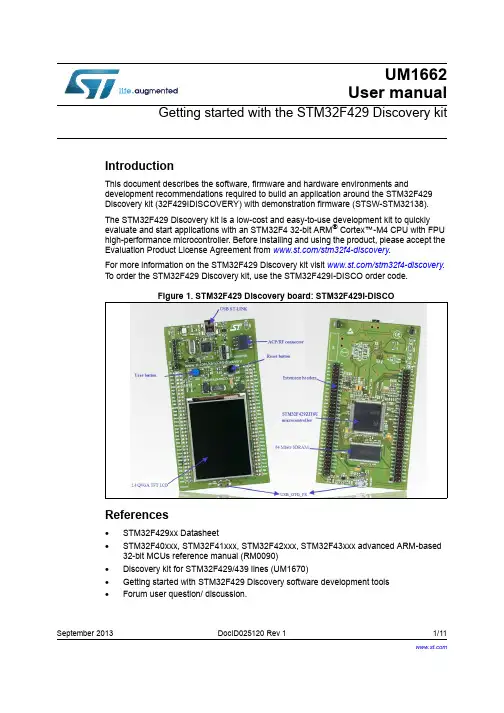
September 2013DocID025120 Rev 11/11UM1662User manualGetting started with the STM32F429 Discovery kitIntroductionThis document describes the software, firmware and hardware environments anddevelopment recommendations required to build an application around the STM32F429 Discovery kit (32F429IDISCOVERY) with demonstration firmware (STSW-STM32138).The STM32F429 Discovery kit is a low-cost and easy-to-use development kit to quickly evaluate and start applications with an STM32F4 32-bit ARM ® Cortex™-M4 CPU with FPU high-performance microcontroller. Before installing and using the product, please accept the Evaluation Product License Agreement from /stm32f4-discovery .For more information on the STM32F429 Discovery kit visit /stm32f4-discovery . To order the STM32F429 Discovery kit, use the STM32F429I-DISCO order code.Figure 1. STM32F429 Discovery board: STM32F429I-DISCOReferences•STM32F429xx Datasheet•STM32F40xxx, STM32F41xxx, STM32F42xxx, STM32F43xxx advanced ARM-based 32-bit MCUs reference manual (RM0090)•Discovery kit for STM32F429/439 lines (UM1670)•Getting started with STM32F429 Discovery software development tools •Forum user question/ discussion.Contents UM1662Contents1Hardware configuration and layout . . . . . . . . . . . . . . . . . . . . . . . . . . . . . 41.1Features . . . . . . . . . . . . . . . . . . . . . . . . . . . . . . . . . . . . . . . . . . . . . . . . . . . 41.2Microcontroller . . . . . . . . . . . . . . . . . . . . . . . . . . . . . . . . . . . . . . . . . . . . . . 41.3System requirement . . . . . . . . . . . . . . . . . . . . . . . . . . . . . . . . . . . . . . . . . . 51.4Powering up the board . . . . . . . . . . . . . . . . . . . . . . . . . . . . . . . . . . . . . . . . 51.5Reset the board . . . . . . . . . . . . . . . . . . . . . . . . . . . . . . . . . . . . . . . . . . . . . 61.6Hardware block diagram . . . . . . . . . . . . . . . . . . . . . . . . . . . . . . . . . . . . . . 62Firmware package . . . . . . . . . . . . . . . . . . . . . . . . . . . . . . . . . . . . . . . . . . . 72.1Package description . . . . . . . . . . . . . . . . . . . . . . . . . . . . . . . . . . . . . . . . . . 72.2Programming firmware application . . . . . . . . . . . . . . . . . . . . . . . . . . . . . . . 72.2.1Programming application . . . . . . . . . . . . . . . . . . . . . . . . . . . . . . . . . . . . . 82.2.2Run pre-loaded demo . . . . . . . . . . . . . . . . . . . . . . . . . . . . . . . . . . . . . . . 8 3Revision history . . . . . . . . . . . . . . . . . . . . . . . . . . . . . . . . . . . . . . . . . . . 102/11DocID025120 Rev 1UM1662List of figures List of figuresFigure 1.STM32F429 Discovery board: STM32F429I-DISCO . . . . . . . . . . . . . . . . . . . . . . . . . . . . . . 1 Figure 2.STM32F429I-DISCO power sources . . . . . . . . . . . . . . . . . . . . . . . . . . . . . . . . . . . . . . . . . . 7 Figure 3.Hardware block diagram. . . . . . . . . . . . . . . . . . . . . . . . . . . . . . . . . . . . . . . . . . . . . . . . . . . . 8 Figure 4.Package contents. . . . . . . . . . . . . . . . . . . . . . . . . . . . . . . . . . . . . . . . . . . . . . . . . . . . . . . . . 9 Figure 5.Hardware environnement. . . . . . . . . . . . . . . . . . . . . . . . . . . . . . . . . . . . . . . . . . . . . . . . . . 11DocID025120 Rev 13/111 Hardware configuration and layout1.1 FeaturesThe STM32F429 Discovery offers the following features:•STM32F429ZIT6 microcontroller featuring 2 MB of Flash memory, 256 KB of RAM in an LQFP144 package•On-board ST-LINK/V2 with selection mode switch to use the kit as a standalone ST-LINK/V2 (with SWD connector for programming and debugging)•Board power supply: through the USB bus or from an external 3 V or 5 V supply voltage•L3GD20, ST MEMS motion sensor, 3-axis digital output gyroscope•TFT LCD (Thin-film-transistor liquid-crystal display) 2.4", 262K colors RGB,240x320dots•SDRAM 64 Mbits (1Mbit x 16-bit x 4-bank) including an AUTO REFRESH MODE, anda power-saving•Six LEDs:–LD1 (red/green) for USB communication–LD2 (red) for 3.3 V power-on–Two user LEDs:LD3 (green), LD4 (red)–Two USB OTG LEDs:LD5 (green) VBUS and LD6 (red) OC (over-current)•Two pushbuttons (user and reset)•USB OTG with micro-AB connector•Extension header for LQFP144 I/Os for a quick connection to the prototyping board and an easy probing1.2 MicrocontrollerThe STM32F429ZIT6U device is based on the high-performance ARM® Cortex™-M4 32-bitRISC core operating at a frequency of up to 180 MHz The Cortex-M4 core features aFloating point unit (FPU) single precision which supports all ARM single-precisiondata-processing instructions and data types. It also implements a full set of DSP instructionsand a memory protection unit (MPU) which enhances application security.The STM32F429ZIT6U device incorporates high-speed embedded memories (2Mbytes ofFlash memory, 256 Kbytes of SRAM), up to 4 Kbytes of backup SRAM, and an extensiverange of enhanced I/Os and peripherals connected to two APB buses, two AHB buses anda 32-bit multi-AHB bus matrix.4/11DocID025120 Rev 1DocID025120 Rev 15/111.3 System requirement•Windows PC (XP , Vista, 7)•USB type A to Mini-B USB cable •ST-LINK/V2•Supported IDE are EWARM (IAR Embedded Workbench ®), MDK-ARM™ and AtollicTrueSTUDIO ®Note:Required information to download and install desired IDE and ST-LINK/V2 are detailed in Getting started with STM32F429 Discovery software development tools document.1.4 Powering up the boardThe STM32F429I-DISCO board can be powered up from three sources.•USB ST-LINK: To power the board from the USB connector CN1, use the 'USB type Ato Mini-B' cable and connect it between the host and the board USB connector CN1. •External sources: DC power supply can be inserted in the GND and 3V (or 5V) pin.Figure 2. STM32F429I-DISCO power sourcesUSB ST-LINK (CN1)5V 3V1.5 Reset the boardThere are three ways to reset the board:•Push the reset button mounted on the STM32F429I-DISCO.•Remove and reinsert the USB cable.•The MCU can also be reset by debuggers.1.6 Hardware block diagramThe STM32F429I-DISCO is designed around the STM32F429ZIT6U microcontroller in a144-pin LQFP package. Figure3 illustrates the connections between the STM32F429ZIT6Uand its peripherals (STLINK/V2, pushbutton, LED, USB and connectors).Please refer to schematic under /stm32f4-discovery for more details.6/11DocID025120 Rev 1DocID025120 Rev 17/11UM1662Firmware package2 Firmware packageTo get started with the STM32F429 Discovery kit, a firmware package that contains a set ofIP examples and demonstrations of some features exists under /stm32f4-discovery .2.1 Package descriptionThe STM32F429 Discovery firmware applications, demonstration and IPs examples areprovided in one single package and supplied in one single zip file. The extraction of the zip file generates one folder, STM32F429I-Discovery_FW_VX.Y.Z , which contains the following subfolders:Figure 4. Package contentsUser can run examples provided within this package. A set of examples for each peripheral are ready to be run.2.2 Programming firmware applicationTo start programming, user must:•Install preferred Integrated Development Environment (IDE)•Install the ST-LINK V2 driver from ST web siteFirmware package UM16628/11DocID025120 Rev 12.2.1 Programming applicationTo program application (demonstration or example), follow the sequence below:1.Go under application folder 2. Chose the desired IDE project3. Double click on the project file (ex. STM32F429I-Discovery_Demo.eww for EWARM)4. Rebuild all files: Project->Rebuild all5.Load project image: Project->Debug6. Run program: Debug->GoPlease refer to Getting started with STM32F429 Discovery software development toolsfor more details.2.2.2 Run pre-loaded demoTo run and develop any firmware applications on your STM32F429 Discovery board, theminimum requirements are as follows:–Windows PC (XP , Vista, 7)–‘USB type A to Mini-B' cable, used to power the board (through USB connector CN1) from host PC and connect to the embedded ST-LINK/V2 for debugging and Programming.Additional hardware accessories will be needed to run some applications:–‘USB type A to Micro-B' cable, used to connect the board (through USB connector CN5) as USB Device to host PC.DocID025120 Rev 19/11UM1662Firmware packageEstablish the connection with the STM32F429 Discovery board as follows:Figure 5. Hardware environnementThe demonstration software, based on the STemWin GUI library, is already preloaded in the board's Flash memory. It uses the LCD TFT mounted on the board to show the Menu based-on-icon view widget (Image Browser, Game, Performance, Clock/Calendar, Video and System Info module). The status bar indicate the CPU Usage, date, USB disk flash connection state, alarm and time.Follow the sequence below to configure the STM32F429 Discovery board and launch the DISCOVER application:1.Ensure that the jumpers JP3 and CN4 are set to "on" (Discovery mode).2.Connect the STM32F429 Discovery board to a PC using a USB cable type A/mini-B through the USB ST-LINK connector CN1, to power the board. The LEDs LD2 (PWR) and LD1 (COM).3.The following applications are available on the screen:–Clock/Calendar and Game–Video Player and Image Browser (play videos and view images from the USB mass storage connected to CN6)–Performance monitor (watch the CPU load and run a graphical benchmark)–System Info4. The demo software, as well as other software examples that allow you to discover the STM32 F4 series features, are available on /stm32f4-discovery .5.Develop your own applications starting from the examples.Revision history UM166210/11DocID025120 Rev 13 Revision historyTable 1. Document revision historyDate Revision Changes09-Sep-20131Initial release.UM1662Please Read Carefully:Information in this document is provided solely in connection with ST products. STMicroelectronics NV and its subsidiaries (“ST”) reserve the right to make changes, corrections, modifications or improvements, to this document, and the products and services described herein at any time, without notice.All ST products are sold pursuant to ST’s terms and conditions of sale.Purchasers are solely responsible for the choice, selection and use of the ST products and services described herein, and ST assumes no liability whatsoever relating to the choice, selection or use of the ST products and services described herein.No license, express or implied, by estoppel or otherwise, to any intellectual property rights is granted under this document. If any part of this document refers to any third party products or services it shall not be deemed a license grant by ST for the use of such third party products or services, or any intellectual property contained therein or considered as a warranty covering the use in any manner whatsoever of such third party products or services or any intellectual property contained therein.UNLESS OTHERWISE SET FORTH IN ST’S TERMS AND CONDITIONS OF SALE ST DISCLAIMS ANY EXPRESS OR IMPLIED WARRANTY WITH RESPECT TO THE USE AND/OR SALE OF ST PRODUCTS INCLUDING WITHOUT LIMITATION IMPLIED WARRANTIES OF MERCHANTABILITY, FITNESS FOR A PARTICULAR PURPOSE (AND THEIR EQUIVALENTS UNDER THE LAWS OF ANY JURISDICTION), OR INFRINGEMENT OF ANY PATENT, COPYRIGHT OR OTHER INTELLECTUAL PROPERTY RIGHT.ST PRODUCTS ARE NOT DESIGNED OR AUTHORIZED FOR USE IN: (A) SAFETY CRITICAL APPLICATIONS SUCH AS LIFE SUPPORTING, ACTIVE IMPLANTED DEVICES OR SYSTEMS WITH PRODUCT FUNCTIONAL SAFETY REQUIREMENTS; (B) AERONAUTIC APPLICATIONS; (C) AUTOMOTIVE APPLICATIONS OR ENVIRONMENTS, AND/OR (D) AEROSPACE APPLICATIONS OR ENVIRONMENTS. WHERE ST PRODUCTS ARE NOT DESIGNED FOR SUCH USE, THE PURCHASER SHALL USE PRODUCTS AT PURCHASER’S SOLE RISK, EVEN IF ST HAS BEEN INFORMED IN WRITING OF SUCH USAGE, UNLESS A PRODUCT IS EXPRESSLY DESIGNATED BY ST AS BEING INTENDED FOR “AUTOMOTIVE, AUTOMOTIVE SAFETY OR MEDICAL” INDUSTRY DOMAINS ACCORDING TO ST PRODUCT DESIGN SPECIFICATIONS. PRODUCTS FORMALLY ESCC, QML OR JAN QUALIFIED ARE DEEMED SUITABLE FOR USE IN AEROSPACE BY THE CORRESPONDING GOVERNMENTAL AGENCY.Resale of ST products with provisions different from the statements and/or technical features set forth in this document shall immediately void any warranty granted by ST for the ST product or service described herein and shall not create or extend in any manner whatsoever, any liability of ST.ST and the ST logo are trademarks or registered trademarks of ST in various countries.Information in this document supersedes and replaces all information previously supplied.The ST logo is a registered trademark of STMicroelectronics. All other names are the property of their respective owners.© 2013 STMicroelectronics - All rights reservedSTMicroelectronics group of companiesAustralia - Belgium - Brazil - Canada - China - Czech Republic - Finland - France - Germany - Hong Kong - India - Israel - Italy - Japan - Malaysia - Malta - Morocco - Philippines - Singapore - Spain - Sweden - Switzerland - United Kingdom - United States of AmericaDocID025120 Rev 111/11。
【STM32F429开发板用户手册】第29章STM32F429的系统bootloader之。。。
【STM32F429开发板⽤户⼿册】第29章STM32F429的系统bootloader之。
第29章 STM32F429的系统bootloader之USB DFU⽅式固件升级本章节为⼤家讲解使⽤系统bootloader做程序升级的⽅法,即使不依赖外部boot引脚也可以⽅便升级。
DFU的全称是Device Firmware Upgrade,即设备固件升级29.1 初学者重要提⽰29.2 跳转到系统bootloader的程序设计29.3 STM32CubeProg的安装说明29.3 STM32CubeProg的程序下载说明29.4 USB DFU⽅式系统bootloader驱动移植和使⽤29.6 实验例程设计框架29.7 实验例程说明(MDK)29.8 实验例程说明(IAR)29.9 总结29.1 初学者重要提⽰1. 学习本章节前,务必优先学习第28章。
2. 本章⽤到的相关软件和⽂档下载:。
3. 软件STM32CubeProg和DfuSe都⽀持USB DFU,但是两个软件不能都安装使⽤,因为这两个软件的USB驱动不同,导致⼯作在系统bootloader模式的板⼦通过USB线接到电脑端时,只有⼀个软件的驱动被识别。
4. DfuSe是⽼版的USB DFU软件,不推荐⼤家使⽤了。
建议使⽤STM32CubeProg,此软件实现了之前的DfuSe,STLINK⼩软件和Flashloader三合⼀,并且⽀持外部EEPROM,NOR Flash,SPI Flash,NAND Flash等烧写,也⽀持OTA编程。
5. 本章节的USB DFU的下载软件采⽤STM32CubeProg,如果想使⽤DfuSe的话,此贴有详细说明:。
6. 当芯⽚⼯作在系统bootLoader的USB DFU模式,更新完毕程序后,不会⾃动退出USB DFU,需要重新复位芯⽚后才会退出。
由于DFU模式会⽤到USB线,插拔USB线是难以避免的,所以是否⽀持⾃动退出,并不影响。
STM32学习笔记(一)——初入门F429
STM32学习笔记(⼀)——初⼊门F429⼀、前情电⼦信息专业,有嵌⼊式开发项⽬的经验,但不算完全了解。
上课没认真听,项⽬全靠吃⽼本,现在为了毕业设计和⼯作打算认真从头学习嵌⼊式开发。
⼆、⽬前情况看了⼀个星期正点原⼦关于STM32F429库函数开发的书,主要看的部分是ucos、fatfs和⾳乐播放器这⼏个部分,看的稀⾥糊涂的,应该是因为基础太差。
从头开始看之后,明⽩了很多,但还有很多稀⾥糊涂。
就去看了野⽕的资料,野⽕写的很好,看完清晰⾥很多,包括寄存器概念,⼿册的应⽤这种基础知识都写得很清晰明了,推荐⼤家看野⽕的教材。
我⽬前的打算是看野⽕的教材,⽤正点原⼦的例程和开发板。
正点原⼦的各种项⽬做的确实很好很有参考性。
三、笔记(⼀)STM32芯⽚图M4内核是ARM公司做的,芯⽚集成设计由ST设计的。
除内核以外的部分,是⽚上外设,内核与总线之间通过各种总线连接,其中其中主控总线有8条,被控总线有7条,具体见图其中圆圈的部分表⽰可以通信,黄⾊部分是主控总线,粉⾊部分是被控总线。
(⼆)存储器映射存储器本⾝不具有地址信息,它的地址是由芯⽚⼚商或⽤户分配,给存储器分配地址的过程就称为存储器映射,具体见图。
如果给存储器再分配⼀个地址就叫存储器重映射。
这4GB的地址空间中,ARM已经粗线条的平均分成了8个块,每块512MB,每个块也都规定了⽤途,具体分类见表格。
Boock0⽤来设计成内部FLASH,Block1⽤来设计成内部RAM,Block2⽤来设计成⽚上的外设。
这是⽐较重要的三块。
(三)寄存器映射Block2⽚上外设,四个字节为⼀单元,共32bit,每⼀单元对应不同的功能,控制这些单元时就可以控制不同外设。
除了找到每个单元的起始地址,然后通过C语⾔指针的操作⽅式来访问这些单元外,还们可以根据每个单元功能的不同,以功能为名给这个内存单元取⼀个别名,这个别名就是我们经常说的寄存器,这个给已经分配好地址的有特定功能的内存单元取别名的过程就叫寄存器映射。
STM32F429开发套件入门指南
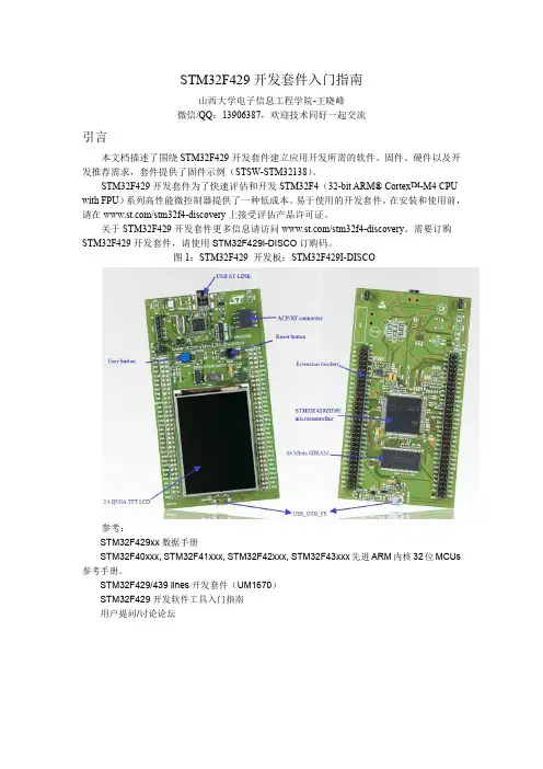
STM32F429开发套件入门指南山西大学电子信息工程学院-王晓峰微信/QQ:13906387,欢迎技术同好一起交流引言本文档描述了围绕STM32F429开发套件建立应用开发所需的软件、固件、硬件以及开发推荐需求,套件提供了固件示例(STSW-STM32138)。
STM32F429开发套件为了快速评估和开发STM32F4(32-bit ARM®Cortex™-M4CPU with FPU)系列高性能微控制器提供了一种低成本、易于使用的开发套件。
在安装和使用前,请在/stm32f4-discovery上接受评估产品许可证。
关于STM32F429开发套件更多信息请访问/stm32f4-discovery。
需要订购STM32F429开发套件,请使用STM32F429I-DISCO订购码。
图1:STM32F429开发板:STM32F429I-DISCO参考:STM32F429xx数据手册STM32F40xxx,STM32F41xxx,STM32F42xxx,STM32F43xxx先进ARM内核32位MCUs 参考手册。
STM32F429/439lines开发套件(UM1670)STM32F429开发软件工具入门指南用户提问/讨论论坛目录1硬件组成和布局1.1特性1.2微控制器1.3系统要求1.4开发板上电1.5复位开发板1.6硬件框图2固件包2.1固件包描述2.2编程固件应用2.2.1编程应用2.2.2运行预加载演示3版本历史1硬件组成和布局1.1特性STM32F429Discovery具有以下特性:STM32F429ZIT6微控制器,2MB闪存,256KBRAM,144脚LQFP封装板载ST-LINK/V2,带有选择模式接口,可作为独立的ST-LINK/V2使用(使用SWD 接口可编程和仿真)。
通过USB或外部3V,5V电源供电。
L3GD20,ST微机电动作传感器,3轴数字输出陀螺仪。
2.4寸TFTLCD,262K色RGB,分辨率240*320。
stm32f429数据手册
stm32f429数据手册一、导言对于嵌入式开发者来说,芯片的数据手册是一本非常重要的工具书。
其中,STM32F429数据手册堪称StMicroelectronics公司旗下MCU产品系列中的精华之作。
本文将深入探讨STM32F429数据手册,介绍其内容以及如何使用。
二、概述STM32F429是一款高性能、低功耗的32位ARM Cortex-M4微控制器。
数据手册提供了有关芯片的各种技术规格、功能介绍、外设接口等信息。
通过阅读数据手册,开发者可以深入了解芯片的架构和特性,为开发过程提供全面准确的参考。
三、产品特点1.性能卓越STM32F429运行频率高达180MHz,拥有强大的运算能力。
通过浏览数据手册,我们可以了解到芯片的内核、存储器以及时钟配置等方面的详细信息。
2.丰富的外设芯片支持多种通信接口,如UART、SPI、I2C等。
此外,它还拥有USB、SDIO、CAN等高级外设接口,方便连接外部设备。
3.多样的功耗模式数据手册中提供了关于芯片不同功耗模式的详细说明。
通过配置相应的寄存器,我们可以将芯片在不同场景下的功耗控制在合理范围内,从而节约能源并延长电池寿命。
四、引脚布局数据手册中包含了芯片的引脚图及其功能说明。
开发者可以通过阅读数据手册了解每个引脚的功能,并根据需要进行连接。
五、模块详解1.系统和存储器模块在这个模块中,我们可以了解到关于芯片的系统时钟、复位源、存储器类型、位带模式等方面的详细信息。
通过合理配置这些参数,我们可以优化系统性能和资源利用。
2.中断和异常模块芯片中的中断控制器可以管理多个中断源,并按照优先级对中断进行处理。
数据手册中提供了中断优先级分组规则、清除中断标志位的方法等详细说明,有助于开发者合理处理中断。
3.通信接口模块该模块详细介绍了芯片支持的各种通信接口的工作原理和使用方法。
例如,数据手册中对SPI接口的时序图、I2C接口的总线速率计算公式等进行了清晰的解释,为开发者提供了技术支持。
STM32F429I-DISCO开发板用户手册说明书
Open429Z-D User ManualContents1. Hardware introduction (2)1.1. What’s on board (2)2. Demo (4)2.1. ADC+DMA (4)2.2. CAN1 TO CAN2-Normal (5)2.3. DAC (5)2.4. DS18B20 (6)2.5. OV2640 (6)2.6. GPIO_Key (7)2.7. I2C (7)2.8. I2S_UDA1380 (8)2.9. NandFlash_SCB0 (8)2.10. SAI (9)2.11. SD_FatFS (9)2.12. SDIO (9)2.13. SPI (10)2.14. USART (11)3. Version update records (11)1. Hardware introduction 1.1. What’s on board[ Core interface ]1. STM32F429I-DISCO socketfor easily connecting the STM32F429I-DISCO 2. MCU pins connectorall the MCU I/O ports are accessible onexpansion connectors for further expansion 3. USB connectorUSB to UART via PL2303 USB TO UART board onboard MCU4. I2C1 / I2C2interface[ Other interfaces ]16. 5V DC jack17. 5V/3.3 V power input/outputusually used as power output, alsocommon-grounding with other user board 18. JTAG/SWD interfacefor debugging/programming[ Jumper ]easily connects to I2C peripherals such as I/O expander (PCF8574), FRAM (FM24CLXX), etc. 5. I2S2 / I2S3 / I2C1 interfacefor connecting I2S peripherals, such as Audio module.6. DCMI interfacefor connecting camera module 7. SDIO interfacefor connecting Micro SD module, features much faster access speed rather than SPI 8. CAN1 interfacecommunicates with accessory boards which feature the CAN device conveniently 9. CAN2 interfacecommunicates with accessory boards which feature the CAN device conveniently 10. UART3 interfaceeasily connects to RS232, RS485, USB TO 232, etc11. SPI1/SPI4 + AD/DA interfaceeasily connects to SPI peripherals such as DataFlash (AT45DBxx), SD card, MP3 module, etc MP3SPI1 features AD/DA alternative function, supports connecting AD/DA module as well 12. UART2 interfaceeasily connects to RS232, RS485, USB TO 232, etc13. 8-bit FSMC interfaceeasily connects to peripherals such as NandFlash, Ethernet, etc 14. SAI1 interfacefor connecting Audio peripherals, such as UDA1380 etc15. One-WIRE interfaceeasily connects to ONE-WIRE devices (TO-92 package), such as temperature sensor (DS18B20), electronic registration number (DS2401), etc.16. Joystick jumpershort the jumper to connect the joystick to default I/Os used in example code;open the jumper to connect the joystick to custom I/Os via jumper wires. 17. BOOT mode switchfor configuring BOOT0 pin 18. USB TO UART jumper[ Components ] 16. AMS1117-3.33.3V voltage regulator 17. PL2303USB to UART MCU 18. 5V DC jack 19. Power LED20. UART1 indicator LED 21. Joystickfive positions2. DemoKEIL MDK Version :4.7Programmer/Debugger: STM32F429I-DISCO onboard ST-LINK V2 Programming/Debugging interface: SWDConnect PC to the onboard USB TO UART connector via USB wireSerial port settings:2.1. ADC+DMA◆ OverviewAD acquisition demo◆ Hardware connectionConnect Analog Test Boardto SPI1(ADC+DAC )connector◆ Operation and resultRotate the onboard potentiometer, the below message will be printed on the serial debugging assistant:Select a proper COM port Baud rate115200Data bits 8Stop bits 1 Parity bits None Flow controlNone2.2. CAN1 TO CAN2-Normal◆ OverviewCAN demo◆ Hardware connection◆ Hardware connectionConnect the two CAN modules to theonboard CAN interfaces◆ Operation and resultYou may see the below result on the serial debugging assistant:2.3. DAC◆ OverviewDAC demo◆ Hardware connectionConnect the Analog Test Board to the SPI1(ADC+DAC )connectorConnect the Analog Test Board onboard 5Vinterface to the board onboard 5V interface viajumper wire.◆ Operation and resultYou may hear sound from the Analog Test Board2.4. DS18B20◆ OverviewDS18B20 demo◆ Hardware connectionConnect the DS18B20 module to the one-wire connector ◆ Operation and resultThe below information will be printed on the serial debugging assistant2.5. OV2640◆ OverviewCamera OV2640 demo ◆ Hardware connectionConnect the OV2640 Camera Board tothe onboard DCMMI connectorLaunch the serial debugging assistant, configuring the data as below: COM: COM3Baud rate: 115200 Data bits: 8 Parity bits: NO Stop bits: 1◆ Operation and result:Press “user” key, the captured image displayed on the serial debugging assistant:2.6. GPIO_Key◆ Overviewjoystick demo◆ Hardware connectionShort the JOYSTICK JMP on board ◆ Operation and resultPress the joystick, message will be printed on the serial debugging assistant accordingly.2.7. I2C◆ OverviewI2C EEPROM demo ◆ Hardware connectionConnect the AT24/FM24 Board to the board viaI2C connector (I2C1 or I2C2, depending on the software configuration).◆ Software configurationThe module connect to I2C1 connectorThe module connect to I2C2 connector #define Open_I2C1 //#define Open_I2C2//#define Open_I2C1 #define Open_I2C2◆ Operation and resultThe below information will be printed on the serial debugging assistant:2.8. I2S_UDA1380◆ OverviewI2S_UDA1380 demo ◆ Hardware connectionConnect the UDA1380 Board to the board via I2Sconnector.Connect the earphone to the UDA1380 Board viaLINEOUT connector◆ Operation and resultYou should hear music when press the RESET key2.9. NandFlash_SCB0◆ OverviewNandFlash demo ◆ Hardware connectionConnect the NandFlash Board to theboard via I2C2 connector.◆ Operation and resultThe below information will be printed on the serial debugging assistant:2.10. SAI◆ OverviewSAI demo◆ Hardware connectionConnect UDA1380 Board to the board via SAI1connector.Connect the earphone to the UDA1380 Board viaLINEOUT connector.◆ Operation and resultYou should hear music when press the RESET key.2.11. SD_FatFS◆ OverviewSD_FatFS demo ◆ Hardware connectionConnect the Micro SD Storage Board to theboard via SDIO connector.Insert the SD card to the Micro SD Storage Board socket.◆ Operation and resultMessage will be printed on the serial debugging assistant.2.12. SDIO◆ OverviewSDIO demo◆Hardware connectionConnect the Micro SD Storage Board to theboard via SDIO connector.Insert the SD card to the Micro SD Storage Board socket.◆ Operation and resultMessage will be printed on the serial debugging assistant.2.13. SPI◆ OverviewSPI demo◆ Hardware connectionConnect the AT45DBXX DataFlash Board via SPIconnector. (SPI1 or SPI4, depending on the software configuration◆ Software connectionModule connect to SPI1 connectorModule connect toSPI4 connector #define Open_SPI1 //#define Open_SPI4//#define Open_SPI1 #define Open_SPI4◆ Operation and resultInfo/messages printed on the serial debugging assistant:11 2.14. USART◆ OverviewUSART demo◆ Hardware connection◆ Operation and resultInfo/messages printed on the serial debugging assistant:3. Version update records VersionModification Date Author V1.0Initial Release 2014/05/17 Waveshare team。
Open429I -C 用户手册说明书
1.Open429I-C is an STM32 development board designed for the STM32F429IGT6 microcontroller, consists of the mother board and the MCU core board Core429I.The Open429I-C supports further expansion with various optional accessory boards for specific application. The modular and open design makes it the ideal for starting applicationdevelopment with STM32 series microcontrollers.1.1.WHAT'S ON THE MOTHER BOARD1.MCU core board connector: for easilyconnecting the Core429IART3 interface: easily connects to RS232,RS485, USB TO 232, etc.3.DCMI interface: for connecting camera4.Capacitive touch panel interface: forconnecting capacitive touch panel5.CAN2 interface: for connecting CANmodules6.CAN1 interface: for connecting CANmodules7.SDIO interface: for connecting Micro SDmodule, features much faster access speedrather than SPI8.ULPI interface: for connecting high-speedUSB peripheral (the STM32F429I integratesUSB HS controller without any PHY device)9.LCD interface 1: for connecting 7inch LCD10.ONE-WIRE interface: easily connects toONE-WIRE devices (TO-92 package), such astemperature sensor (DS18B20), electronicregistration number (DS2401), etc.11.LCD interface 2: for connecting 4.3inch LCD12.I2C2/I2C3 interface: easily connects to I2Cperipherals such as I/O expander (PCF8574),EEPROM (AT24Cxx), etc.13.SAI1 interface: for connecting audiomodules like UDA1380 module14.Ethernet interface: for connecting EthernetmodulesB connector: USB to UART via theonboard convertor PL230316.SPI1/SPI2 interfaces:●easily connects to SPI peripherals suchas DataFlash (AT45DBxx), SD card, MP3module, etc.●easily connects to AD/DA modules(SPI1 features AD/DA alternativefunction) 17.I2S2/I2S3/I2C1 interface: easily connects toI2S peripherals such as audio module, etc.18.8-bit FMC interface: easily connects toperipherals such as NandFlash19.5V DC jack20.5V/3.3V power input/output: usually usedas power output, also common-groundingwith other user board21.MCU pins connector: all the MCU I/O portsare accessible on expansion connectors forfurther expansion22.PL2303: USB to UART convertor23.LEDs: convenient for indicating I/O statusand/or program running state24.PL2303 TX-LED / RX-LED25.12MHz crystal: for PL230326.Joystick: five positions27.WAKE UP button: used as regular button,and/or wake up the STM32 MCU from sleepB to UART jumper29.LED jumper●short the jumper to connect to defaultI/Os used in example code●open the jumper to connect to customI/Os via jumper wires30.Button/Joystick jumper●short the jumper to connect to defaultI/Os used in example code●open the jumper to connect to customI/Os via jumper wires1.2.WHAT'S ON THE CORE429I1.STM32F429IGT6: the high performance STM32 MCU which features:●Core: Cortex-M4 32-bit RISC●Feature: single-cycle DSP instructions●Operating Frequency: 180MHz, 225 DMIPS/1.25 DMIPS/MHz●Operating Voltage: 1.8V-3.6V●Package: LQFP176●Memories: 1024kB Flash, 256+4kB SRAM●MCU communication Interfaces:● 6 x SPI, 4 x USART, 4 x UART, 2 x I2S, 1 x SAI, 3 x I2C● 1 x FMC, 1 x SDIO, 2 x CAN● 1 x LCD-TFT● 1 x USB 2.0 HS/FS controller (with dedicated DMA)● 1 x USB HS ULPI (external PHY required)● 1 x 10/100 Ethernet MAC● 1 x 8 to 14-bit camera interface●AD & DA converters: 3 x AD (12-bit, 1μs, shares 24 channels); 2 x DA (12-bit)●Debugging/Programming: supports JTAG/SWD interfaces, supports IAP2.IS42S16400J: SDRAM 1 Meg Bits x 16 Bits x 4 Banks (64-MBIT)3.AMS1117-3.3: 3.3V voltage regulator4.MIC2075: onboard USB power management device5.Power supply switch, powered from 5Vin or USB connection6.Boot mode selection, for configuring BOOT0 pin7.Power indicator8.VBUS LED9.Reset button10.8M crystal11.32.768K crystal, for internal RTC with calibration12.JTAG/SWD interface: for debugging/programmingB connector, supports Device and/or Host14.MCU pins expander, VCC, GND and all the I/O pins are accessible on expansion connectors forfurther expansion15.5Vin pinheader, 5V power supply is required when using USB HOST/OTGB OTG/HOST jumper●short the jumper when using USB OTG/HOST●open the jumper to disconnect from related I/O port17.VBAT selection jumper●short the jumper to use system power supply●open the jumper to connect the VBAT to external power, such as battery18.VREF selection jumper●short the jumper to connect VREF+ to VCC●open the jumper to connect VREF+ to other custom pin via jumper wire2.●KEIL MDK Version:4.7 or above.●Programmer/Debugger: STM32F429I-DISCOonboard ST-LINK V2●Programming/Debugging interface:JTAG/SWD●Results of demo which based on serial port are all checked via onboard PL2303; connect the USBcable to the USB TO UART interface.●PC’s serial port settings:Baud rate 115200Data bits 8Stop bits 1Parity bits NoneFlow control NoneNote: All the below Demo results are available when push the reset button after the program has been downloaded.2.1.ADC+DMA●OverviewAD acquisition demo, DMA transfer●Hardware connectionConnect Analog Test Board to SPI1 (ADC+DAC)connector●Operation and resultRotate the onboard potentiometer, the below message will be printed on the serial debugging assistant:***************************************The current AD1 value = 2.98VThe current AD2 value = 1.87V***************************************The current AD1 value = 2.86VThe current AD2 value = 1.75V2.2.CAN1 TO CAN2-NORMAL●OverviewCAN1 TO CAN2 communication demo●Hardware connectionConnect the two CAN modules to the onboard CAN1 and CAN2 interfaceConnect the two CAN modules via jumper wire (CANL<->CANL, CANH<->CANH) ●Operation and resultYou may see the below result on the serial debugging assistant:SYSCLK: 168MHCLK: 168MPCLK1: 42MPCLK2: 84MCAN Printf Example: Press the USER key observationsCAN2 Receive DataCAN2 ID 123CAN2_DATA0 34CAN2_DATA1 a2CAN2_DATA2 d8CAN2_DATA3 42CAN2_DATA4 a1CAN2_DATA5 44CAN2_DATA6 a4CAN2_DATA7 69CAN1 Receive DataCan1 ID 3212.3.DAC●OverviewDA output demo, output via DMA channel●Hardware connectionConnect the Analog Test Board to the SPI1 (ADC+DAC)connectorConnect the Analog Test Board onboard 5V interface to the board onboard 5V interface via jumper wire.●Operation and resultYou may hear sound from the Analog Test Board.2.4.DS18B20●OverviewDetect the temperature by DS18B20.●Hardware connectionConnect the DS18B20 to the one-wire socket●Operation and resultThe below information will be printed on the serial debugging assistantSYSCLK: 168MHCLK: 168MPCLK1: 42MPCLK2: 84MDS18B20 ExampleDS18B20’s ID: 0x28 0x76 0xfe 0x49 0x5 0x0 0x0 0x76Temperature: 0.8℃Temperature: 85.0℃Temperature: 28.0℃Temperature: 27.93℃2.5.GPIO_LED_KEY●OverviewIO input, output demo●Hardware connectionFit all the jumpers LED JMP (PF6, PF7, PF8, PF9), JOYSTICK JMP.●Operation and resultThe LED status will keep changing when push the buttons.2.6.I2C●OverviewRead and write data on E2PROM via I2C protocol●Hardware connectionConnect the AT24/FM24 Board to the board via I2C connector (I2C1 or I2C2, depending on the software configuration).●Software configurationConnect the module to I2C1 interface Connect the module to I2C2 interface#define Open_I2C1 //#define Open_I2C2 //#define Open_I2C1 #define Open_I2C2●Operation and resultThe below information will be printed on the serial debugging assistant: *********I2C Example*****************SYSCLK: 180MHCLK: 180MPCLK1: 45MPCLK2: 90MEEPROM 24C02 Write TestEEPROM 24C02 Write Test OKEEPROM 24C02 Write TestEEPROM 24C02 Write Test OK2.7.I2S_UDA1380●OverviewDrive the UDA1380 Board to play music via I2S protocol●Hardware connectionConnect the UDA1380 Board to the board via I2S interface.Connect the earphone to the UDA1380 Board via LINEOUT interface●Operation and resultYou should hear music when press the RESET key.The below information will be printed on the serial debugging assistant: SYSCLK: 180MHCLK: 180MPCLK1: 45MPCLK2: 90MWelcome to use UDA1380 I2S test:WaveDataLength: 1003324Started to Transmission data.UDA1380 Init OK!AudioRemSize: 370563AudioRemSize: 305028AudioRemSize: 239493AudioRemSize: 173958AudioRemSize: 108423AudioRemSize: 42888AudioRemSize: 0AudioRemSize: 0Data transmission to completeStarted to Transmission data2.8.LCD_4.3INCH●OverviewThe 4.3inch LCD resolution is 272 x480 (Pixel); with stand-alone touch controller.LCD display character demo.●Hardware connectionConnect the 4.3inch 480x272 Touch LCD (B) to the board via LCD interface.●Operation and resultInformation display on the LCD:2.9.LCD_7INCH●OverviewThe 7inch Resistive Touch LCD resolution is 800x480 (Pixel).The 7inch Capacitive Touch LCD is also compatible with this board, the display result is the same.LCD display character demo.●Hardware connectionConnect the 7inch Capacitive Touch LCD to the LCD interface 1 using 40PIN FFC wire, and to the Capacitive touch panel interface via 4PIN FFC.Connect the 7inch Resistive Touch LCD to the board via LCD interface 1 using 40PIN FFC wire.For more details of interfaces, please read 1.1 What's on the mother board.●Operation and resultInformation display on the LCD2.10.NANDFLASH_SCB0●OverviewRead and write NAND FLASH via FSMC●Hardware connectionConnect the NandFlash Board to the board via 8BIT FSMC interface.●Operation and resultThe below information will be printed on the serial debugging assistant:SYSCLK: 180MHCLK: 180MPCLK1: 45MPCLK2: 90MWelcome to use NAND FLASH modules*********************************************************Nand Flash ID = EC, F1, 00, 95 Type = K9F1G08U0BWritten to the number of:1 2 3 4 5 6 7 8 9 a b c d e f 10 11 122.11.OV2640●OverviewThe development board communicates with the PC via Ethernet●Hardware connectionConnect the OV2640 Camera Board to the onboard DCMI interface Unzip OV2640-Test-Tool.7z and run the software.●Operation and resultPress WAKE UP button, the software captured below picture:2.12.SAI●OverviewDrive the UDA1380 Board to play music via SAI interface●Hardware connectionConnect UDA1380 Board to the board via SAI1 interface.Connect the earphone to the UDA1380 Board via LINEOUT connector.●Operation and resultYou should hear music when press the RESET key.2.13.SD_FATFS●OverviewRead and write SD card, SD card is FAT file system.●Hardware connectionConnect the Micro SD Storage Board to the board via SDIO interface.Insert the SD card to the Micro SD Storage Board socket.●Operation and resultMessage will be printed on the serial debugging assistant.SYSCLK: 180MHCLK: 180MPCLK1: 45MPCLK2: 90MSDIO Example: retarget the C library printf function to the SDIO 磁盘初始化: 0 挂载磁盘: 0短文件名: BOOTCODE.BIN长文件名: bootcode.bin文件头255字节内容:短文件名: CMDLINE.TXT长文件名: cmdline.txt文件头255字节内容: dwc_otg.lpm_enable=0 console=ttyAMA0, 115200 kgdboc=ttyAMA0, 115200 console=tty1 root=/dev/mmcblk0p2 rootfstype=ext4 elevator=deadline rootwait fbcon=map:1 fbcon=foot: ProFont6x11短文件名: CONFIG.TXT长文件名: config.txt文件头255字节内容: # uncomment if you get no picture on HDMI for a default “safe”2.14.SDIO●OverviewRead and write SD card.●Hardware connectionConnect the Micro SD Storage Board to the board via SDIO interface.Insert the SD card to the Micro SD Storage Board socket.●Operation and resultMessage will be printed on the serial COM port.USART Printf Example: retarget the C library printf function to the USARTSYSCLK: 180MHCLK: 180MPCLK1: 45MPCLK2: 90MWarning: this program may erase all the TF card data. Make sure you have backed up. Press “y”to continue.警告:接下来的操作能破坏您在SD卡上的数据,请备份好SD卡内容后,在按”Y”继续操作!01. ----- SD_Init Status:42Initialize SD card successfully!02. ----- SD_GetCardInfo Status:422.15.SPI●OverviewDrive the AT45DBXX DataFlash Board via SPI interface●Hardware connectionConnect the AT45DBXX DataFlash Board via SPI connector. (SPI1 or SPI4, depends on thesoftware configuration●Software connectionConnect the module to SPI1 interface Connect the module toSPI4 interface#define Open_SPI1 //#define Open_SPI4 //#define Open_SPI1 #define Open_SPI4●Operation and resultInfo/messages printed on the serial debugging assistant:SYSCLK: 180MHCLK: 180MPCLK1: 45MPCLK2: 90MWelcome to WaveShare STM32F4 series MCU Board Open429Z-DSPI is ready!AT45DBXX had been Init!AT45DBXX ID is 0x1f 0x24 0x0 0x0FALSH AT45DBXX Write Test:0 1 2 3 4 5 6 7 8 9 10 11 122.16.STEMWIN_RTOS●OverviewSTemwin interface display based on system RTOS.●Hardware connectionConnect the 4.3inch 480x272 Touch LCD (B) to the board via LCD interface 2.●Operation and resultThe GUI interface displayed on the LCD.2.17.TOUCH_RES_LCD4.3●OverviewTouch the screen first, click the three times the calibration point [+] to finish the screencalibration.Then you can draw any line on the screen.●Hardware connectionConnect the 4.3inch 480x272 Touch LCD (B) to the board via LCD interface 2.For more details of interfaces, please read 1.1 What's on the mother board.●Operation and resultYou can draw any line on the screen.2.18.TOUCH_RES_LCD7●OverviewTap the Adjust area to start calibration, and then tap the calibration dot [+] five times to finish the screen calibration.Then you can draw any line on the screen.●Hardware connectionConnect the 7inch Resistive Touch LCD to the board via the LCD interface 1 using 40PIN FFC wire.For more details of interfaces, please read 1.1 What's on the mother board.Operation and resultInformation displayed on the LCD screen.2.19.TOUCH_CAP_LCD7●OverviewThe LCD will display touch position of your finger. The maximum touch point of this capacitive screen is 5.●Hardware connectionConnect the 7inch Capacitive Touch LCD to the on board LCD interface 1 via 40PIN FFC cable.Connect the on board CAP_TOUCH interface and the LCD 4PIN interface via 4PIN FFC cable.●Operation and resultInformation displayed on the LCD screen. (Below is five point touch result)2.20.UCOS II 2.9●OverviewLED demo based on uCos II●Operation and resultPlug in the jumper on LED and JOYSTICK. Press the key to change the LED status, the below information will be printed on the serial debugging assistant.SYSCLK: 180MHCLK: 180MPCLK1: 45MPCLK2: 90MKEY CenterKEY DKEY BKEY AKEY CKEY CenterART●OverviewUSART port communication demo●Operation and resultConnect the USB TO UART port to PC with USB-mini cable. The port is connected to USART1 by default but it can be changed by setting jumper UART1 JMP. Message will be printed on the COM port.USART Rrintf Example: retarget the C library printf function to the USARTSYSCLK: 180MHCLK: 180MPCLK1: 45MPCLK2: 90MB FS●USB FS request to short the OTG JMP and open the UART1 jumper.Display with 4.3 inch LCD Display with 7 inch LCDConnect 4.3inch 480x272 Touch LCD (B) to the board via LCD interface 2.Modify stm32f429i_discovery_lcd.h:#define inch_4//#define inch_7 Connect the 7inch Capacitive Touch LCD to the on board LCD interface 1 via 40PIN FFC cable. Connect the on board CAP_TOUCH interface and the LCD 4PIN interface via 4PIN FFC cable.ORConnect the 7inch Resistive Touch LCD to the board via the LCD interface 1 using 40PIN FFC wire.Modify stm32f429i_discovery_lcd.h://#define inch _4#define inch_7B FS EXAMPLES (USB_DEVICE_EXAMPLES-HID)●OverviewFS USB device HID demo. USB device (mouse) will appear on the PC.●Hardware connectionConnect an USB wire to the PC via Mini USB interface.Connect the LCD to the board via LCD interface.●Operation and resultUSB device appear on the PC, press the joystick to control the movement of the cursor.B FS EXAMPLES (USB_DEVICE_EXAMPLES-MSC)●OverviewFS USB device MSC demo. “USB Mass storage device” will appear on the computer Device Manager.●Hardware connectionConnect the Micro SD Storage Board to the board via SDIO interface.Insert the SD card to the Micro SD Storage Board socket.Connect an USB wire to the PC via Mini USB interface.Connect the LCD to the board via LCD interface.●Operation and result“USB Mass storage device” will appear on the computer Device Manager, the SD card appears asa removable hard drive on the PC.2.22.B FS EXAMPLES (USB_DEVICE_EXAMPLES-VCP)●OverviewFS USB device VCP demo. “STMicroelectronics Virtual COM Port” will appear on the computer Device Manager.●Hardware connectionConnect an USB wire to the PC via Mini USB interface.Connect the LCD to the board via LCD interface.●Operation and result“STMicroelectronics Virtual COM Port” will appear on the computer Device Manager.B FS EXAMPLES (USB_HOST_DEVICE_EXAMPLES-DRD)●OverviewFS USB host and device demo. You can toggle the board between host and device.●Hardware connectionConnect the LCD to the board via LCD interface.Operation and resultChoose host or device via joystick:Host:Connect an USB flash driver (with BMP picture inside) to the board through an USB OTG cable.Device:Connect the Micro SD Storage Board to the board via SDIO interface.Insert the SD card to the Micro SD Storage Board socket.Connect an USB wire to the PC via Mini USB interface.“USB Mass storage device” will appeared on the computer Device Manager, the SD card appears as a removable hard drive on the PC.B FS EXAMPLES (USB_HOST_EXAMPLES-HID)●OverviewFS USB host HID demo, the board will recognize and use mouse.●Hardware connectionConnect a USB mouse to the on board USB interface through an USB OTG cableConnect the LCD to the board via LCD interface.●Operation and resultThe green dot on the LCD will move following the mouse.B FS EXAMPLES (USB_HOST_EXAMPLES-MSC)●OverviewFS USB host MSC demo , the board will recognize and use USB memory device.●Hardware connectionConnect an USB flash driver (with BMP picture inside) to the board through an USB OTG cable.Connect the LCD to the board via LCD interface.●Operation and resultThe document name will be listed on the LCD, bmp picture will display on the LCD.2.2B HS2.2B HS EXAMPLES (USB_DEVICE_EXAMPLES-HID)●OverviewHS USB device HID demo. USB device (mouse) will appear on the PC.●Hardware connectionInsert the USB3300 to the ULPI socketConnect the USB3300 to the PC via USB cable.●Operation and resultControl the PC cursor via joystick.2.2B HS EXAMPLES (USB_DEVICE_EXAMPLES-MSC)●OverviewHS USB device MSC demo. “STMicroelectronics Virtual COM Port” will appear on the computer Device Manager.●Hardware connectionInsert the USB3300 to the ULPI socketConnect the Micro SD Storage Board to the board via SDIO interface.Insert the SD card to the Micro SD Storage Board socket.Connect the USB3300 to the PC via USB cable.●Operation and result●“USB Mass storage device” will appeare on the computer Device Manager, the SD card appearsas a removable hard drive on the PC.“STMicroelectronics Virtual COM Port” will appear on the computer Device Manager. Short the TX and RX of the UART3 on the board, launch the serial debugging assistant, the software can receive the data sent by itself.2.2B HS EXAMPLES (USB_HOST_EXAMPLES-MSC)●OverviewHS USB host MSC demo. The board will recognize and use USB memory device.●Hardware connectionInsert the USB3300 to the ULPI socketConnect the USB flash driver to the USB3300 via USB interface.●Operation and resultThe USB flash driver information will appear on the serial debugging assistant, the documents name will be displayed when press the User key.2.24.ETH EXAMPLES●OverviewThe board and the PC connect via the Ethernet interface demo.ETH demo requests to copy the echotool.exe under ETH\Tool\PC_Software to the C disk root directory.●Hardware connectionThe Ethernet wire connects to the ETH interface and the PC.●PC IP settingConfigure the IP of both the PC and the module on the same network.Use the below IP address:Operation and resultProgram path:ETH\STM32F4x7_ETH_LwIP_V1.0.0\Project\Standalone\httpserver\MDK-ARM Open the browser, enter http://192.168.1.10/Click LED control to control the LED.。
秉火STM32F429开机测试程序用户手册
类型为“TCP Server”,把软件上的“本地 IP 地址”设置为开发板上显示的服务 器 IP 地址,本例为 192.168.1.102。设置“本地端口号”为开发板上显示的端口 号,本例里为 6000,然后点击“开始监听”按钮,见图 1-16 图 1-16。
第 13 页 共 28 页
秉火 F429 至尊版用户手册
图 1-19 中文输入 (4) 部分标点输入。系统输入法提供英文标点符号,分别有:
“_”:下划线; “.”:点; “ ”:空格; “,”:逗号; “En”:回车键; “Back”:退格键。
9. Camera
点击主界面
图标可进入摄像头应用界面。Camera App 实现 OV2640 摄像头
退出输入法检测界面。
(2) 英文输入。在默认启动状态下是激活英文小写状态,直接触摸点击字母即可输入小
写字母;触摸点击右下角
按钮可切换至大写字母输入状态,同时键盘
以大写字母表示。再次触摸点击该按钮即可切换至小写字母输入状态。输入完成 退出方法同数字输入。
(3) 中文输入。在英文小写状态下触摸点击右下角
1. RGBLED
点击主界面
图标可打开 RGB 彩灯应用界面。REGLED APP 可对板子上的
RGB 彩灯进行调色,见图 1-3。APP 界面上的三个参数分别代表 RGB888 颜色格式的 R、
G、B 值,通过滑动条可设置参数值,界面下方的圆会以这三个参数合成的颜色显示,板
子上的 RGB 彩灯也会随之变换颜色。
若遇到问题无法解决,请联系我们。
STM32F429IGT6数据手册_引脚图_参数
STM32F429xx ARM Cortex-M432b MCU+FPU,225DMIPS,up to2MB Flash/256+4KB RAM,USBOTG HS/FS,Ethernet,17TIMs,3ADCs,20comm.interfaces,camera&LCD-TFTData brief Features•Core:ARM32-bit Cortex™-M4CPU with FPU,Adaptive real-time accelerator(ARTAccelerator™)allowing0-wait state executionfrom Flash memory,frequency up to180MHz, MPU,225DMIPS/1.25DMIPS/MHz(Dhrystone2.1),and DSP instructions •Memories–Up to2MB of Flash memory organized into two banks allowing read-while-write –Up to256+4KB of SRAM including64-KB of CCM(core coupled memory)data RAM –Flexible external memory controller with up to32-bit data bus:SRAM,PSRAM,SDRAM,Compact Flash/NOR/NAND memories •LCD parallel interface,8080/6800modes •LCD-TFT controller up to VGA resolution with dedicated Chrom-ART Accelerator™forenhanced graphic content creation(DMA2D)•Clock,reset and supply management– 1.8V to3.6V application supply and I/Os–POR,PDR,PVD and BOR–4-to-26MHz crystal oscillator–Internal16MHz factory-trimmed RC(1% accuracy)–32kHz oscillator for RTC with calibration–Internal32kHz RC with calibration•Low power–Sleep,Stop and Standby modes–V BAT supply for RTC,20×32bit backup registers+optional4KB backup SRAM •3×12-bit,2.4MSPS ADC:up to24channels and7.2MSPS in triple interleaved mode•2×12-bit D/A converters•General-purpose DMA:16-stream DMA controller with FIFOs and burst supportLQFP100(14×14mm)LQFP144(20×20mm)UFBGA176(10×10mm)LQFP176(24×24mm)TFBGA216(13x13mm)WLCSP143 LQFP208(28x28mm)–Cortex-M4Embedded Trace Macrocell™•Up to168I/O ports with interrupt capability –Up to164fast I/Os up to84MHz–Up to1665V-tolerant I/Os•Up to21communication interfaces–Up to3×I2C interfaces(SMBus/PMBus)–Up to4USARTs/4UARTs(11.25Mbit/s, ISO7816interface,LIN,IrDA,modemcontrol)–Up to6SPIs(42Mbits/s),2with muxed full-duplex I2S for audio class accuracy viainternal audio PLL or external clock –1x SAI(serial audio interface)–2×CAN(2.0B Active)and SDIO interface •Advanced connectivity–USB2.0full-speed device/host/OTGcontroller with on-chip PHY–USB2.0high-speed/full-speeddevice/host/OTG controller with dedicatedDMA,on-chip full-speed PHY and ULPI –10/100Ethernet MAC with dedicated DMA: supports IEEE1588v2hardware,MII/RMII •8-to14-bit parallel camera interface up to 54MBs/s•True random number generator•CRC calculation unit•96-bit unique ID•RTC:subsecond accuracy,hardware calendarTable1.Device summaryReference Part number•Up to17timers:up to twelve16-bit and two32-bit timers up to180MHz,each with up to4IC/OC/PWM or pulse counter and quadrature STM32F429xxSTM32F429VG,STM32F429ZG,STM32F429IG,STM32F429VI,STM32F429ZI,STM32F429II,STM32F429BG,STM32F429BI,STM32F429NI,STM32F429NG(incremental)encoder input•Debug mode–SWD&JTAG interfacesMay2013Doc ID023140Rev21/102 For further information contact your local STMicroelectronics sales office.Contents STM32F429xx Contents1Introduction (7)2Description (8)2.1Full compatibility throughout the family (11)3Functional overview (14)3.1ARM®Cortex™-M4with FPU and embedded Flash and SRAM (14)3.2Adaptive real-time memory accelerator(ART Accelerator™) (14)3.3Memory protection unit (14)3.4Embedded Flash memory (15)3.5CRC(cyclic redundancy check)calculation unit (15)3.6Embedded SRAM (15)3.7Multi-AHB bus matrix (15)3.8DMA controller(DMA) (16)3.9Flexible memory controller(FMC) (17)3.10LCD-TFT controller (17)3.11Chrom-ART Accelerator™(DMA2D) (18)3.12Nested vectored interrupt controller(NVIC) (18)3.13External interrupt/event controller(EXTI) (18)3.14Clocks and startup (18)3.15Boot modes (19)3.16Power supply schemes (19)3.17Power supply supervisor (19)3.17.1Internal reset ON (19)3.17.2Internal reset OFF (20)3.18Voltage regulator (21)3.18.1Regulator ON (21)3.18.2Regulator OFF (22)3.18.3Regulator ON/OFF and internal reset ON/OFF availability (25)3.19Real-time clock(RTC),backup SRAM and backup registers (25)3.20Low-power modes (26)3.21V BAT operation (27)2/102Doc ID023140Rev2STM32F429xx Contents3.22Timers and watchdogs (27)3.22.1Advanced-control timers(TIM1,TIM8) (28)3.22.2General-purpose timers(TIMx) (29)3.22.3Basic timers TIM6and TIM7 (29)3.22.4Independent watchdog (29)3.22.5Window watchdog (29)3.22.6SysTick timer (30)3.23Inter-integrated circuit interface(I2C) (30)3.24Universal synchronous/asynchronous receiver transmitters(USART)..303.25Serial peripheral interface(SPI) (31)3.26Inter-integrated sound(I2S) (31)3.27Serial Audio interface(SAI1) (32)3.28Audio PLL(PLLI2S) (32)3.29Audio and LCD PLL(PLLSAI) (32)3.30Secure digital input/output interface(SDIO) (32)3.31Ethernet MAC interface with dedicated DMA and IEEE1588support (33)3.32Controller area network(bxCAN) (33)3.33Universal serial bus on-the-go full-speed(OTG_FS) (34)3.34Universal serial bus on-the-go high-speed(OTG_HS) (34)3.35Digital camera interface(DCMI) (35)3.36Random number generator(RNG) (35)3.37General-purpose input/outputs(GPIOs) (35)3.38Analog-to-digital converters(ADCs) (35)3.39Temperature sensor (36)3.40Digital-to-analog converter(DAC) (36)3.41Serial wire JTAG debug port(SWJ-DP) (36)3.42Embedded Trace Macrocell™ (36)4Pinouts and pin description (38)5Memory mapping (76)6Package characteristics (81)6.1Package mechanical data (81)6.2Thermal characteristics (94)Doc ID023140Rev23/102Contents STM32F429xx 7Part numbering (95)Appendix A Application block diagrams (96)A.1USB OTG full speed(FS)interface solutions (96)A.2USB OTG high speed(HS)interface solutions (98)A.3Ethernet interface solutions (99)8Revision history (101)4/102Doc ID023140Rev2STM32F429xx List of tables List of tablesT able1.Device summary (1)T able2.STM32F429xx features and peripheral counts (9)T able3.Voltage regulator configuration mode versus device operating mode (22)T able4.Regulator ON/OFF and internal reset ON/OFF availability (25)T able5.Voltage regulator modes in stop mode (26)T able6.Timer feature comparison (28)T parison of I2C analog and digital filters (30)T ART feature comparison (31)T able9.Legend/abbreviations used in the pinout table (45)T able10.STM32F429xx pin and ball definitions (46)T able11.FMC pin definition (62)T able12.STM32F429xx alternate function mapping (65)T able13.STM32F429xx register boundary addresses (77)T able14.LQPF100,14x14mm100-pin low-profile quad flat package mechanical data (82)T able15.WLCSP143,0.4mm pitch wafe level chip scale package mechanical data (85)T able16.LQFP144,20x20mm,144-pin low-profile quad flat packagemechanical data (86)T able17.LQFP176,24x24mm,176-pin low-profile quad flat packagemechanical data (88)T able18.LQFP208,28x28mm,208-pin low-profile quad flat packagemechanical data (90)T able19.UFBGA176+25-ultra thin fine pitch ball grid array10×10×0.6mmmechanical data (92)T able20.TFBGA216-ultra thin fine pitch ball grid array13×13×0.8mmpackage mechanical data (93)T able21.Package thermal characteristics (94)T able22.Ordering information scheme (95)T able23.Document revision history (101)Doc ID023140Rev25/102STM32F429xxpatible board design STM32F10xx/STM32F2xx/STM32F4xxfor LQFP100package (11)patible board design between STM32F10xx/STM32F2xx/STM32F4xxfor LQFP144package (12)patible board design between STM32F2xx and STM32F4xxfor LQFP176package (12)Figure4.STM32F429xx block diagram (13)Figure5.STM32F429xx Multi-AHB matrix (16)Figure6.Power supply supervisor interconnection with internal reset OFF (20)Figure7.PDR_ON control with internal reset OFF (21)Figure8.Regulator OFF (23)Figure9.Startup in regulator OFF:slow V DD slope-power-down reset risen after V CAP_1/V CAP_2stabilization (24)Figure10.Startup in regulator OFF mode:fast V DD slope-power-down reset risen before V CAP_1/V CAP_2stabilization (24)Figure11.STM32F42x LQFP100pinout (38)Figure12.STM32F42x WLCSP143pinout (39)Figure13.STM32F42x LQFP144pinout (40)Figure14.STM32F42x LQFP176pinout (41)Figure15.STM32F42x LQFP208pinout (42)Figure16.STM32F42x UFBGA176ballout (43)Figure17.STM32F42x TFBGA216ballout (44)Figure18.Memory map (76)Figure19.LQFP100,14x14mm100-pin low-profile quad flat package outline (81)Figure20.LQPF100recommended footprint (83)Figure21.WLCSP143,0.4mm pitch wafe level chip scale package outline (84)Figure22.LQFP144,20x20mm,144-pin low-profile quad flat package outline (86)Figure23.LQFP144recommended footprint (87)Figure24.LQFP17624x24mm,176-pin low-profile quad flat package outline (88)Figure25.LQFP176recommended footprint (89)Figure26.LQFP208,28x28mm,208-pin low-profile quad flat package outline (90)Figure27.LQFP208recommended footprint (91)Figure28.UFBGA176+25-ultra thin fine pitch ball grid array10×10×0.6mm,package outline (92)Figure29.TFBGA216-ultra thin fine pitch ball grid array13×13×0.8mm,package outline (93)B controller configured as peripheral-only and usedin Full speed mode (96)B controller configured as host-only and used in full speed mode (96)B controller configured in dual mode and used in full speed mode (97)B controller configured as peripheral,host,or dual-modeand used in high speed mode (98)Figure34.MII mode using a25MHz crystal (99)Figure35.RMII with a50MHz oscillator (99)Figure36.RMII with a25MHz crystal and PHY with PLL (100)6/102Doc ID023140Rev2STM32F429xx Introduction 1IntroductionThis databrief provides the description of the STM32F429xx line of microcontrollers.Formore details on the whole STMicroelectronics STM32™family,please refer to Section2.1:Full compatibility throughout the family.The STM32F429xx databrief should be read in conjunction with the STM32F4xx referencemanual.For information on the Cortex™-M4core,please refer to the Cortex™-M4programmingmanual(PM0214),available from the web.Doc ID023140Rev27/102Description STM32F429xx 2DescriptionThe STM32F429XX devices is based on the high-performance ARM®Cortex™-M432-bitRISC core operating at a frequency of up to180MHz.The Cortex-M4core features aFloating point unit(FPU)single precision which supports all ARM single-precision data-processing instructions and data types.It also implements a full set of DSP instructions anda memory protection unit(MPU)which enhances application security.The STM32F429xx devices incorporates high-speed embedded memories(Flash memoryup to2Mbyte,up to256Kbytes of SRAM),up to4Kbytes of backup SRAM,and anextensive range of enhanced I/Os and peripherals connected to two APB buses,two AHBbuses and a32-bit multi-AHB bus matrix.All devices offer three12-bit ADCs,two DACs,a low-power RTC,twelve general-purpose16-bit timers including two PWM timers for motor control,two general-purpose32-bit timers.a true random number generator(RNG).They also feature standard and advancedcommunication interfaces.•Up to three I2Cs•Six SPIs,two I2Ss full duplex.T o achieve audio class accuracy,the I2S peripherals can be clocked via a dedicated internal audio PLL or via an external clock to allowsynchronization.•Four USART s plus four UARTs•An USB OTG full-speed and a USB OTG high-speed with full-speed capability(with the ULPI),•Two CANs•One SAI serial audio interface•An SDIO/MMC interface•Ethernet and the camera interface•LCD-TFT display controller•DMA2D controller.Advanced peripherals include an SDIO,a flexible memory control(FMC)interface,acamera interface for CMOS sensors.Refer to T able2:STM32F429xx features andperipheral counts for the list of peripherals available on each part number.The STM32F429xx devices operates in the–40to+105°C temperature range from a1.8to3.6V power supply.The supply voltage can drop to1.7V when the device operates in the0to70°Ctemperature range with the use of an external power supply supervisor(refer toSection3.17.2:Internal reset OFF).A comprehensive set of power-saving mode allows thedesign of low-power applications.The STM32F429xx devices offers devices in7packages ranging from100pins to216pins.The set of included peripherals changes with the device chosen.8/102Doc ID023140Rev29/102 DocID023140Rev2DescriptionSTM32F429xxThese features make the STM32F429xx microcontrollers suitable for a wide range of applications: • Motor drive and application control • Medical equipment• Industrial applications: PLC, inverters, circuit breakers • Printers, and scanners• Alarm systems, video intercom, and HVAC •Home audio appliancesFigure 4 and Figure 4 show the general block diagram of the device family .Table 2. STM32F429xx features and peripheral countsPeripheralsSTM32F429Vx STM32F429Zx STM32F429Ix STM32F429Bx STM32F429Nx Flash memory in Kbytes 1024204810242048102420481024204810242048SRAM in KbytesSystem 256(112+16+64+64)Backup4 FMC memory controller Y es (1) EthernetY esTimersGeneral-purpose10 Advanced-control 2 Basic2 Random number generatorY es Communication interfaces2SPI / I S 6/2 (full duplex)(2)2I C3 USART/UART 4/4 USB OTG FS Y es USB OTG HS Y es CAN 2 SAI 1 SDIOY esDocID023140Rev2 10/102STM32F429xxDescription Table2.STM32F429xx features and peripheral counts(continued)1.For the LQFP100package,only FMC Bank1or Bank2are available.Bank1can only support a multiplexed NOR/PSRAM memory using the NE1ChipSelect.Bank2can only support a16-or8-bit NAND Flash memory using the NCE2Chip Select.The interrupt line cannot be used since Port G is notavailable in this package.2.The SPI2and SPI3interfaces give the flexibility to work in an exclusive way in either the SPI mode or the I2S audio mode.3.V DD/V DDA minimum value of1.7V is obtained when the device operates in reduced temperature range,and with the use of an external power supplysupervisor(refer to Section3.17.2:Internal reset OFF).Peripherals STM32F429Vx STM32F429Zx STM32F429Ix STM32F429Bx STM32F429NxCamera interface Y esLCD-TFT Y esChrom-ART Accelerator™(DMA2D)Y esGPIOs8211414016812-bit ADCNumber of channels316242412-bit DACNumber of channelsY es2Maximum CPU frequency180MHzOperating voltage 1.8to3.6V(3)Operating temperaturesAmbient temperatures:–40to+85°C/–40to+105°CJunction temperature:–40to+125°CPackages LQFP100WLCSP143LQFP144UFBGA176LQFP176LQFP208TFBGA216STM32F429xx Description 2.1Full compatibility throughout the familyThe STM32F429xx devices are part of the STM32F4family.They are fully pin-to-pin,software and feature compatible with the STM32F2xx devices,allowing the user to trydifferent memory densities,peripherals,and performances(FPU,higher frequency)for agreater degree of freedom during the development cycle.The STM32F429xx devices maintain a close compatibility with the whole STM32F10xxfamily.All functional pins are pin-to-pin compatible.The STM32F429xx,however,are notdrop-in replacements for the STM32F10xx devices:the two families do not have the samepower scheme,and so their power pins are different.Nonetheless,transition from theSTM32F10xx to the STM32F42x family remains simple as only a few pins are impacted.Figure1,Figure2,and Figure3,give compatible board designs between the STM32F4xx,STM32F2xx,and STM32F10xx families.patible board design STM32F10xx/STM32F2xx/STM32F4xxfor LQFP100package∧∧Doc ID023140Rev211/102Description STM32F429xxpatible board design between STM32F10xx/STM32F2xx/STM32F4xxfor LQFP144package109108106V SS737172V SSV SS0Ωresistor or soldering bridgeSignal fromexternal powersupplysupervisor144143(PDR_ON)303137present for the STM32F10xxconfiguration,not present in theSTM32F4xx configuration136V DD V SSV SSTwo0Ωresistors connected to:-V SS for the STM32F10xx V DD V SS V SS for STM32F10xx V DD for STM32F4xx-V SS,V DD or NC for the STM32F2xx-V DD or signal from external power supply supervisor for the STM32F4xxpatible board design between STM32F2xx and STM32F4xxai18487d133132898848-GND for STM32F2xx-BYPASS_REG for STM32F4xxSignal from externalpower supply171(PDR_ON)supervisor17645144V DD V SSTwo0Ωresistors connected to:-V SS,V DD or NC for the STM32F2xx-V DD or signal from external power supply supervisor for the STM32F4xxMS31835V1 12/102Doc ID023140Rev2STM32F429xx DescriptionFigure4.STM32F429xx block diagram1.The timers connected to APB2are clocked from TIMxCLK up to180MHz,while the timers connected to APB1are clockedfrom TIMxCLK either up to90MHz or180MHz depending on TIMPRE bit configuration in the RCC_DCKCFGR register.Doc ID023140Rev213/102Functional overview STM32F429xx 3Functional overview3.1ARM®Cortex™-M4with FPU and embedded Flash andSRAMThe ARM Cortex-M4with FPU processor is the latest generation of ARM processors forembedded systems.It was developed to provide a low-cost platform that meets the needs ofMCU implementation,with a reduced pin count and low-power consumption,whiledelivering outstanding computational performance and an advanced response to interrupts.The ARM Cortex-M4with FPU core is a32-bit RISC processor that features exceptionalcode-efficiency,delivering the high-performance expected from an ARM core in the memorysize usually associated with8-and16-bit devices.The processor supports a set of DSP instructions which allow efficient signal processing andcomplex algorithm execution.Its single precision FPU(floating point unit)speeds up software development by usingmetalanguage development tools,while avoiding saturation.The STM32F42x family is compatible with all ARM tools and software.Figure4shows the general block diagram of the STM32F42x family.Note:Cortex-M4with FPU core is binary compatible with the Cortex-M3core.3.2Adaptive real-time memory accelerator(ART Accelerator™)The ART Accelerator™is a memory accelerator which is optimized for STM32industry-standard ARM®Cortex™-M4with FPU processors.It balances the inherent performanceadvantage of the ARM Cortex-M4with FPU over Flash memory technologies,whichnormally requires the processor to wait for the Flash memory at higher frequencies.T o release the processor full225DMIPS performance at this frequency,the acceleratorimplements an instruction prefetch queue and branch cache,which increases programexecution speed from the128-bit Flash memory.Based on CoreMark benchmark,theperformance achieved thanks to the ART Accelerator is equivalent to0wait state programexecution from Flash memory at a CPU frequency up to180MHz.3.3Memory protection unitThe memory protection unit(MPU)is used to manage the CPU accesses to memory toprevent one task to accidentally corrupt the memory or resources used by any other activetask.This memory area is organized into up to8protected areas that can in turn be dividedup into8subareas.The protection area sizes are between32bytes and the whole4gigabytes of addressable memory.The MPU is especially helpful for applications where some critical or certified code has to beprotected against the misbehavior of other tasks.It is usually managed by an RTOS(real-time operating system).If a program accesses a memory location that is prohibited by theMPU,the RTOS can detect it and take action.In an RTOS environment,the kernel candynamically update the MPU area setting,based on the process to be executed.14/102Doc ID023140Rev2采购电子元器件选择万联芯城,万联芯城是国内一家知名电子元器件网上商城,专为终端研发客户提供电子元器件一站式配套服务,万联芯城只售原装现货电子元器件,货源渠道均来自原厂及授权代理商,品质有保证,价格有优势,为客户节省采购成本。
STM32F429开发板用户手册
STM32F429开发板用户手册介绍STM32F429(32F429IDISCOVERY)开发板可以帮助你去学习高性能STM32F4系列,并去开发你自己的应用。
它包含了一个STM32F429ZIT6和一个嵌入ST-LINK/V2调试接口,2.4吋TFTLCD,64MbitsSDRAM,ST微机电陀螺仪,按键和USB OTG接口。
1约定下表提供了一些约定惯例,目前的文档可能会用到。
2快速入门STM32F429开发板是一种廉价且易于上手的开发套件,可以让使用者快速评估和开始STM32F4的开发工作。
在安装和使用产品以前,请接收评估产品许可协议。
2.1启动跟随以下顺序来设置STM32F429开发板并开始开发应用:1、确认跳线JP3和CN4被设置为“on”(开发模式)2、连接STM32F429Discovery开发板CN1到PC,使用USB电缆(type A/mini-B),开发板上电。
3、屏幕上以下应用可用:时钟日历和游戏视频播放器和图片浏览器(播放浏览USB大容量存储器上的视频和图片)性能显示器(观察CPU负载和图形测试)系统信息4、演示软件,也像其他软件例程,运行你用来开发STM32F4。
5、从例程开始开发你自己的应用吧。
2.2系统要求•Windows PC(XP,Vista,7)•USB type A to mini-B cable2.3支持STM32F429开发板的开发工具•Altium:TASKING™VX-Toolset•Atollic:TrueSTUDIO•IAR:EWARM•Keil™:MDK-ARM2.4订购码要订购STM32F429Discovery kit,请使用STM32F429I-DISCO订购码。
3特性STM32F429Discovery开发板提供一下特性:•S TM32F429ZIT6具有2MB闪存,256KB的RAM,LQFP144封装。
•板载ST-LINK/V2,带有选择模式跳线,可以作为独立的ST-LINK/V2使用。
- 1、下载文档前请自行甄别文档内容的完整性,平台不提供额外的编辑、内容补充、找答案等附加服务。
- 2、"仅部分预览"的文档,不可在线预览部分如存在完整性等问题,可反馈申请退款(可完整预览的文档不适用该条件!)。
- 3、如文档侵犯您的权益,请联系客服反馈,我们会尽快为您处理(人工客服工作时间:9:00-18:30)。
STM32F429开发板用户手册介绍STM32F429(32F429IDISCOVERY)开发板可以帮助你去学习高性能STM32F4系列,并去开发你自己的应用。
它包含了一个STM32F429ZIT6和一个嵌入ST-LINK/V2调试接口,2.4吋TFTLCD,64MbitsSDRAM,ST微机电陀螺仪,按键和USB OTG接口。
1约定下表提供了一些约定惯例,目前的文档可能会用到。
2快速入门STM32F429开发板是一种廉价且易于上手的开发套件,可以让使用者快速评估和开始STM32F4的开发工作。
在安装和使用产品以前,请接收评估产品许可协议。
2.1启动跟随以下顺序来设置STM32F429开发板并开始开发应用:1、确认跳线JP3和CN4被设置为“on”(开发模式)2、连接STM32F429Discovery开发板CN1到PC,使用USB电缆(type A/mini-B),开发板上电。
3、屏幕上以下应用可用:时钟日历和游戏视频播放器和图片浏览器(播放浏览USB大容量存储器上的视频和图片)性能显示器(观察CPU负载和图形测试)系统信息4、演示软件,也像其他软件例程,运行你用来开发STM32F4。
5、从例程开始开发你自己的应用吧。
2.2系统要求•Windows PC(XP,Vista,7)•USB type A to mini-B cable2.3支持STM32F429开发板的开发工具•Altium:TASKING™VX-Toolset•Atollic:TrueSTUDIO•IAR:EWARM•Keil™:MDK-ARM2.4订购码要订购STM32F429Discovery kit,请使用STM32F429I-DISCO订购码。
3特性STM32F429Discovery开发板提供一下特性:•S TM32F429ZIT6具有2MB闪存,256KB的RAM,LQFP144封装。
•板载ST-LINK/V2,带有选择模式跳线,可以作为独立的ST-LINK/V2使用。
•板电源:通过USB总线或外部3V或5V电源。
•L3GD20:ST微机电动作传感器,3轴数字输出陀螺仪•TFT LCD,2.4寸,262K色RGB,240*230分辨率•SDRAM64Mbits(1Mbit x16-bit x4-bank),包含自动刷新模式和节能模式•六个LED:LD1(红绿):USB通信LD2(红):3.3V电源两个用户LEDLD3(绿),LD4红两个USBOTG LED:LD5(绿)VBUS和LD6OC(过流)•两个按键(user and reset)•Micro-AB接口的USB OTG•LQFP144I/Os的扩展排针,可以快速连接样机板,方便探查。
4硬件布局STM32F429Discovery开发板围绕STM32F429ZIT6(144-pin LQFP)设计。
下图所示STM32F429ZIT6与外围(STLINK/V2,pushbutton,LED,USB OTG,Gyroscope ST MEMS,Accelerometer+Magnetometer ST MEMS,and connectors)框图:下图帮助你定位开发板特征。
4.1STM32F429ZIT6微控制器基于ARM Cortex-M432-bit 的MCU ,255DMIPS 整数运算能力(25.5亿次整数运算),高达2MB Flash 和256+4KB RAM ,USB OTG 全速/高速,以太网,17个定时器,3个ADC ,20路通用接口,一个摄像头接口和一个LCDTFT 接口,1.7~3.6V工作电压。
特点好处高性能-高达180MHz/225Up to 180MHz/225DMIPSCortex-M4,带有单周期DSP 乘加器和浮点运算单元-内核评测:608分(180MHz )-每MHz 评分:3.37促进执行控制算法为你的应用提供更多支持使用容易更好的代码效率快速产品化标度和饱和度消除母语工具更好的支持最大整合-高达2MB 片上双库Flash 存储器,高达256KB 的SRAM ,复位电路,内置RC 电路,-PLL ,极小的封装读写同时操作为大容量应用提供支持可以使用高级语言:java ,.net突出的高性能和高速数据传输-ART Accelerator™:存储器加速器-Chrom-ART Accelerator™:图形加速器(像素格式的矩形填充,矩形复制的变换和混合。
)性能可以到达FLash0等待图形数据建立加快2倍,且不依靠CPU-32位,7层AHB 总线矩阵,可支持10个主设备和8个从设备和SRAM 的3个块-多DMA 控制器:2个通用,1个USB 高速,-1个以太网并行执行和数据传输-SRAM 第四块用于内核简化资源分配-支持SDRAM 的灵活的内存接口:高达90MHz ,32位并行总线高带宽扩展存储器合算的扩展的RAM杰出的能耗效率-运行模式下极低的动态功耗,在180MHz ,FLash 上运行CoreMark 测试时可达260μA/MHz (外围器件关闭)-实时时钟小于1μA ,V BAT 电池模式下。
-停机模式下,低至100μA-3.6V~1.7V 宽电压支持在应用的高性能和低功耗之间减少功耗提供灵活的可能性,适用于低电压或电池供电情况。
-1.2稳压器带有功率扩展能力高性能外部器件扩展和通信总线-连接:摄像头接口,加密.哈希硬件处理器,带有AES GCM和CCM支持,以及SHA-256。
-以太网MAC10/100,自持IEEE1588V2,2个USB OTG(一个支持高速)-高达20路通信接口(4x USART+4x UART,6xSPI,3x I²C with digital filter,2x CAN,SDIO)-USART达到11.25Mbit/s;SPI达到45Mbit/s连接和通信高速数据新的可能。
音频:专用的音频PLL:2路I2S和1路分时多用SAI高品质多通道音频支持LCD TFT控制器-支持SVGA模式(800*600)-高达24bitRGB并行像素输出。
-支持2层显示混合支持高性价比标准显示器模拟:-2路12为DAC,3路12位ADSs交叉方式下可达7.2MSPS。
-高达17个定制器,16位和32位,高达180MHz高分辨率,高精确!高度整合-全部整合在4.5x5.5mm封装中更小的封装用于更小的应用场合广泛的工具和软件解决方案-唯一执行入口的硬件扇区保护-多种IDE,开发套件,库和RTOS和协议栈,同时开源,并且提供ST或第三方支持。
包括针对Cortex-M4指令优化的ARM CMSIS DSP库-软件IP保护-为你的开发提供STM32生态系统下的广阔选择。
STM32F429ZIT6框图4.2嵌入式ST-LINK/V2ST-LINK/V2编程和调试工具被整合在STM32F429Discovery开发板中。
嵌入的ST-LINK/V2通过配置跳线能以两种不同的方式使用:1、编程/调试板上MCU2、通过电缆从SWD接口引出,编程/调试你的外部应用开发板。
内嵌ST-LINK/V2仅自持具有SWD口的STM32系列。
更多信息参照ST-LINK/V2in-circuit debugger/programmer for STM8and STM32,该文档描述了ST-LINK/V2所有细节特性。
跳线状态描述CN4都设为ON开发板MCU编程调试CN4都设为OFF外部应用开发板编程调试4.2.1使用ST-LINK/V2编程调试板载STM32F429ZIT6要对板上STM32F429ZIT6编程调试,如图连接2个跳线CN4。
但不要使用CN3连接器,因为可能会干扰MCU通信。
4.2.2使用ST-LINK/V2编程调试其他STM32开发板将ST-LINK/V2用来编程外部STM32系统是很容易的,只需要移除两个CN4上的跳线,并连接你的开发板到CN3接口,如图所示。
注:SB7必须OFF,如果你使用CN2的pin5在你的外部开发板上。
PIN CN2名称1VDD_TARGET目标板电源2SWCLK SWD时钟信号3GND地4SWDIO SWD数据输入输出5NRST复位6SWO保留4.3电源和电源选择电源可通过USB线有PC提供,或通过外部5V电源D1和D2二极管保护5V和3V外部电源引脚。
1、5V和3V可以用来作为输出电源,当其他板子连接到P1和P2上时。
在这种状况下,5V和3V引脚提供电源且不能超过100mA。
2、5V和3V也可以用来作为输入电源,这时USB没有连接PC。
在这种状况下,STM32F429Discovery必须使用符合EN-60950-1:2006+A11/2009的电源器件或其他外部设备来供电。
且必须满足安全最低电压要求。
注:板子也可以通过USB用户口上电,被D4和D5二极管保护。
这种情况,5V脚大概为4.4V左右)4.4LED1、LD1COM:LD1预设为红色。
当PC与ST-LINK/V2通信时转绿。
2、LD2PWR红色LED,指示电源。
3、用户LD3连接在PG13I/O上,用户定义。
4、用户LD4连接在PG14I/O上,用户定义。
5、用户LD5当VBUS出现在CN6上,绿灯指示。
连接在PB13I/O上。
6、用户LD6红色LED指示CN6的VBUS过流,连接在PC5I/O上。
4.5按键1、B1用户用户使用和唤醒按键,连接在PA0I/O上。
2、B2复位连接到MCU复位引脚上。
4.6USB OTG在本开发板上STM32F429ZIT6仅被驱动为USB OTG全速。
通过MicroUSB线连接CN6到一个主设备或从设备,如USB key,鼠标等。
两个LED指示此模块:LD5(绿)指示VBUSLD6(红)指示连接设备过流。
4.7陀螺仪(ST MEMS L3GD20)L3GD20是一个极其紧凑、低功耗、三轴角速度传感器。
它包含一个传感器和一个IC接口(I2C/SPI)。
L3GD20在全范围内可以实现动态的、用户可选(±250dps/500dps/±2000dps),和较强的测量速率。
STM32F429ZIT6通过SPI接口控制这个动作传感器。
4.8TFT LCD开发板支持2.41寸,262K色的LCD。
它采用QVGA(240*320),通过STM32F429ZIT6使用RGB协议来直接驱动。
它包含了ILI9341LCD控制器,可以用2.8±0.3V电平操作。
4.964-Mbit SDRAM(1Mbit x16-bit x4-bank)64-Mbit SDRAM是一种高速CMOS,动态随机访问存储器,3.3V操作电压,包含67,108,864位。