LD7530LD7530A
0-45A 高精度积木式LD半导体激光器恒流源
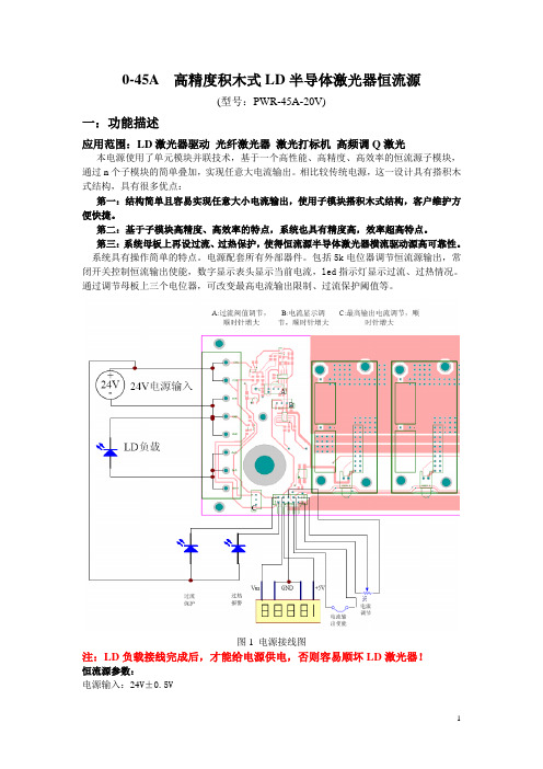
0-45A 高精度积木式LD半导体激光器恒流源(型号:PWR-45A-20V)一:功能描述应用范围:LD激光器驱动光纤激光器激光打标机高频调Q激光本电源使用了单元模块并联技术,基于一个高性能、高精度、高效率的恒流源子模块,通过n个子模块的简单叠加,实现任意大电流输出。
相比较传统电源,这一设计具有搭积木式结构,具有很多优点:第一:结构简单且容易实现任意大小电流输出,使用子模块搭积木式结构,客户维护方便快捷。
第二:基于子模块高精度、高效率的特点,系统也具有精度高,效率超高特点。
第三:系统母板上再设过流、过热保护,使得恒流源半导体激光器横流驱动源高可靠性。
系统具有操作简单的特点。
电源配套所有外部器件。
包括5k电位器调节恒流源输出,常闭开关控制恒流输出使能,数字显示表头显示当前电流,led指示灯显示过流、过热情况。
通过调节母板上三个电位器,可改变最高电流输出限制、过流保护阈值等。
图1 电源接线图注:LD负载接线完成后,才能给电源供电,否则容易顺坏LD激光器!恒流源参数:电源输入:24V±0.5V输入功率:1000W电源输出:0-45A电压输出:1-20V慢启动时间:500mS效率大于:92%电流显示:三位半数字显示过流、过热保护二:控制接口控制接口采用10芯IDC10接口,在线路板的左下角位置,参加图2所示。
图2 控制接口示意图下面分别介绍各个端口的功能:1脚:过热报警端口图3 过热报警接线图内部为npn三极管结构,外接LED指示灯,内部具有0.125W限流电阻,电源外部不必再添加限流电阻。
如果内部温度超过80度,过热报警动作,指示灯亮。
(电源正常工作)2脚:过流报警端口图4 过流报警接线图内部为SCR 结构,外接LED 指示灯,内部具有0.125W 限流电阻。
如果出现电源过流情况,过流保护动作,指示灯亮,电源停止输出。
3脚:+5V 输出端口该端口提供不超过100mA 的电流输出, 用于电流显示表头的正极供电。
常用运算放大器
返回
低噪声和精密的OP27 OP273 低噪声和精密的OP27-1
低噪声和精密的OP27 OP273 低噪声和精密的OP27-2
低噪声和精密的OP27 OP273 低噪声和精密的OP27-3
返回
低噪声、高速和精密的OP37 OP374 低噪声、高速和精密的OP37-1
低噪声、高速和精密的OP37 OP374 低噪声、高速和精密的OP37-2
低噪声、高速和精密的OP37 OP374 低噪声、高速和精密的OP37-3
低噪声、高速和精密的OP37 OP374 低噪声、高速和精密的OP37-4
返回
低噪声、高速和精密的OP37 OP374 低噪声、高速和精密的OP37-5
Hale Waihona Puke 速的LF353 LF3535 中速的LF353-1
中速的LF353 LF3535 中速的LF353-2
LM6164高速运算放大器 高速运算放大器9 LM6164高速运算放大器-6
返回
常见功率运算放大器10 常见功率运算放大器-1
18W功率运放TDA2030 18W功率运放TDA2030 功率运放
常见功率运算放大器10 常见功率运算放大器-2
常见功率运算放大器10 常见功率运算放大器-3
常见功率运算放大器10 常见功率运算放大器-4
LM6164高速运算放大器 高速运算放大器9 LM6164高速运算放大器-2
LM6164高速运算放大器 高速运算放大器9 LM6164高速运算放大器-3
LM6164高速运算放大器 高速运算放大器9 LM6164高速运算放大器-4
LM6164高速运算放大器 高速运算放大器9 LM6164高速运算放大器-5
常见仪表放大器AD620 AD62011 常见仪表放大器AD620-7
ICP DAS tM-7530 产品说明书
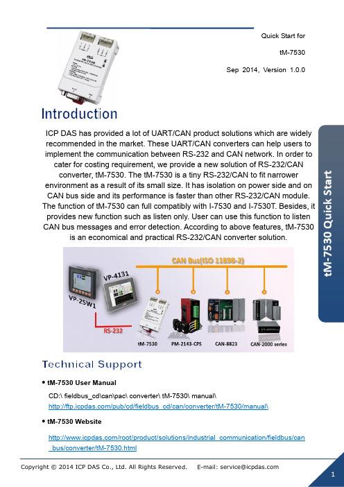
Quick Start fortM-7530Sep 2014, Version 1.0.0ICP DAS has provided a lot of UART/CAN product solutions which are widely recommended in the market. These UART/CAN converters can help users to implement the communication between RS-232 and CAN network. In order to cater for costing requirement, we provide a new solution of RS-232/CAN converter, tM-7530. The tM-7530 is a tiny RS-232/CAN to fit narrower environment as a result of its small size. It has isolation on power side and on CAN bus side and its performance is faster than other RS-232/CAN module. provides new function such as listen only. User can use this function to listen CAN bus messages and error detection. According to above features, tM-7530is an economical and practical RS-232/CAN converter solution.tM-7530 User ManualCD:\ fieldbus_cd\can\pac\ converter\ tM-7530\ manual\/pub/cd/fieldbus_cd/can/converter/tM-7530/manual\ tM-7530 Website/root/product/solutions/industrial_communication/fieldbus/cantM-7530 Utility/pub/cd/fieldbus_cd/can/converter/tM-7530/utilityICP DAS Website/1 -----------------------------------------------------------------------------------Hardware Introduction and InstallationThe left graph is the surface of tM-7530. It uses D-sub9 pin female connector as RS-232 communicationinterface and uses 2 or 3 wire to connect CAN buswith spring type connector. It has 2 LED indicatorsRun and Err. They are used to response modulestatus immediately at all time.Table: RS-232 Pin Assignment Table: Power and CAN Bus Pin AssignmentHow to connect with spring type connector? Press and Insert.2-----------------------------------------------------Configuration/Run ModeThere is a dip-switch on the bottom of tM-7530. After switching and rebooting, the tM-7530 will enter into Normal mode or Init mode.3-----------------------------------------------------tM-7530 wire connection4--------------------------------------Terminal Resistor5------------------------------------------------------------Software Utility IntroductionThere is no terminator resistor in the tM-7530. Therefore, if users would like to use terminator resistor, it is necessary to wire a 120Ω resistance on the CAN bus, as following figure.The tM-7530 uses VxCAN Utility to configure module and test. The VxCAN Utility is based on the Virtual CAN technology which is developed by the ICP DAS and is used to integrate the CAN interfaces of the different CAN converters from the ICP DAS. All of the CAN interfaces found by the PC will be sequentially mapping to the virtual CAN ports by the Virtual CAN driver. Users just use the virtual CAN ports to develop their application, and don ’t need to know what kind of6----------------------------------------------------------------------------Configure tM-7530 via VxCAN UtiliyBefore powering on the CAN converters, users must set them to the Init mode. Users need to switch the Init/Normal DIP-Switch to Init positionStep 3: Click the buttonThe configuration is divided to three areas with different color. They are UART, Communication, and CAN configuration area. Each area can set different parameters of tM-7530.After finishing the configuration, users can click the button “Save All Setting” to save the configuration in to the EEPROM of the CAN converter. If users would like to recover the parameters to the factory default, click “Load Default Setting” button to recover all of the configuration parameters to be default value. Afterwards, users can use the button “Save All Settings”to save the default parameters in to the EEPROM of the CAN converter.The default values of the parameters of the CAN converter are shown below.RS-232:RS-232 Baud rate = 115200Data Bit = 8Stop Bit = 1Parity = NoneAdd Checksum = NoError Response = NoTimeStamp Response = NoCAN:CAN Specification = 2.0ACAN bus Baud rate = 125KAcceptance Code = 000Acceptance Mask = 000Communication:7----------------------------------------------------------------Test tM-7530 via VxCAN UtiliySet the Init/Normal DIP switch of the CAN converter to normal mode. When the CAN module runs on the normal mode, the run LED indicator will be turned on. If the CAN converter sends or receives the CAN messages, the run LED will flash once per message.Step 3: Click the search buttonCheck the “Active Port ” and Click “Confirm ” button to enable the CAN port of the CAN converter. The parameters set here are not stored in the EEPROM. If users would like to configure the other parameters expect the CAN parameters, please use Configuration interface of the VxCAN Utility to do that.buttonThe test interface is divided to two areas. One is for sending CAN messages, and the other is for reception. If users want to send CAN message, fill the data into the corresponding field, and click “Send ” button. If the CAN converter gets any CAN messages, they will be shown in received area automatically. About the details for the VxCAN Utility operation please refer to the users ’ manual of the VxCAN Utility in the following web site.。
激光头代换大全

激光头代换大全激光头是打印机中非常重要的部件,它直接影响着打印机的打印质量和寿命。
随着科技的不断发展,激光头的种类和品牌也越来越多样化,因此在选择激光头时需要格外注意。
本文将为大家介绍一些常见的激光头品牌和型号,帮助大家更好地了解激光头的选择和更换。
首先,我们来介绍一些常见的激光头品牌。
惠普(HP)作为全球知名的打印机品牌,其激光头质量和稳定性备受认可。
佳能(Canon)也是一家值得信赖的品牌,其激光头在打印速度和精度方面表现出色。
爱普生(Epson)的激光头则以其耐用性和经济性而受到广泛好评。
除此之外,还有一些其他品牌的激光头也备受关注,比如联想、戴尔等,它们都有各自的特点和优势。
其次,让我们来看看一些常见的激光头型号。
在HP品牌中,常见的激光头型号有HP 12A、HP 85A等,它们适用于不同型号的HP打印机,用户在更换激光头时需要根据自己的打印机型号进行选择。
而在佳能品牌中,常见的激光头型号有CRG-328、CRG-925等,这些型号的激光头适用于佳能的不同打印机系列。
在选择激光头时,用户需要注意型号的匹配性,以确保激光头能够正常使用。
除了品牌和型号,激光头的更换时间也是非常重要的。
一般来说,激光头的寿命在使用一定时间后会出现打印质量下降的情况,这时就需要考虑更换激光头了。
一般来说,打印机厂家会在打印机的使用手册中标明激光头的预期寿命,用户可以根据这个时间来进行更换。
另外,如果在打印过程中出现打印质量明显下降的情况,也可以考虑更换激光头,以恢复打印质量。
在更换激光头时,用户需要注意一些细节。
首先,要选择正规渠道购买的激光头,以确保质量和售后服务。
其次,更换激光头时需要按照打印机厂家的操作指南进行,避免因操作不当导致损坏打印机。
最后,更换激光头后,用户需要进行打印质量的测试,以确保新的激光头能够正常工作。
总的来说,激光头是打印机中非常重要的部件,选择合适的品牌和型号,以及注意更换的时间和细节,都是保证打印机正常工作和打印质量的关键。
八脚电源管理芯片通用型号

八脚电源管理芯片通用型号
200A6 200D6 203D6 DAP02A DAP08A DAP02ALSZ 通用
液晶品牌与型号电源管理芯片型号与封装可代换型号
BENQ 71G+ 1200AP40 直插 1200AP10 1200AP60
AOC 712SI EA1532A贴片
三星型号忘记 DM0565R
优派型号忘记 TOP245YN
LG型号忘记 FAN7601
飞利浦170s6 dap02alsz 贴片(2楼说的)
LG型号忘记 FAN7601 可以用LAF0001代
飞利浦170s6 dap02alsz=sg6841
HP17驱动高压电源全一体 SG5841SZ贴片,可用SG6841DZ 代用。
联想后来出的像IBM的17的,SG6841DZ 可用SG6841D代用(我亲自试过的)
三星型号忘记 DM0565R(有好几款都采用这一个PWM IC的)三星型号忘记 DM0465R(我记得还有这么一款的,
其他我知道的常用型号有
SG6841DZ 贴片很多机器上用到
SG5841SZ 贴片用SG6841DZ可以代用,
DAP8A 与203D6可代用(我没试过)
还有LD7575可用203D6代用,只是1脚的对地电阻不同,LD7575是100K,203D6是24.1K,LP7552可用SG6841代用
DAP02ALSZ与SG6841S可以互换。
SM7530 (20-50V)600mA原边反馈LED恒流驱动控制芯片

一、线圈绕制表 绕组 挡墙(mm) 脚 编号 底 顶 Np1 Ns Na Np2 位 线规*股数 圈数
mm*P TS
绕向
胶带规格 层数
mቤተ መጻሕፍቲ ባይዱ TS
绕制方法
备注
4—>2 Φ0.35*1 12—>8 Φ0.45*1 6—>5 Φ0.17*1 2—>1 Φ0.45*1
25 52 24 42
顺 顺 顺 顺
密绕 密绕 密绕 密绕 三层绝缘线
管脚图
应用领域
T5、T8 日光灯 吸顶灯、平板灯等 DC/DC 或 AC/DC 的 LED 驱动器 LED 信号灯和装饰灯 SOT23-6
典型示意电路图
SM7530 高功率因数 LED 恒流驱动芯片 v1.6
变压器规格书
客 户 PC40 产品型号/名称 PQ2620变压器 磁 芯 型 号 PQ2620 骨 磁芯材质 架 生产编号:V1.0-N SM7530 20V-50V/600mA PQ2620(6+6)立式
型号描述
FUS-RST-2A-250V VAR-Φ10-470V-Φ10D471K CAP-CX-100.00nF-275V L-0.33mH-12.7mm*7.9mm*4mm L-12.0mH-UU9.8 L-2.4mH-Ф8*10(饱和电流>250mA) CAP-CY-2.2nF-10%-250V BR-3.00A-1000V-KBP307
概述
SM7530 是一款单级、带有源高功率因数校正的高精度高效率的原 边反馈 LED 恒流驱动控制芯片。采用我司的恒流控制技术,输入无需 电解电容。适用于 85Vac~265Vac 全范围输入电压,恒流精度可达到± 5% ,PF 值大于 0.9。 SM7530 主要适用于高亮的 LED 驱动器,可实现高功率因素和恒定 的输出电流。外围器件少,方案成本低,具有输出开、短路保护特性。 可通过 EFT、雷击浪涌等可靠性测试,亦可通过 3C、UL、CE 等认证标 准。
士兰微电子SD7530 LED照明高功率因数反激式PWM控制器说明书

高功率因数反激式PWM控制器
日光灯
产品规格分类
产品名称 封装形式 打印名称 材料 包装
无铅料管SD7530 DIP-8-300-2.54
SD7530
无铅料管
SD7530S
SD7530S SOP-8-225-1.27
无铅编带SD7530STR SOP-8-225-1.27
SD7530S
内部框图
40
OL -600/800
误差
放大器
比较器
SD7530说明书
电气参数 (除非特别指定,V
CC
=22V;C O=1nF;-25°C<T amb<125°C)
TEL 158********
SD7530说明书
TEL 158********
管脚描述
封装外形图
SD7530说明书
MOS电路操作注意事项:
静电在很多地方都会产生,采取下面的预防措施,可以有效防止MOS电路由于受静电放电影响而引起的损坏:
• 操作人员要通过防静电腕带接地。
• 设备外壳必须接地。
• 装配过程中使用的工具必须接地。
• 必须采用导体包装或抗静电材料包装或运输。
声明:
•士兰保留说明书的更改权,恕不另行通知!客户在下单前应获取最新版本资料,并验证相关信息是否完整和最新。
•任何半导体产品特定条件下都有一定的失效或发生故障的可能,买方有责任在使用Silan产品进行系统设计和整机制造时遵守安全标准并采取安全措施,以避免潜在失败风险可能造成人身伤害或财产损
失情况的发生!
•产品提升永无止境,我公司将竭诚为客户提供更优秀的产品!
TEL 158********。
LD7530

CS Current sense pin, connect to sense the MOSFET current VCC Supply voltage pin OUT Gate drive output to drive the external MOSFET
LD7530/LD7530A
Electrical Characteristics
(TA = +25oC unless otherwise stated, VCC=15.0V)
PARAMETER
CONDITIONS
Supply Voltage (Vcc Pin)
Startup Current
Operating Current (with 1nF load on OUT pin)
Recommended Operating Conditions
Item
Min.
Max.
Unit
Supply Voltage Vcc (LD7530)
11
25
V
Supply Voltage Vcc (LD7530A)
11
18
V
CT Value
0.047
0.1
μF
5
Leadtrend Technology Corporation LD7530&LD7530A-DS-04 December 2007
FUNCTION
GND Ground Voltage feedback pin (same as the COMP pin in UC384X), by connecting
- 1、下载文档前请自行甄别文档内容的完整性,平台不提供额外的编辑、内容补充、找答案等附加服务。
- 2、"仅部分预览"的文档,不可在线预览部分如存在完整性等问题,可反馈申请退款(可完整预览的文档不适用该条件!)。
- 3、如文档侵犯您的权益,请联系客服反馈,我们会尽快为您处理(人工客服工作时间:9:00-18:30)。
Absolute Maximum Ratings
Supply Voltage VCC COMP, CT, CS Junction Temperature Operating Ambient Temperature Storage Temperature Range Package Thermal Resistance (SOT-26) Package Thermal Resistance (DIP-8) Power Dissipation (SOT-26, at Ambient Temperature = 85°C) Power Dissipation (DIP-8, at Ambient Temperature = 85°C) Lead temperature (Soldering, 10sec) ESD Voltage Protection, Human Body Model ESD Voltage Protection, Machine Model Gate Output Current
VCOMP=0V VCOMP=3V Protection tripped (OLP, OVP)
UVLO (off)
UVLO (on)
OVP Level
LD7530 LD7530A
Voltage Feedback (Comp Pin)
Short Circuit Current Open Loop Voltage
And to satisfy different designs, 2 versions of OVP levels are implemented as ---
z LD7530 --- 28.0V ± 1.2V.
z LD7530A --- 21.0V ± 1.2V.
Features
z High-Voltage CMOS Process with Excellent ESD protection
Blanking
+ 0.85V
PWM Comparator
Slope Compensation
OCP Comparator
5.0V
OLP Delay Counter
OVP OLP
OLP
Comparator
PG
OLP Delay
SQ R
Protection
SQ R
GND
4
Leadtrend Technology Corporation LD7530&LD7530A-DS-02a May 2007
LD7530/LD7530A
30V -0.3 ~7V 150°C -40°C to 85°C -65°C to 150°C 250°C/W 100°C/W 250mW 650mW 260°C 2.5 KV 250 V 300mA
Caution: Stresses beyond the ratings specified in “Absolute Maximum Ratings” may cause permanent damage to the device. This is a stress only rating and operation of the device at these or any other conditions above those indicated in the operational sections of this specification is not implied.
Shipping 3000 /tape & reel 3600 /tube /Carton 3000 /tape & reel 3600 /tube /Carton
2
Leadtrend Technology Corporation LD7530&LD7530A-DS-02a May 2007
LD7530/LD7530A
& Vref
OVP Comparator
CT
Trembling
PG
OSC
OLP
Vref OK
OVP
28.0V(LD7530)
Delay
21.0V(LD7530A)
65KHz OSC
Protection
Driver Stage
OUT
Green-Mode Control
COMP CS
2R
R
∑+
Leading Edge
LD7530/LD7530A
Electrical Characteristics
(TA = +25oC unless otherwise stated, VCC=15.0V)
PARAMETER
CONDITIONS
Supply Voltage (Vcc Pin)
Startup Current
Operating Current (with 1nF load on OUT pin)
LD7530/LD7530A
Pin Configuration (LD7530)
DIP-8 (TOP VIEW)
SOT-26 (TOP VIEW)
GND COM P NC CT
8 765
TOP MARK YYWW##
OUT VCC CS
6
5
4
Y WP 30
1
2
3
OUT VCC
NC CS
1 234
GND COMP CT
Pin Configuration (LD7530A)
DIP-8 (TOP VIEW)
SOT-26 (TOP VIEW)
GND COM P NC CT
8 765
TOP MARK YYWW##
OUT VCC CS
6
5
4
Y WP 30A
1
2
3
1 234
GND COMP CT
Y The PB free package is identified in embossed font
Applications
z Switching AC/DC Adaptor and Battery Charger z Open Frame Switching Power Supply
Typical Application
1
Leadtrend Technology Corporation LD7530&LD7530A-DS-02a May 2007
3
Leadtrend Technology Corporation LD7530&LD7530A-DS-02a May 2007
Block Diagram
LD7530/LD7530A
VCC
32V
UVLO Comparator
All
internal bias Blocks
16.0V/ 10.0V
VCC OK
VCOMP=0V COMP pin open
Green Mode Threshold VCOMP
Current Sensing (CS Pin)
Maximum Input Voltage, Vcs(off)
Leading Edge Blanking Time
Input impedance
Delay to Output
Package
TOP MARK
LD7530 PL
SOT-26
YWP/30
LD7530 PN
DIPSOT-26
YWP/30A
LD7530A PN
DIP-8
LD7530APN
Note: The LD7530 and LD7530A are ROHS compliant.
Recommended Operating Conditions
Item
Min.
Max.
Unit
Supply Voltage Vcc (LD7530)
11
25
V
Supply Voltage Vcc (LD7530A)
11
18
V
CT Value
0.047
0.1
µF
5
Leadtrend Technology Corporation LD7530&LD7530A-DS-02a May 2007
Furthermore, the frequency trembling function is to reduce the noise level and thus helps the power circuit designers to easily deal with the EMI filter design by using minimum component cost and developing time.
z Very Low Startup Current (<20µA) z Current Mode Control z Non-audible-noise Green Mode Control z UVLO (Under Voltage Lockout) z LEB (Leading-Edge Blanking) on CS Pin z Programmable Modulating Frequency for Trembling z Internal Slope Compensation z OVP (Over Voltage Protection) on Vcc Pin z OLP (Over Load Protection) z 300mA Driving Capability
LD7530/LD7530A
5/18/2007
Green-Mode PWM Controller with Frequency Trembling and Integrated Protections