HopeRF_新品推荐-带RF功能单芯片SOC方案RF60
芯海科技 ARM M M0-based MCU 输出手册说明书

输出手册版本历史版本号说明日期1.0 初版2019-6-171.1 1. LRC频率:min(30->27),max(50->62)2. ADC特性更新: fADC-40℃≤ Trange ≤ 85℃,fADC≤14MHz,支持电压范围2.65≤ VDDA ≤5.5V;-40℃≤ Trange ≤ 105℃,fADC≤14MHz,支持电压范围2.7≤ VDDA ≤5.5V;-40℃≤ Trange ≤ 105℃,fADC≤12MHz,支持电压范围2.4≤ VDDA ≤5.5V;进入校准模式,fADC≤12MHz。
进入正常转换模式,fADC≤14MHz。
支持:-40℃≤ Trange ≤ 105℃和电压范围2.4≤ VDDA ≤5.5V;3. ADC特性更新:VDDA=2.4V时,Offset和ERR Gain更新2020-6-31.2 1.增加G6U6版本相关信息2020-6-191.3 1.更新温度传感器线性度参数,区分不同温度范围2020-8-262/56文件编号:CS-QR-YF-054A02目录输出手册版本历史 (2)目录 (3)1介绍 (5)2功能 (6)3器件一览 (8)4引脚描述 (10)4.1LQFP48 (10)4.2LQFP32 (10)4.3QFN28L (11)4.4TSSOP20 (11)4.5引脚描述 (12)5I/O 复用 (15)5.1PA口复用功能 (15)5.2PB口复用功能 (16)6存储器 (17)7功能描述 (21)7.1ARM®C ORTEX®-M0内核 (21)7.2存储器 (21)7.3时钟 (21)7.4工作环境 (23)7.4.1工作电压 (23)7.5启动模式 (23)7.6电源管理 (23)7.6.1低功耗模式 (23)7.6.2RTC和备用寄存器的电源电压VBAT (23)7.6.3上电复位/掉电复位(POR/PDR) (23)7.6.4低电压复位模块(LVD) (24)7.7通用输入输出端口(I/O) (24)7.8模数转换器(ADC) (24)7.8.1温度传感器(TS) (24)7.8.2内部参考电压 (24)7.8.3VBAT监测 (25)7.9定时器 (25)7.9.1高级定时器 (TIM1) (25)7.9.2通用定时器 (TIM3, 14, 15,16, 17) (25)7.9.3基本定时器(TIM6) (26)7.9.4独立看门狗定时器(FWDT) (26)7.9.5窗看门狗定时器(WWDT) (26)7.9.6滴答定时器(SysTick) (26)7.10直接内存存取(DMA) (26)3/56文件编号:CS-QR-YF-054A027.11中断和事件 (26)7.12实时时钟(RTC)和备用寄存器 (26)7.13串行外设总线(SPI)/集成电路内置音频总线(I2S) (27)7.14通用同步异步收发器(USART) (27)7.15内置集成电路接口(I2C) (29)7.16循环冗余校验 (29)7.17串行调试端口(SWD-DP) (29)8电气特性 (30)8.1说明 (30)8.2绝对最大额定值 (31)8.3工作条件 (31)8.4I/O端口特性 (32)8.5低功耗模式唤醒时间 (33)8.6RC振荡特性 (33)8.7晶振特性 (34)8.8外部时钟特性 (36)8.9PLL特性 (36)8.10功耗 (37)8.11内部参考电压特性 (38)8.12ADC特性 (38)8.13温度传感器特性 (39)8.14VBAT监测器特性 (39)8.15F LASH 特性 (39)8.16定时器特性 (40)8.17SPI/I2S特性 (40)8.18I2C特性 (44)8.19ESD特性 (44)9封装信息 (46)9.1LQFP48 (46)9.2LQFP32 (48)9.3QFN28L (49)9.4TSSOP20 (51)10订货信息 (52)11勘误表 (53)12缩略语 (54)13销售和服务 (56)4/56文件编号:CS-QR-YF-054A021介绍CS32F030系列微控制器采用高性能的32位ARM® Cortex®-M0 内核,嵌入高达64Kbytes flash和8Kbytes SRAM,最高工作频率48MHz。
费思FT6300A系列中小功率电子负载用户手册适用型号(FT6301A-FT6306A)

安全摘要
在操作和维修电子负载过程中,请严格遵守以下安全须知。不遵守以下注意事项或本手册中其它章节 提示的特定警告,可能会削弱本负载所提供的保护功能。对于用户不遵守这些注意事项而造成的后果,费 思科技不负任何责任。
目录 ....................................................................................................................................................... IV
II
安全标识
在本产品外壳、用户手册所使用国际符号的解释请参见下表。
III
目录
前言........................................................................................................................................... I 通告........................................................................................................................................... I
第 2 章 安装.......................................................................................................................................... 11
Silicon Labs EFR32BG21B Gecko 无线 SoC 产品系列介绍说明书
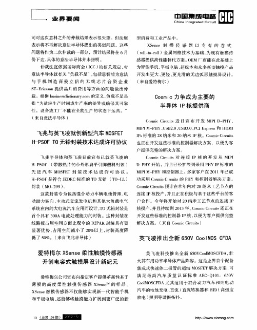
EFR32BG21B Gecko 无线 SoC 产品系列数据表EFR32BG21B SoC 是无线 Gecko 产品组合的组成部分。
EFR32BG21BSoC 是实现 IoT 设备上节能 Bluetooth 5 连网的理想之选。
这款单芯片解决方案结合了 80 MHz ARM Cortex-M33 和高性能 2.4 GHz 无线电,以及集成的 硬件安全引擎,旨在为 IoT 连接应用提供高度安全且节能的无线 SoC 。
EFR32BG21B 应用包括:主要特点•32 位 ARM® Cortex®-M33 内核,最高工作频率为 80 MHz•最高 1024 kB 闪存和 96 kB RAM •12 信道外围设备反射系统,可实现 MCU 外围设备的自主交互•集成 PA ,TX 功率高达 20 dBm (2.4 GHz)•强大的外围设备,4x4 QFN 封装内多达 20个 GPIO•照明•联网家庭•网关和数字助手•建筑自动化及安全EM4—ShutoffEM3—StopEM2—Deep SleepEM1—SleepEM0—Active| Building a more connected world.Rev. 1.01. 功能列表下方列出了 EFR32BG21B 的特色功能。
•低功耗无线片上系统•高性能 32 位 80 MHz ARM Cortex®-M33,带有 DSP 指令和浮点单元,可高效处理信号•高达 1024 kB 的闪存程序存储器•高达 96 kB 的 RAM 数据存储器•2.4 GHz 无线电操作•TX 功耗高达 20 dBm•低能耗•8.8 2.4 GHz 时 mA RX 电流 (1 Mbps GFSK)•9.32.4 GHz 和 0 dBm 输出功率时 mA TX 电流•33.8 2.4 GHz 和 10 dBm 输出功率时 mA TX 电流•50.9 主动模式 (EM0) 下 μA/MHz•5.0 μA EM2 深度睡眠电流(96 kB RAM 保留和通过 LFRCO 运行的 RTC)•4.5 μA EM2 深度睡眠电流(16 kB RAM 保留和通过 LFRCO 运行的 RTC)•高接收器性能•-97.5 dBm 灵敏度 @ 1 Mbit/s GFSK•-94.4 dBm 灵敏度 @ 2 Mbit/s GFSK•-104.9 dBm 灵敏度 @ 125 kbps GFSK•支持的调制格式•GFSK•协议支持•蓝牙低功耗 (Bluetooth 5)•可广泛选择的 MCU 外围设备•12 位 1 Msps SAR 模数转换器 (ADC)•2 个模拟比较器 (ACMP)•最多 20 个通用 I/O 引脚,具有输出状态保持和异步中断功能•8 信道 DMA 控制器•12 信道外围反射系统 (PRS)•3 个 16 位定时器/计数器•3 个比较/捕获/PWM 信道•1 个 32 位定时器/计数器•3 个比较/捕获/PWM 信道•32 位实时计数器•24 位低功耗定时器,用于产生波形•2 个看门狗定时器•3 个通用同步/异步接收器/发送器 (UART/SPI/SmartCard(ISO 7816)/IrDA/I2S)•2 个 I2C 接口,支持 SMBus•广泛的工作范围•1.71 V 至 3.8 V 单电源•-40°C 至 125°C 环境温度•Secure Vault•AES128/192/256、ChaCha20-Poly1305、SHA-1、SHA-2/256/384/512、ECDSA+ECDH(P-192、P-256、P-384、P-521)、Ed25519 和 Curve25519、J-PAKE、PBKDF2 的硬件加密加速•真随机数发生器 (TRNG)•ARM® TrustZone®•安全启动(根信任安全加载程序)•全调试解锁•DPA 对策•使用 PUF 进行安全密钥管理•防篡改•安全证明•QFN32 4x4 mm 封装•0.4 mm 间距EFR32BG21B Gecko 无线 SoC 产品系列数据表功能列表EFR32BG21B Gecko Wireless SoC Family Data SheetOrdering Information 2. Ordering InformationTable 2.1. Ordering Information | Building a more connected world.Rev. 1.0 | 3Table of Contents1. Feature List (2)2. Ordering Information (3)3. System Overview (7)3.1 Introduction (7)3.2 Radio (7)3.2.1 Antenna Interface (7)3.2.2 Fractional-N Frequency Synthesizer (8)3.2.3 Receiver Architecture (8)3.2.4 Transmitter Architecture (8)3.2.5 Packet and State Trace (8)3.2.6 Data Buffering (8)3.2.7 Radio Controller (RAC) (8)3.3 General Purpose Input/Output (GPIO) (9)3.4 Clocking (9)3.4.1 Clock Management Unit (CMU) (9)3.4.2 Internal and External Oscillators (9)3.5 Counters/Timers and PWM (9)3.5.1 Timer/Counter (TIMER) (9)3.5.2 Low Energy Timer (LETIMER) (9)3.5.3 Real Time Clock with Capture (RTCC) (10)3.5.4 Back-Up Real Time Counter (BURTC) (10)3.5.5 Watchdog Timer (WDOG) (10)3.6 Communications and Other Digital Peripherals (10)3.6.1 Universal Synchronous/Asynchronous Receiver/Transmitter (USART) (10)3.6.2 Inter-Integrated Circuit Interface (I2C) (10)3.6.3 Peripheral Reflex System (PRS) (10)3.7 Secure Vault High Features (10)3.7.1 Secure Boot with Root of Trust and Secure Loader (RTSL) (11)3.7.2 Cryptographic Accelerator (11)3.7.3 True Random Number Generator (11)3.7.4 Secure Debug with Lock/Unlock (11)3.7.5 DPA Countermeasures (11)3.7.6 Secure Key Management with PUF (12)3.7.7 Anti-Tamper (12)3.7.8 Secure Attestation (12)3.8 Analog (12)3.8.1 Analog Comparator (ACMP) (12)3.8.2 Analog to Digital Converter (IADC) (12)3.9 Reset Management Unit (RMU) (12)3.10 Core and Memory (13)3.10.1 Processor Core (13)3.10.2 Memory System Controller (MSC) (13)3.10.3 Linked Direct Memory Access Controller (LDMA) (13)3.11 Memory Map (14)3.12 Configuration Summary (15)4. Electrical Specifications (16)4.1 Electrical Characteristics (16)4.1.1 Absolute Maximum Ratings (17)4.1.2 General Operating Conditions (18)4.1.3 Thermal Characteristics (19)4.1.4 Current Consumption (20)4.1.5 2.4 GHz RF Transceiver Characteristics (25)4.1.6 Flash Characteristics (38)4.1.7 Wake Up, Entry, and Exit times (39)4.1.8 Oscillators (40)4.1.9 GPIO Pins (3V GPIO pins) (45)4.1.10 Analog to Digital Converter (ADC) (46)4.1.11 Analog Comparator (ACMP) (48)4.1.12 Temperature Sense (49)4.1.13 Brown Out Detectors (50)4.1.14 USART SPI Master Timing (52)4.1.15 USART SPI Slave Timing (54)4.1.16 I2C Electrical Specifications (55)4.1.17 Boot Timing (57)4.1.18 Crypto Operation Timing for SE Manager API (58)4.1.19 Crypto Operation Average Current for SE Manager API (60)4.2 Typical Performance Curves (62)4.2.1 Supply Current (63)4.2.2 2.4 GHz Radio (65)5. Typical Connection Diagrams (67)5.1 Power (67)5.2 RF Matching Networks (67)5.2.1 2.4 GHz 0 dBm Matching Network (68)5.2.2 2.4 GHz 10 dBm Matching Network (69)5.2.3 2.4 GHz 20 dBm Matching Network (69)5.3 Other Connections (70)6. Pin Definitions (71)6.1 QFN32 2.4GHz Device Pinout (71)6.2 Alternate Function Table (72)6.3 Analog Peripheral Connectivity (73)6.4 Digital Peripheral Connectivity (74)7. QFN32 Package Specifications (77)7.1 QFN32 Package Dimensions (77)7.2 QFN32 PCB Land Pattern (79)7.3 QFN32 Package Marking (81)8. Revision History (82)3. System Overview3.1 IntroductionThe EFR32 product family combines an energy-friendly MCU with a high performance radio transceiver. The devices are well suited for secure connected IoT multiprotocol devices requiring high performance and low energy consumption. This section gives a short intro-duction to the full radio and MCU system. The detailed functional description can be found in the EFR32xG21 Reference Manual.A block diagram of the EFR32BG21B family is shown in Figure 3.1 Detailed EFR32BG21B Block Diagram on page 7. The diagram shows a superset of features available on the family, which vary by OPN. For more information about specific device features, consult Ordering Information .RESETnDVDDAVDD PAVDD RFVDD DECOUPLEIOVDD PDnPCnPBnPAnRF2G4_IO1RF2G4_IO2Figure 3.1. Detailed EFR32BG21B Block Diagram3.2 RadioThe EFR32BG21B features a highly configurable radio transceiver supporting the Bluetooth Low Energy wireless protocol.3.2.1 Antenna InterfaceThe 2.4 GHz antenna interface consists of two single-ended pins (RF2G4_IO1 and RF2G4_IO2) that interface directly to two LNAs and two 10 dBm PAs. For devices that support 20 dBm, these pins also interface to the 20 dBm on-chip balun. Integrated switches select either RF2G4_IO1 or RF2G4_IO2 to be the active path.The external components and power supply connections for the antenna interface typical applications are shown in the RF Matching Networks section.Rev. 1.0 | 73.2.2 Fractional-N Frequency SynthesizerThe EFR32BG21B contains a high performance, low phase noise, fully integrated fractional-N frequency synthesizer. The synthesizer is used in receive mode to generate the LO frequency for the down-conversion mixer. It is also used in transmit mode to directly gener-ate the modulated RF carrier.The fractional-N architecture provides excellent phase noise performance, frequency resolution better than 100 Hz, and low energy consumption. The synthesizer’s fast frequency settling allows for very short receiver and transmitter wake up times to reduce system energy consumption.3.2.3 Receiver ArchitectureThe EFR32BG21B uses a low-IF receiver architecture, consisting of a Low-Noise Amplifier (LNA) followed by an I/Q down-conversion mixer. The I/Q signals are further filtered and amplified before being sampled by the IF analog-to-digital converter (IFADC).The IF frequency is configurable from 150 kHz to 1371 kHz. The IF can further be configured for high-side or low-side injection, provid-ing flexibility with respect to known interferers at the image frequency.The Automatic Gain Control (AGC) module adjusts the receiver gain to optimize performance and avoid saturation for excellent selec-tivity and blocking performance. The 2.4 GHz radio is calibrated at production to improve image rejection performance.Demodulation is performed in the digital domain. The demodulator performs configurable decimation and channel filtering to allow re-ceive bandwidths ranging from 0.1 to 2530 kHz. High carrier frequency and baud rate offsets are tolerated by active estimation and compensation. Advanced features supporting high quality communication under adverse conditions include forward error correction by block and convolutional coding as well as Direct Sequence Spread Spectrum (DSSS).A Received Signal Strength Indicator (RSSI) is available for signal quality metrics, for level-based proximity detection, and for RF chan-nel access by Collision Avoidance (CA) or Listen Before Talk (LBT) algorithms. An RSSI capture value is associated with each received frame and the dynamic RSSI measurement can be monitored throughout reception.3.2.4 Transmitter ArchitectureThe EFR32BG21B uses a direct-conversion transmitter architecture. For constant envelope modulation formats, the modulator controls phase and frequency modulation in the frequency synthesizer. Transmit symbols or chips are optionally shaped by a digital shaping filter. The shaping filter is fully configurable, including the BT product, and can be used to implement Gaussian or Raised Cosine shap-ing.Carrier Sense Multiple Access - Collision Avoidance (CSMA-CA) or Listen Before Talk (LBT) algorithms can be automatically timed by the EFR32BG21B. These algorithms are typically defined by regulatory standards to improve inter-operability in a given bandwidth be-tween devices that otherwise lack synchronized RF channel access.3.2.5 Packet and State TraceThe EFR32BG21B Frame Controller has a packet and state trace unit that provides valuable information during the development phase. It features:•Non-intrusive trace of transmit data, receive data and state information•Data observability on a single-pin UART data output, or on a two-pin SPI data output•Configurable data output bitrate / baudrate•Multiplexed transmitted data, received data and state / meta information in a single serial data stream3.2.6 Data BufferingThe EFR32BG21B features an advanced Radio Buffer Controller (BUFC) capable of handling up to 4 buffers of adjustable size from 64 bytes to 4096 bytes. Each buffer can be used for RX, TX or both. The buffer data is located in RAM, enabling zero-copy operations.3.2.7 Radio Controller (RAC)The Radio Controller controls the top level state of the radio subsystem in the EFR32BG21B. It performs the following tasks:•Precisely-timed control of enabling and disabling of the receiver and transmitter circuitry•Run-time calibration of receiver, transmitter and frequency synthesizer•Detailed frame transmission timing, including optional LBT or CSMA-CA3.3 General Purpose Input/Output (GPIO)EFR32BG21B has up to 20 General Purpose Input/Output pins. Each GPIO pin can be individually configured as either an output or input. More advanced configurations including open-drain, open-source, and glitch-filtering can be configured for each individual GPIO pin. The GPIO pins can be overridden by peripheral connections, like SPI communication. Each peripheral connection can be routed to several GPIO pins on the device. The input value of a GPIO pin can be routed through the Peripheral Reflex System to other peripher-als. The GPIO subsystem supports asynchronous external pin interrupts.All of the pins on ports A and port B are EM2 capable. These pins may be used by Low-Energy peripherals in EM2/3 and may also be used as EM2/3 pin wake-ups. Pins on ports C and D are latched/retained in their current state when entering EM2 until EM2 exit upon which internal peripherals could once again drive those pads.A few GPIOs also have EM4 wake functionality. These pins are listed in .3.4 Clocking3.4.1 Clock Management Unit (CMU)The Clock Management Unit controls oscillators and clocks in the EFR32BG21B. Individual enabling and disabling of clocks to all pe-ripheral modules is performed by the CMU. The CMU also controls enabling and configuration of the oscillators. A high degree of flexi-bility allows software to optimize energy consumption in any specific application by minimizing power dissipation in unused peripherals and oscillators.3.4.2 Internal and External OscillatorsThe EFR32BG21B supports two crystal oscillators and fully integrates five RC oscillators, listed below.• A high frequency crystal oscillator (HFXO) with integrated load capacitors, tunable in small steps, provides a precise timing refer-ence for the MCU and RF synthesizer. The HFXO provides excellent RF clocking performance using a 38.4 MHz crystal. The HFXO can also support an external clock source such as a TCXO for applications that require an extremely accurate clock frequency over temperature.• A 32.768 kHz crystal oscillator (LFXO) provides an accurate timing reference for low energy modes.•An integrated high frequency RC oscillator (HFRCO) is available for the MCU system, when crystal accuracy is not required. The HFRCO employs fast start-up at minimal energy consumption combined with a wide frequency range, from 1 MHz to 80 MHz.•An integrated high frequency RC oscillator (HFRCOEM2) runs down to EM2 and is available for timing the general-purpose ADC and the Serial Wire Viewer port with a wide frequency range.•An integrated fast start-up RC oscillator (FSRCO) that runs at a fixed 20 MHz•An integrated low frequency 32.768 kHz RC oscillator (LFRCO) for low power operation where high accuracy is not required.•An integrated ultra-low frequency 1 kHz RC oscillator (ULFRCO) is available to provide a timing reference at the lowest energy con-sumption in low energy modes.3.5 Counters/Timers and PWM3.5.1 Timer/Counter (TIMER)TIMER peripherals keep track of timing, count events, generate PWM outputs and trigger timed actions in other peripherals through the Peripheral Reflex System (PRS). The core of each TIMER is a 16-bit or 32-bit counter with up to 3 compare/capture channels. Each channel is configurable in one of three modes. In capture mode, the counter state is stored in a buffer at a selected input event. In compare mode, the channel output reflects the comparison of the counter to a programmed threshold value. In PWM mode, the TIMER supports generation of pulse-width modulation (PWM) outputs of arbitrary waveforms defined by the sequence of values written to the compare registers. In addition some timers offer dead-time insertion.See 3.12 Configuration Summary for information on the feature set of each timer.3.5.2 Low Energy Timer (LETIMER)The unique LETIMER is a 24-bit timer that is available in energy mode EM0 Active, EM1 Sleep, EM2 Deep Sleep, and EM3 Stop. This allows it to be used for timing and output generation when most of the device is powered down, allowing simple tasks to be performed while the power consumption of the system is kept at an absolute minimum. The LETIMER can be used to output a variety of wave-forms with minimal software intervention. The LETIMER is connected to the Peripheral Reflex System (PRS), and can be configured to start counting on compare matches from other peripherals such as the Real Time Clock.3.5.3 Real Time Clock with Capture (RTCC)The Real Time Clock with Capture (RTCC) is a 32-bit counter providing timekeeping down to EM3. The RTCC can be clocked by any of the on-board low-frequency oscillators, and it is capable of providing system wake-up at user defined intervals.A secondary RTC is used by the RF protocol stack for event scheduling, leaving the primary RTCC block available exclusively for appli-cation software.3.5.4 Back-Up Real Time Counter (BURTC)The Back-Up Real Time Counter (BURTC) is a 32-bit counter providing timekeeping in all energy modes, including EM4. The BURTC can be clocked by any of the on-board low-frequency oscillators, and it is capable of providing system wake-up at user defined inver-vals.3.5.5 Watchdog Timer (WDOG)The watchdog timer can act both as an independent watchdog or as a watchdog synchronous with the CPU clock. It has windowed monitoring capabilities, and can generate a reset or different interrupts depending on the failure mode of the system. The watchdog can also monitor autonomous systems driven by the Peripheral Reflex System (PRS).3.6 Communications and Other Digital Peripherals3.6.1 Universal Synchronous/Asynchronous Receiver/Transmitter (USART)The Universal Synchronous/Asynchronous Receiver/Transmitter is a flexible serial I/O module. It supports full duplex asynchronous UART communication with hardware flow control as well as RS-485, SPI, MicroWire and 3-wire. It can also interface with devices sup-porting:•ISO7816 SmartCards•IrDA•I2S3.6.2 Inter-Integrated Circuit Interface (I2C)The I2C module provides an interface between the MCU and a serial I2C bus. It is capable of acting as both a master and a slave and supports multi-master buses. Standard-mode, fast-mode and fast-mode plus speeds are supported, allowing transmission rates from 10 kbit/s up to 1 Mbit/s. Slave arbitration and timeouts are also available, allowing implementation of an SMBus-compliant system. The interface provided to software by the I2C module allows precise timing control of the transmission process and highly automated trans-fers. Automatic recognition of slave addresses is provided in active and low energy modes. Note that not all instances of I2C are avalia-ble in all energy modes.3.6.3 Peripheral Reflex System (PRS)The Peripheral Reflex System provides a communication network between different peripheral modules without software involvement. Peripheral modules producing Reflex signals are called producers. The PRS routes Reflex signals from producers to consumer periph-erals which in turn perform actions in response. Edge triggers and other functionality such as simple logic operations (AND, OR, NOT) can be applied by the PRS to the signals. The PRS allows peripherals to act autonomously without waking the MCU core, saving pow-er.3.7 Secure Vault High FeaturesA dedicated Hardware Secure Engine containing its own CPU enables the Secure Vault High functions. It isolates cryptographic func-tions and data from the host Cortex-M33 core and provides the following security features:•Secure Boot with Root of Trust and Secure Loader (RTSL)•Cryptographic Accelerator•True Random Number Generator (TRNG)•Secure Debug with Lock/Unlock•DPA Countermeasures•Secure Key Management with PUF•Anti-Tamper•Secure Attestation3.7.1 Secure Boot with Root of Trust and Secure Loader (RTSL)The Secure Boot with RTSL authenticates a chain of trusted firmware that begins from an immutable memory (ROM).It prevents malware injection, prevents rollback, ensures that only authentic firmware is executed and protects Over The Air updates. More information on this feature can be found in the Application Note AN1218: Series 2 Secure Boot with RTSL.3.7.2 Cryptographic AcceleratorThe Cryptographic Accelerator is an autonomous hardware accelerator with Differential Power Analysis (DPA) countermeasures to pro-tect keys.It supports AES encryption and decryption with 128/192/256-bit keys, ChaCha20 encryption, and Elliptic Curve Cryptography (ECC) to support public key operations and hashes.Supported block cipher modes of operation for AES include:•ECB (Electronic Code Book)•CTR (Counter Mode)•CBC (Cipher Block Chaining)•CFB (Cipher Feedback)•GCM (Galois Counter Mode)•CCM (Counter with CBC-MAC)•CBC-MAC (Cipher Block Chaining Message Authentication Code)•GMAC (Galois Message Authentication Code)The Cryptographic Accelerator accelerates Elliptical Curve Cryptography and supports the NIST (National Institute of Standards and Technology) recommended curves including P-192, P-256, P-384, and P-521 for ECDH (Elliptic Curve Diffie-Hellman) key derivation and ECDSA (Elliptic Curve Digital Signature Algorithm) sign and verify operations. Also supported is the non-NIST Curve25519 for ECDH and Ed25519 for EdDSA (Edwards-curve Digital Signature Algorithm) sign and verify operations.Secure Vault also supports ECJ-PAKE (Elliptic Curve variant of Password Authenticated Key Exchange by Juggling) and PBKDF2 (Password-Based Key Derivation Function 2).Supported hashes include SHA-1, SHA-2/256/384/512 and Poly1305.This implementation provides a fast and energy efficient solution to state of the art cryptographic needs.3.7.3 True Random Number GeneratorThe True Random Number Generator module is a non-deterministic random number generator that harvests entropy from a thermal energy source. It includes start-up health tests for the entropy source as required by NIST SP800-90B and AIS-31 as well as online health tests required for NIST SP800-90C.The TRNG is suitable for periodically generating entropy to seed an approved pseudo random number generator.3.7.4 Secure Debug with Lock/UnlockFor obvious security reasons, it is critical for a product to have its debug interface locked before being released in the field.In addition, Secure Vault High also provides a secure debug unlock function that allows authenticated access based on public key cryp-tography. This functionality is particularly useful for supporting failure analysis while maintaining confidentiality of IP and sensitive end-user data.More information on this feature can be found in the Application Note AN1190: Series 2 Secure Debug.3.7.5 DPA CountermeasuresThe AES and ECC accelerators have Differential Power Analysis (DPA) countermeasures support. This makes it very expensive from a time and effort standpoint to use DPA to recover secret keys.3.7.6 Secure Key Management with PUFKey material in Secure Vault High products is protected by what is called "key wrapping" with a standardized symmetric encryption mechanism. This method has the advantage of being able to protect a virtually unlimited number of keys, limited only by the storage that is accessible by the Cortex-M33 (which includes off-chip storage as well). The symmetric key used for this wrapping and unwrap-ping must be highly secure as it can expose all other key material in the system. The Secure Vault Key Management system uses a Physically Unclonable Function (PUF) to generate a persistent device-unique seed key on power up to dynamically generate this critical wrapping/unwrapping key which is only visible to the AES encryption engine and is not retained when the device loses power.3.7.7 Anti-TamperSecure Vault High devices provide internal tampers monitoring the system such as voltage, temperature, and electro-mechanical pul-ses as well as detecting tamper of the security sub-system itself. There are also 8 external configurable tamper pins for supporting ex-ternal tamper sources like case tamper switches.For each tamper event, the user is able to select the severity of the tamper response ranging from an interrupt, to a reset, to destroying the PUF reconstruction data which will make all the protected key material un-recoverable and effectively render the device inoperable. The tamper system also has an internal resettable event counter with programmable trigger threshold and refresh periods to mitigate false positive tamper events.More information on this feature can be found in the Application Note AN1247: Anti-Tamper Protection Configuration and Use.3.7.8 Secure AttestationSecure Vault High products support Secure Attestation, which begins with a secure identity that is created during the Silicon Labs man-ufacturing process. During device production, each device generates its own public/private keypair and securely stores the wrapped private key into immutable OTP memory, and this key never leaves the device. The corresponding public key is extracted from the de-vice and inserted into a binary DER-encoded X.509 device certificate which is signed into a Silicon Labs CA chain and then program-med back into the chip into an immutable OTP memory.This secure identity can be used to authenticate the chip at any time in the life of the product. The production certification chain can be requested remotely from the product. This certification chain can be used to verify that the device was authentically produced by Silicon Labs. The device unique public key is also bound to the device certificate in the certification chain. A challenge can be sent to the chip at any point in time to be signed by the device private key. The public key in the device certificate can then be used to verify the chal-lenge response, proving that the device has access to the securely-stored private key, which prevents counterfeit products or imperso-nation attacks.More information on this feature can be found in the Application Note AN1268: Authenticating Silicon Labs Devices Using Device Certif-icates.3.8 Analog3.8.1 Analog Comparator (ACMP)The Analog Comparator is used to compare the voltage of two analog inputs, with a digital output indicating which input voltage is high-er. Inputs are selected from among internal references and external pins. The tradeoff between response time and current consumption is configurable by software. Two 6-bit reference dividers allow for a wide range of internally-programmable reference sources. The ACMP can also be used to monitor the supply voltage. An interrupt can be generated when the supply falls below or rises above the programmable threshold.3.8.2 Analog to Digital Converter (IADC)The IADC is a hybrid architecture combining techniques from both SAR and Delta-Sigma style converters. It has a resolution of up to 12 bits at up to 1 Msps. Hardware oversampling reduces system-level noise over multiple front-end samples. The IADC includes integrated voltage references. Inputs are selectable from a wide range of sources, including pins configurable as either single-ended or differential.3.9 Reset Management Unit (RMU)The RMU is responsible for handling reset of the EFR32BG21B. A wide range of reset sources are available, including several power supply monitors, pin reset, software controlled reset, core lockup reset, and watchdog reset.3.10 Core and Memory3.10.1 Processor CoreThe ARM Cortex-M processor includes a 32-bit RISC processor integrating the following features and tasks in the system:•ARM Cortex-M33 RISC processor achieving 1.50 Dhrystone MIPS/MHz•ARM TrustZone security technology•Embedded Trace Macrocell (ETM) for real-time trace and debug•Up to 1024 kB flash program memory•Up to 96 kB RAM data memory•Configuration and event handling of all modules•2-pin Serial-Wire debug interface3.10.2 Memory System Controller (MSC)The Memory System Controller (MSC) is the program memory unit of the microcontroller. The flash memory is readable and writable from both the Cortex-M and DMA. In addition to the main flash array where Program code is normally written the MSC also provides an Information block where additional information such as special user information or flash-lock bits are stored. There is also a read-only page in the information block containing system and device calibration data. Read and write operations are supported in energy modes EM0 Active and EM1 Sleep.3.10.3 Linked Direct Memory Access Controller (LDMA)The Linked Direct Memory Access (LDMA) controller allows the system to perform memory operations independently of software. This reduces both energy consumption and software workload. The LDMA allows operations to be linked together and staged, enabling so-phisticated operations to be implemented.。
英飞凌推出全新650VCooIMOSCFDA
h+… .
I l ^ ^ ,  ̄i . , , m l - ^ rm 1 、
l H【 国集成 电 路 … l 】
■ Chn tg ae rutΒιβλιοθήκη iaI e rtdCi i n c
圳 曩童 阃 ,
…
l
英飞 凌推 出 的这 种全 新解 决方 案兼 具快 速开关 超 结 MO F T的所 有 优 点 : 高 的轻 载 效 率 、 低 SE 更 更 的栅 极 电荷 、 低 的开关 损耗 、 易使用 以及 出类 拔 更 更 萃 的 可 靠 性 等 。 英 飞 凌 全 新 推 出 的 60 5V C oMO C D 是 一 种卓 越 的 解 决 方 案 , 满 足 汽 o1 S F A, 可 积通 态 电阻 和易 于控制 的开关 行 为 ,以及业 界首 屈
C s cCrut预计 在本 年 内对 2 omi i i c s 8纳米 T艺 节点 的
这 款 封装 专 为包 括 混合 动力 车 辆 电池 管 理 、 电 动 助 力转 向 、 主动 式交 流 发 电机 和其 他 大 负 载 电气
系统在 内的大 电流汽 车应 用而设 计 。 O无 铅封装 是 T
息娱乐系统应用。这些高集成度器件为连接电池的
开关 电源提供 业界 领先 的转 换 比。
NCV8 01 0 NCV8 01 NCV 8 01 0 NCV 8 — 9 0 9 01 9 3 90
1 1N V 9 20N V 92 1 N V 9 2 1 结 合 3 、C 80 0 、C 800 及 C 80 3 均 内部 电 源开关 , 2兆 赫兹 频 率工 作 。这 2MH 开 以 z 关 频 率 令 设 计 人 员 可 在 输 入及 输 出 滤 波 器 采 用 更 小 、 成 本 更 低 的 电 感 及 电 容 。 N V 9 1 1 C 80 0 、 NC 80 3 、 C 92 1 N P 92 1 V 9 1 1N V800 及 C 80 3 器件 的开 关 频 率也 可 以 同步至外 部 时钟 源 。 ( 自安 森美 半 导 来
RF Power Solutions商品目录:2023年11月 Wireless Infrastru

ProductCatalogRF Power Solutions forWireless InfrastructureNovember 2023The Leading GlobalPartner in RF PowerCreated in 2015, Ampleon is shaped by 50 years of RF Power leadership and is set toexploit the full potential of data and energy transfer in RF. We share the passion for RFtechnology which is what we radiate to our customers, suppliers and partners.Since 2019, 5G NR (New Radio) is rolling out and it translates into new, extremelychallenging requirements for our RF Power components. Ampleon is addressing theserequirements with technology-agnostic solutions, utilizing market-leading LDMOS, GaNas well as other semiconductor technologies.The continuous increase in cost and environmental awareness is forcing the basestation efficiency requirements to reach new levels. At the same time, we see a trendtowards higher power and higher bandwidth product solutions. These developmentsspur Ampleon’s highly talented engineers to develop new architectures and designapproaches which enable more compact and less visible base stations.As the demand for wireless infrastructure services grows rapidly, operators are facedwith the need to get much more capacity from their dedicated frequency spectrum. Thischallenge can be addressed with Multiple Input Multiple Output (MIMO) technology.Conventional MIMO typically uses two transmit and two receive antenna elements todouble the capacity. Massive MIMO (mMIMO), however, goes further and is using up to64 simultaneous transmit and receive streams to create a much higher network capacity.Ampleon is offering integrated RF power solutions for 5G mMIMO base stations as well asfor small cell and macro base stations.Download the latest version/mpc2Wireless Infrastructure Product Catalog - November 2023 | Wireless Infrastructure Product Catalog - November 2023 | 3Wireless Infrastructure Product Catalog - November 2023 | 4Recommended PA SolutionsLine-up Peak Power800 W500 W300 W48 V LDMOSBLM9H0610S-60PGBLP9H10S-850AVT70 W28 V LDMOSBLP9G0722-20GBLC10G15XS-301AVT BLM9D1822-30B3 - 8 W 1.8 - 3.8 GHz xiD28 V LDMOSB11G3338N81D 28 V LDMOSB11G1822N60D BLC10G19XS-600AVT 40 WFrequency10 W1 GHz1.8 GHz2.7 GHz3.6 GHz 5 GHz 48 V LDMOSBLP9H10-30GBLC9H10XS-505AB10G2327N55D BLM9D0708-05AM BLM9D0910-05AMWireless Infrastructure Product Catalog - November 2023 | 5Macro ProductsThe RF Power transistor selection guide is available on: /products/mobile-broadband Its easy-to-use-parametric filters help you choose the right RF power transistor for your design.When selecting Ampleon’s Macro solutions you choose:• A full line-up of solutions for which Driver and Finals work seamlessly together, covering 4G and 5G requirements as well asmobile legacies• A combination of best-in-class, reliable and secure LDMOS technology, together with low-cost and outstanding thermal packaging and advanced design methodologies, all of which are produced and tested with highly automated volume-scale capabilities, delivering: - Very consistent and reliable performance - High line-up gain with low gain variation - High linearized efficiency- Record power and efficiency from a single packaged transistor across different frequency bands- Compact and cost-effective line-up solutions, thanks to integrated drivers and Doherty optimized finalsMacro FinalsMacro Drivers6Wireless Infrastructure Product Catalog - November 2023 | Wireless Infrastructure Product Catalog - November 2023 | 7Wireless Infrastructure Product Catalog - November 2023 | 8Massive MIMO ProductsThe RF Power transistor selection guide is available on: /products/mobile-broadbandIts easy-to-use-parametric filters help you choose the right RF power transistor for your design.When selecting Ampleon’s massive MIMO (mMIMO) solutions you choose:• Ampleon’s Massive MIMO portfolio based on LDMOS and GaN integrated Doherty solutions, offers high consistentperformance in a compact size. Enabling cost efficiency and ease of use in 4G and 5G mMIMO PA’s: - Excellent DPD linearization with Ampleon’s LDMOS and GaN technology - Compact footprint to meet space requirements in mMIMO antennas - High line-up gain- Very consistent performance- Proven track record in high volume supplymMIMO Line-upmMIMO FinalsWireless Infrastructure Product Catalog - November 2023 | 9mMIMO DriversWireless Infrastructure Product Catalog - November 2023 | 10Small Cell ProductsThe RF Power transistor selection guide is available on: /products/mobile-broadbandIts easy-to-use-parametric filters help you choose the right RF power transistor for your design.When selecting Ampleon’s Small Cell solutions you choose:• LDMOS technology breakthrough within the GaAs dominated small cell market, offering:- Up to 300 MHz instantaneous bandwidth - Higher output power for coverage increase - Higher linearizable efficiency - Excellent DPD linearization- Very compact product family in standardized package footprint for ease of deploymentSmall CellACP3-1230-4SOT1250-4(32.2 x 10.1 x max 4.5 (mm))ACP3-1230-6SOT1258-5(32.2 x 10.1 x max 4.5 (mm))ACP3-780-4SOT1273-1(20.6 x 9.8 x max 3.7 (mm))* Not drawn to scalePackage PortfolioACP3-1230-6SOT1258-4(32.2 x 10.1 x max 4.5 (mm))Ampleon `s package overview is available on /packagesACP3-780-6SOT1275-1(20.6 x 9.8 x max 4.0 (mm))Overmolded Plastic (OMP) Packages*OMP-780-6FOMP-780-6F-1(20.57 x 9.78 x max 4.0 (mm))OMP-780-16GOMP-780-16G-1(20.75 x 9.96 x max 4.0 (mm))TO-270-2GSOT1483-1(10.67 x 6.1 x max 2.0 (mm))LGA 7x7LGA-7x7-20-1(7.0 x 7.0 x max 1.0 (mm))OMP-400-8GOMP-400-8G-1(10.3 x 10.3 x max 4.0 (mm))LGA 7x7LGA-7x7-20-2(7.0 x 7.0 x max. 1.0 (mm))OMP-780-4FOMP-780-4F-1(20.57 x 9.96 x max 4.0 (mm))OMP-1230-6FOMP-1230-6F-1(32.25 x 9.78 x max 4.0 (mm))PQFN 8x8SOT1462-1(8.0 x 8.0 x max 2.2 (mm))PQFN 12x7PQFN-12x7-36-1(12.0 x 7.0 x max 2.2 (mm))DFNDFN-4.5x4-6-1(4.0 x 4.5 x max. 0.85 (mm))DFNDFN-7x6.5-6-1(7.0 x 6.5 x max. 0.85 (mm))Air-Cavity Ceramic (ACP) Packages*SOT1249BSOT1249B(20.3 x 9.8 x max 4.65 (mm))Air-Cavity Plastic (ACP) Packages*Package namePackage version (L x W x H (mm))L e n gt h W thH gh tLGA 12x8LGA-12x8-34-2(12.0 x 8.0 x max. 0.98 (mm))Committed to Your SuccessAt Ampleon, we are passionate about your success. Rest assured that we deliver world class innovation fora broad range of applications. In line with your challenges increasing, we continuously improve and enhance our LDMOS technology and strengthen our footprint in GaN.During the entire process from design to delivery, you will enjoy outstanding technical support from well trained staff and knowledgeable Field Application Engineers (FAEs) as part of our distribution network. Whether you require load-pull data, application boards, samples, ADS / AWR models or other, you will be accompanied in every step on the way to success.Our application engineering resources are spread around the globe, with our offices (Nijmegen / The Netherlands, Toulouse / France, Smithfield / USA, Shanghai / China) providing local customer support.SupportDatasheets, test reports and simulation models are available online on: /support/documentation.To make sure your request is processed quickly and directed to the right contact partner at Ampleon, please contact us via:/contact.Order samplesTo support customers in designing new products, Ampleon supplies samples and demonstration boards.Samples can be requested via our online e-samples store: /samples (please register at first log-in).For inquiries, please contact your local sales representative listed on: /contact.Additional information• /products• /applicationsDevice Naming ConventionOperation frequency, for single band = highest frequency (22 = 2200 MHz), for multi-band (1822 = 1800 to 2200 MHz)F: Ceramic packageC: Air-cavity plasic (ACP) package M: MMICP: Overmolded plastic (OMP) package B: Semiconductor die made of Si C: Semiconductor die made of GaNG: 28-32 V supply voltage D: Integrated Doherty (28 V)AD: Advanced integrated Doherty (28 V)H:50 V supply voltageTechnology generationP 1dB power level @ the supply voltage of Datasheet; PAD and GaN = P 3dB V: Leads for external decoupling W: Supply through decoupling leads Gullwing shaped leadsGF LSA GVTItalic = OptionalBLC 10A: Asymmetric Doherty (PAD); asymmetric integrated Doherty P: Symmetric Doherty - push-pull configurationM: 50 ohm matched output T: Internal video decoupling M: Multi-chip deviceL: High-frequency power transistor - - PQFN / LGA / TO270LS ACC / ACP2S OMP780 / OMP400XS ACP3COMCPackage Naming ConventionOMP -ACC: Air-Cavity Ceramic Package ACP: Air-Cavity Plastic Package DFN: Dual No-lead Package H-PAM: High Power PAMLGA: Land-Grid Array Package MCM: Multi-Chip ModuleOMP: Overmold Plastic PackageP(QFN): (Power) Quad Flat No-lead Package PAM: Power Amplifier ModuleWCP:Wafer level Chip-scale Package12301230: SOT539780: SOT502650: SOT1228400: 10 x 10 mmL x B in mm for DFN / PQFN / MCM / PAM / FEM-FNone: No Leads (DFN / PQFN / MCM / PAM)F: Straight Lead (standard)G: Gull-Wing Lead (standard)S: Straight Wide Lead W: Gull-Wing Wide Lead-Outline versoin number08Total I/O count, excluding GND / heatsink / exposed die pad, including voltages1Notes。
rf60sc2 手册

rf60sc2 手册(实用版)目录1.RF60SC2 手册概述2.RF60SC2 的功能特点3.RF60SC2 的基本参数4.RF60SC2 的操作方法5.RF60SC2 的维护与保养6.RF60SC2 的安全注意事项正文一、RF60SC2 手册概述RF60SC2 是一本关于射频设备的使用手册,旨在为操作者提供详细的设备信息和使用指导。
本手册包含了设备的功能特点、基本参数、操作方法、维护与保养以及安全注意事项等内容,旨在帮助操作者充分了解和熟练使用该设备。
二、RF60SC2 的功能特点RF60SC2 射频设备具有以下功能特点:1.高性能:RF60SC2 具有优秀的射频传输性能,可满足多种应用场景的需求。
2.稳定性:设备采用先进的电路设计和优质的元器件,确保设备在各种工况下的稳定运行。
3.多功能:RF60SC2 支持多种调制方式,可满足不同通信要求。
4.易操作:设备采用人性化设计,操作简便,易于上手。
三、RF60SC2 的基本参数RF60SC2 的基本参数如下:1.频率范围:XX MHz - XX MHz2.输出功率:XX W3.工作温度:XX°C4.存储温度:XX°C5.电源电压:XX V四、RF60SC2 的操作方法1.开机:将电源适配器插入设备电源接口,打开电源开关,设备开始工作。
2.频率设置:通过操作面板上的旋钮,设置所需的工作频率。
3.功率设置:通过操作面板上的旋钮,设置所需的输出功率。
4.调制方式设置:通过操作面板上的旋钮,选择所需的调制方式。
5.其他参数设置:根据需要,可进一步设置设备的其他参数,如信号处理方式、接收灵敏度等。
五、RF60SC2 的维护与保养1.定期检查设备外观,确保无损坏、变形等情况。
2.定期检查设备连接线,确保连接牢固,无破损、短路等现象。
3.定期清洁设备,使用软布擦拭设备表面,防止灰尘积累。
4.定期检查设备工作状态,发现异常情况及时处理。
六、RF60SC2 的安全注意事项1.使用设备时,请确保操作者熟悉设备性能和操作方法。
TEF收音芯片选型
【方案介貂】本方案采用MTK3360/AC8317硬件平台,单块核心板集成了UI、GPS、DVD、视频解码、蓝牙、屏驱动等车机的绝大部分功能,外围电路只需加上收音、功放和电源即可构成车载娱乐系统。
本文主要介绍该方案的SOC周边收音机、辅助MCU、CAN/LIN总线和音频功放的解决方案,对核心SOC方案感兴趣的用户请和品佳集团联系。
【方案特色】方案整合度高;使用NXPCarTuner收音效果好、可满足不同级别的市场需求;MCU运行速率快、外设丰富;同时汇出各器件的主要性能特点。
【系统方^m】【祝格言完明】本方案有用到相关主要器件介绍:NXP的单芯片、低中频收音方案一直走在市场的前沿。
突破性新技术的采用保证了性能、功能方面iCccrn&olurd的领先,集成度不断提高使得开发变得更为简单,PCB 空间逐步减小,整体成本也在不断降低。
如TEF668x 、TEF665x 、TEA685x 三系列收音芯片管脚兼容,性能从高到低全面覆盖,可使产品形成高中低搭配,方便客户的选择。
下面分别介绍:1.NXPTEF668x(Lithio)系歹UTEF668x 低中频调谐器高性能单芯片是单芯片无线电IC ,包括AM/FM 无线电调谐器和软件定义的无线电信号处理。
它们扩展了恩智浦半导体广泛的、行业成熟的汽车无线电单调谐器产品组合,提供出色的无线电性能、最广泛的功能和最先进的软件算法,同时优化了系统成本。
HVQFN 封装占用最小的PCB 空间,并适用于双层和多层PCB 。
无线电接收器包括最高功能集、AM/FM 前端、调谐合成器、信道过滤、FM 信道均衡、FM 多路改善、解调、FM 立体声解码、弱信号处理、噪声抑制和RDS ,并提供与DARC 解调器/解码器的接口。
功能框图:□CO DlYidersFM&PFFM tronLendTEF6G8XAM BFF AM froniendRadto ProM&singAudie □ACDig..!alrMn ^efface12sMp 证I^OuEputbufferbuff&rXTAL3sdllatorDigitalTuRiitgSYstemADC功能特点:•包含调谐器和软件定义无线电处理的免校准数字接收器•基于命令的高级用户接口,兼具高度控制灵活性和易控性。
RF系列自恢复保险丝60V全系列
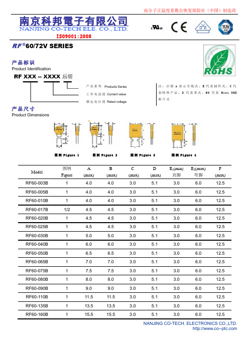
南京科邦電子有限公司NANJING CO-TECH ELE. CO., L TD.ISO9001:2008RF ®60/72V SERIES产品标识Product Identification产品系列Products Series 注:后缀A表示引线式;B代表插件式;C代表特种产品;D代表带式;M S代表M in i S MD贴片式工作电流值Current value额定电压值Rated voltage产品尺寸Product Dimensions图例F i g u r e 1图例F i g u r e 2图例F i g u r e 3图例F i g u r e 4Model图例Figure (max) (max) (max) (max)1直脚2弯脚(max) RF60-003B 1 4.0 4.0 3.0 5.1 3.0 6.0 12.5RF60-005B 1 4.0 4.0 3.0 5.1 3.0 6.0 12.5RF60-010B 1 4.0 4.0 3.0 5.1 3.0 6.0 12.5RF60-017B 1/2 4.5 4.5 3.0 5.1 3.0 6.0 12.5RF60-020B 1 4.5 4.5 3.0 5.1 3.0 6.0 12.5RF60-025B 1 4.5 4.5 3.0 5.1 3.0 6.0 12.5RF60-030B 1 5.0 5.0 3.0 5.1 3.0 6.0 12.5RF60-040B 1 6.0 6.0 3.0 5.1 3.0 6.0 12.5RF60-050B 1 6.5 6.5 3.0 5.1 3.0 6.0 12.5RF60-065B 1 7.0 7.0 3.0 5.1 3.0 6.0 12.5RF60-075B 1 7.5 7.5 3.0 5.1 3.0 6.0 12.5RF60-080B 1 8.0 8.0 3.0 5.1 3.0 6.0 12.5RF60-090B 1 9.0 9.0 3.0 5.1 3.0 6.0 12.5RF60-110B 1 11.5 11.5 3.0 5.1 3.0 6.0 12.5RF60-135B 1 13.5 13.5 3.0 5.1 3.0 6.0 12.5RF60-160B 115.5 15.5 3.0 5.1 3.0 6.0 12.5RF60-185B 1 17.5 17.5 3.0 5.1 3.0 6.0 12.5 RF60-200B 1/2 17.5 17.5 3.0 5.1/10.2 3.0 6.0 12.5 RF60-250B 2 20.0 20.0 3.0 10.2 3.0 6.0 12.5 RF60-300B 2 24.5 24.5 3.0 10.2 3.0 6.0 12.5 RF60-375B 2 24.5 24.5 3.0 10.2 3.0 6.0 12.5产品电气参数Product Electrical CharacteristicsModel I H( A )I T( A )V max( V )I max( A)Time-to-trip P(d)R.minR.maxI trip (A) T. max ( W ) (Ω)(Ω)RF60-003B 资料下载0.03 0.06 72 30 0.15 4.58s 0.24 15.0 45.0 RF60-005B 资料下载0.05 0.10 72 30 0.25 4.53s 0.26 7.30 11.10 RF60-010B 资料下载0.10 0.20 72 40 0.50 4.41s 0.38 2.50 6.50 RF60-017B 资料下载0.17 0.34 72 40 0.85 4.34s 0.40 3.30 5.21 RF60-020B 资料下载0.20 0.40 72 40 1.0 4.26s 0.41 1.83 2.84 RF60-025B 资料下载0.25 0.50 72 40 1.25 4.15s 0.45 1.25 1.95 RF60-030B 资料下载0.30 0.60 72 40 1.50 4.03s 0.49 0.80 1.56 RF60-040B 资料下载0.40 0.80 72 40 2.0 3.55s 0.56 0.55 0.86 RF60-050B 资料下载0.50 1.0 72 40 2.50 3.49s 0.77 0.50 0.77 RF60-065B 资料下载0.65 1.30 72 40 3.25 3.42s 0.88 0.20 0.65 RF60-075B 资料下载0.75 1.50 72 40 3.75 3.34s 0.92 0.25 0.40 RF60-080B 资料下载0.80 1.60 72 40 4.0 3.30s 0.95 0.15 0.30 RF60-090B 资料下载0.90 1.80 72 40 4.50 3.30s 0.99 0.20 0.30 RF60-110B 资料下载 1.10 2.20 72 40 5.50 3.26s 1.50 0.15 0.25 RF60-135B 资料下载 1.35 2.70 72 40 6.75 3.22s 1.70 0.12 0.19 RF60-160B 资料下载 1.60 3.20 72 40 8.0 3.15s 1.90 0.09 0.14 RF60-185B 资料下载 1.85 3.70 72 40 9.25 3.07s 2.10 0.08 0.19 RF60-200B 资料下载 2.0 4.0 72 40 10.0 3.02s 2.30 0.09 0.20 RF60-250B 资料下载 2.50 5.0 72 40 12.50 3.04s 2.50 0.05 0.08 RF60-300B 资料下载 3.0 6.0 72 40 15.0 2.55s 2.80 0.04 0.06 RF60-375B 资料下载 3.75 7.50 72 40 18.75 2.53s 3.20 0.03 0.05 注解Comment:IH:Hold current-maximum current at which the device will not trip at 25℃Pdmax: Power dissipated from device when in the tripped state in 25℃ still air It: Trip current-minimum current at which the device will always trip at 25℃R max: Maximum device resistance at 25℃ prior to tripping Vmax: Maximum voltage device can withstand without damage at rated R min: Minimum device resistance at 25℃ prior to tripping Imax: Maximum fault current device can withstand without damage at rated Time-to-trip: Over loading current & time产品特性曲线图Product Rate Temperature & I t r i p注:环境温度为25℃±2℃工作电流值与环境温度折减表Product Rate Temperature & I t r i pModel -20℃0℃20℃30℃40℃50℃60℃70℃85℃RF60-003B 0.041 0.036 0.030 0.027 0.024 0.022 0.019 0.016 0.014RF60-005B 0.068 0.060 0.050 0.045 0.041 0.036 0.032 0.027 0.024RF60-010B 0.136 0.119 0.100 0.090 0.081 0.072 0.063 0.054 0.047RF60-017B 0.231 0.202 0.170 0.153 0.138 0.122 0.107 0.092 0.080RF60-020B 0.272 0.238 0.200 0.180 0.162 0.144 0.126 0.108 0.094RF60-025B 0.340 0.298 0.250 0.225 0.203 0.180 0.158 0.135 0.118RF60-030B 0.408 0.357 0.300 0.270 0.243 0.216 0.189 0.162 0.141RF60-040B 0.544 0.476 0.400 0.360 0.324 0.288 0.252 0.216 0.188RF60-050B 0.680 0.595 0.500 0.450 0.405 0.360 0.315 0.270 0.235 RF60-065B 0.884 0.774 0.650 0.585 0.527 0.468 0.410 0.351 0.306 RF60-075B 1.020 0.893 0.750 0.675 0.608 0.540 0.473 0.405 0.353 RF60-080B 1.09 0.95 0.80 0.72 0.65 0.58 0.51 0.44 0.35 RF60-090B 1.224 1.071 0.900 0.810 0.729 0.648 0.567 0.486 0.423 RF60-110B 1.496 1.309 1.100 0.990 0.891 0.792 0.693 0.594 0.517 RF60-135B 1.836 1.607 1.350 1.215 1.094 0.972 0.851 0.729 0.635 RF60-160B 2.176 1.904 1.600 1.440 1.296 1.152 1.008 0.864 0.752 RF60-185B 2.516 2.202 1.850 1.665 1.499 1.332 1.166 0.999 0.870 RF60-200B 2.720 2.420 2.0 1.800 1.621 1.440 1.261 1.080 0.941 RF60-250B 3.400 2.975 2.500 2.250 2.025 1.800 1.575 1.350 1.175 RF60-300B 4.080 3.570 3.000 2.700 2.430 2.160 1.890 1.620 1.410 RF60-375B 5.100 4.463 3.750 3.375 3.038 2.700 2.363 2.025 1.763产品出厂包装Product Packing Specifications。
- 1、下载文档前请自行甄别文档内容的完整性,平台不提供额外的编辑、内容补充、找答案等附加服务。
- 2、"仅部分预览"的文档,不可在线预览部分如存在完整性等问题,可反馈申请退款(可完整预览的文档不适用该条件!)。
- 3、如文档侵犯您的权益,请联系客服反馈,我们会尽快为您处理(人工客服工作时间:9:00-18:30)。
10
谢谢!
11
7
RF60结构体系
LCOSC LPOSC
内嵌3.9GHz的LC振荡器,为FSK/ASK提供27MHz~960MHz载波频率。 在0℃~+70 ℃工作环境温度范围内,出厂校正精度±150ppm。 在-40 ℃~+85 ℃工作环境温度范围内,出厂校正精度±250ppm。 24MHz RC振荡器,为8051内核提供工作时钟。 可降低到187.5KHz以便降低功耗。 低功耗低频振荡器,振荡频率2.1KHz,为8051内核提供定时唤醒用途。 维持低频振荡仅需700nA,最大支持周期6800秒长时间唤醒(1.89小时)。 在需要高精度或工作在工业级范围情况下,可以外接10~13MHz晶体振荡器。
HopeRF新品推介——RF60
2010年8月29日
1
主要内容
1 2 3
RF60概述
RF60结构体系
结束语
2
1. 2. 3. 4.
RF60概述
SoC设计集成无线发射和8051内核于一体 主要特色
高集成度的SoC设计,无须外挂任何晶体振荡器即可工作 可实现27MHz~960MHz任意射频工作频点 最低功耗待机模式电流仅为10nA 使用差分环状PCB天线,外围射频电路非常简洁, 芯片内置天线自动匹配
±150 ±250 0.3 FSK, ASK Up to 100 up to 20 +10 19.5 0.25
MHz
ppm ppm ppm kbps kbps dBm dB dB
GPIO (按键唤醒)
6
4 (MSOP) / 8 (SOIC)
-
系统指标
RF60结构体系
射频指标
工作电压 1.8V ~ 3.6V 工作温度 -40℃ ~ +85℃(工业级) 内嵌LC振荡器(LCOSC),精度± 250ppm 封装: MOSP-10Pin (3mm× 3mm,Layout面积3mm× 6mm) SOIC-14Pin
测试条件
参数值
1.8 to 3.6 14.7 12.0 19.8 14.4 < 10
单位
V mA mA mA mA nA
射频频率
频率精度(内部LC) 频噪 (rms) 调制方式 通讯速率 最大发射功率 发射功率范围 发射功率步进 FSK ASK 0 to 70C -40 to 85C
27 to 960
应用示例(带晶体振荡器——适用常温范围ASK/FSK调制射频应用)
5
RF60概述
参数名称
工作电压范围 Tx @ +10 dBm, ASK 工作电流 (工作电压 ≥ 2.2V 输出功率 +10dBm) Tx @ +6.5 dBm, ASK Tx @ +10 dBm, FSK Tx @ +6.5 dBm, FSK 待机 @ T=25C
Sleep Timer
外接晶体振荡器
8
RF60结构体系
可编程PA 自动调节匹配天线
最大发射输出达+10dBm,发射功率范围19.5dB,调节步进0.25dB。 通过调节参数优化天线发射效率,反馈回路能实现自动调节的闭环效果,能保 证发射过程的稳定性。
9
结束语
我们不认为RF60是一颗MCU或是一颗单发射芯片,因为RF60 具备了这两者,这种结合已经密不可分。因此,我们更倾向于把 RF60定义为一个小型系统,这也是SoC最本质的趋向。这种化繁为 简、整合模块于一体,正是芯片技术发展所趋向的。 在目前市场中,还大量存在着声表面、高频管设计单发射系统。 这些小型系统都在面临着分立器件批次生产质量稳定性、线路面积 无法适应更小巧结构、功能单一且不能灵活、改变不同工作频段时 需要重新设计(甚至改变结构)等等问题。RF60正是因此而生, SoC设计正是为解决这些问题研发出新的产品,这种新旧产品的替 换,如同历史进程一般,一直往前永不倒退。
MCU指标
频率范围 27-960 MHz 最大发射功率+10 dBm,输出可调节 天线自动调整匹配 最大通讯速率支持100kbps 支持FSK/ASK两种调制模式
内嵌高速8051核,最高速度24MIPS 4KB-RAM 代码运行区域 8KB-NVM(OTP) 代码存储区域 12KB-ROM API函数库(集成AES-128加解密运算) 512Byte 内部RAM 4/8 GPIO带中断唤醒 低功耗低频振荡器(2.1KHz),仅需700nA 最低待机功耗,仅需10nA
目标市场及应用方向
市场 消费 领域 室内室外 楼宇安防 玩具 应用方向 照明调光系统、家电无线遥控、户外无线节点 电动车库门、电动闸门 高端无市场
无线遥控中控锁(RKE)
防盗报警系统
3
RF60概述
应用示例(带晶体振荡器——适用全温度范围高精度FSK调制射频应用)
4
RF60概述