电流源芯片XTR111
电压电流转换器芯片xtr111
0 to 36
mA
Current Limit for Output Current Nonlinearity, IOUT/ISET (2) (3)
1
Please be aware that an important notice concerning availability, standard warranty, and use in critical applications of Texas Instruments semiconductor products and disclaimers thereto appears at the end of this data sheet. All trademarks are the property of their respective owners.
2
PRODUCTION DATA information is current as of publication date. Products conform to specifications per the terms of the Texas Instruments standard warranty. Production processing does not necessarily include testing of all parameters.
±25
Continous to common and VVSP Continous to common and VVSP
–55 to +125 –65 to +150
2000
UNIT V V V V V mA
°C °C V
(1) Stresses above these ratings may cause permanent damage. Exposure to absolute maximum conditions for extended periods may degrade device reliability. These are stress ratings only, and functional operation of the device at these or any other conditions beyond those specified is not supported.
4-20mA电流环、电压电流转换芯片方案比较
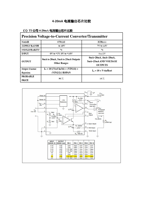
4-20mA电流输出芯片比较(1)TI公司4-20mA电流输出芯片比较Precision Voltage-to-Current Converter/Transmitter NAME XTR110 XTR111 SUPPLY RANGE to 40V7V to 44V NONLINEARITY%% INPUT0V to +5V, 0V to +10V0 to 12VOUTPUT 0mA to 20mA, 5mA to 25mA OutputsOther Ranges0mA–20mA, 4mA–20mA,5mA–25mA AND VOLTAGEOUTPUTSOutput Current Equation I O = 10 [(Vref In/16) + (VIN1/4) +(VIN2/2)] /RSPANI O = 10 × Vvin/RsetPROBABLEPRICE90元10元XTR110应用电路XTR111内部没有提供将0V输入转换成4mA输出的电路,最常用的方法是采用两个电阻网络连接参考电压和输入信号进行分压输入XTR111 应用电路4-20mA CURRENT TRANSMITTERwith Sensor Excitation and Linearization NAME XTR105XTR112XTR114 SUPPLY RANGE to 36VPRECISION CURRENT SOURCESINPUT EXCITATION2- OR 3-WIRE RTD OPERATIONOutput Current Equation IO = VIN (40/RG) + 4mA, VIN in Volts, RG in Input Offset V oltage VCM = 2VPROBABLE PRICE25元50元60元XTR105/XTR112/XTR114原理图4-20mA Current-Loop TransmitterNAME XTR115XTR116XTR117 SUPPLY RANGE to 36V to 40V VFOR SENSOR EXCITATION NC LOW QUIESCENT CURRENT200μA130A LOW SPAN ERROR%LOW NONLINEARITY ERROR%PROBABLE PRICE20元15元XTR115/XTR116/XTR117原理图RCV42——4-20mA电流转0-5V电压基本连接RCV42——4-20mA电流转0-5V电压实例XTR101--Precision, Low Drift 4-20mA TWO-WIRE TRANSMITTERXTR106-- 4-20mA CURRENT TRANSMITTER with Bridge Excitation and LinearizationXTR108-- 4-20mA, TWO-WIRE TRANSMITTER “Smart” Programmable with SignalConditioningXTR300-- Industrial Analog Current/V oltage OUTPUT DRIVER(2)AD公司4-20mA电流输出芯片比较DAC and Current TransmitterNAME AD420AD5412AD5422AD694 FUNCTION DAC4–20 mA Transmitter RESOLUTION161216-SUPPL YRANGE12-32V A VDD: A VSS:V to 36 VINPUT16BITDIGITALSerial Input12BITDIGITALSerial Input16BITDIGITALSerial InputPrecalibrated InputRanges:0 V to 2 V, 0 V to 10 VOUTPUT 4 mA to 20 mA, 0mA to 20 mA,0 mA to 24 Ma0 V to 5 V, 0 V to10 V, ±5 V, ±10 V 4 mA to 20 mA, 0mA to 20 mA,0 mA to 24 mA0 V to 5 V, 0 V to10 V, ±5 V, ±10 V4 mA to 20 mA, 0mA to 20 mA,0 mA to 24 mA0 V to 5 V, 0 V to10 V, ±5 V, ±10 V4–20 mA, 0–20 mAPROBABLEPRICE60元50元60元50元AD420—standard configurationAD5412/5422—in HART configuration AD694—standard configuration(3)AMG公司4-20mA电流输出芯片比较NAME DESCRIPTION PROBABL E PRICEAM40050元AM46040元AM46240元AM400—standard configuration AM460—standard configurationAM462—standard configuration另查过Linear和MAXIM公司无相关产品。
lm111相关资料

LM111,LM211,LM311LM111/LM211/LM311 Voltage ComparatorLiterature Number: SNOSBJ1CLM111/LM211/LM311Voltage Comparator1.0General DescriptionThe LM111,LM211and LM311are voltage comparators that have input currents nearly a thousand times lower than devices like the LM106or LM710.They are also designed to operate over a wider range of supply voltages:from standard ±15V op amp supplies down to the single 5V supply used for IC logic.Their output is compatible with RTL,DTL and TTL as well as MOS circuits.Further,they can drive lamps or relays,switching voltages up to 50V at currents as high as 50mA.Both the inputs and the outputs of the LM111,LM211or the LM311can be isolated from system ground,and the output can drive loads referred to ground,the positive supply or the negative supply.Offset balancing and strobe capability are provided and outputs can be wire OR’ed.Although slower than the LM106and LM710(200ns response time vs 40ns)the devices are also much less prone to spurious oscilla-tions.The LM111has the same pin configuration as the LM106and LM710.The LM211is identical to the LM111,except that its perfor-mance is specified over a −25˚C to +85˚C temperature range instead of −55˚C to +125˚C.The LM311has a temperature range of 0˚C to +70˚C.2.0Featuresn Operates from single 5V supplyn Input current:150nA max.over temperature n Offset current:20nA max.over temperature n Differential input voltage range:±30V nPower consumption:135mW at ±15V3.0Typical Applications(Note 3)Offset BalancingStrobing0057043600570437Note:Do Not Ground Strobe Pin.Output is turned off when current is pulled from Strobe Pin.Increasing Input Stage Current (Note 1)Detector for Magnetic Transducer00570438Note 1:Increases typical common mode slew from 7.0V/µs to 18V/µs.00570439January 2001LM111/LM211/LM311Voltage Comparator©2004National Semiconductor Corporation 3.0Typical Applications(Note 3)(Continued)Digital Transmission IsolatorRelay Driver with Strobe0057044000570441*Absorbs inductive kickback of relay and protects IC from severe voltage transients on V ++line.Note:Do Not Ground Strobe Pin.Strobing off Both Input and Output Stages (Note 2)00570442Note:Do Not Ground Strobe Pin.Note 2:Typical input current is 50pA with inputs strobed off.Note 3:Pin connections shown on schematic diagram and typical applications are for H08metal can package.Positive Peak Detector Zero Crossing Detector Driving MOS Logic00570423*Solid tantalum00570424L M 111/L M 211/L M 311 24.0Absolute Maximum Ratings for the LM111/LM211(Note10)If Military/Aerospace specified devices are required, please contact the National Semiconductor Sales Office/ Distributors for availability and specifications.Total Supply Voltage(V84)36V Output to Negative Supply Voltage(V74)50V Ground to Negative Supply Voltage(V14)30V Differential Input Voltage±30V Input Voltage(Note4)±15V Output Short Circuit Duration10sec Operating Temperature RangeLM111−55˚C to125˚C LM211−25˚C to85˚C Lead Temperature(Soldering,10sec)260˚C Voltage at Strobe Pin V+−5V Soldering InformationDual-In-Line PackageSoldering(10seconds)260˚C Small Outline PackageVapor Phase(60seconds)215˚C Infrared(15seconds)220˚C See AN-450“Surface Mounting Methods and Their Effect on Product Reliability”for other methods of soldering surface mount devices.ESD Rating(Note11)300VElectrical Characteristics(Note6)for the LM111and LM211Parameter Conditions Min Typ Max UnitsInput Offset Voltage(Note7)T A=25˚C,R S≤50k0.7 3.0mVInput Offset Current T A=25˚C 4.010nAInput Bias Current T A=25˚C60100nAVoltage Gain T A=25˚C40200V/mV Response Time(Note8)T A=25˚C200ns Saturation Voltage V IN≤−5mV,I OUT=50mA0.75 1.5VT A=25˚CStrobe ON Current(Note9)T A=25˚C 2.0 5.0mAOutput Leakage Current V IN≥5mV,V OUT=35V0.210nAT A=25˚C,I STROBE=3mAInput Offset Voltage(Note7)R S≤50k 4.0mVInput Offset Current(Note7)20nAInput Bias Current150nAInput Voltage Range V+=15V,V−=−15V,Pin7−14.513.8,-14.713.0VPull-Up May Go To5VSaturation Voltage V+≥4.5V,V−=00.230.4VV IN≤−6mV,I OUT≤8mAOutput Leakage Current V IN≥5mV,V OUT=35V0.10.5µAPositive Supply Current T A=25˚C 5.1 6.0mANegative Supply Current T A=25˚C 4.1 5.0mA Note4:This rating applies for±15supplies.The positive input voltage limit is30V above the negative supply.The negative input voltage limit is equal to the negative supply voltage or30V below the positive supply,whichever is less.Note5:The maximum junction temperature of the LM111is150˚C,while that of the LM211is110˚C.For operating at elevated temperatures,devices in the H08 package must be derated based on a thermal resistance of165˚C/W,junction to ambient,or20˚C/W,junction to case.The thermal resistance of the dual-in-line package is110˚C/W,junction to ambient.Note6:These specifications apply for V S=±15V and Ground pin at ground,and−55˚C≤T A≤+125˚C,unless otherwise stated.With the LM211,however,all temperature specifications are limited to−25˚C≤T A≤+85˚C.The offset voltage,offset current and bias current specifications apply for any supply voltage from a single 5V supply up to±15V supplies.Note7:The offset voltages and offset currents given are the maximum values required to drive the output within a volt of either supply with a1mA load.Thus,these parameters define an error band and take into account the worst-case effects of voltage gain and R S.Note8:The response time specified(see definitions)is for a100mV input step with5mV overdrive.Note9:This specification gives the range of current which must be drawn from the strobe pin to ensure the output is properly disabled.Do not short the strobe pin to ground;it should be current driven at3to5mA.Note10:Refer to RETS111X for the LM111H,LM111J and LM111J-8military specifications.Note11:Human body model,1.5kΩin series with100pF.LM111/LM211/LM31135.0Absolute Maximum Ratings for the LM311(Note 12)If Military/Aerospace specified devices are required,please contact the National Semiconductor Sales Office/Distributors for availability and specifications.Total Supply Voltage (V 84)36V Output to Negative Supply Voltage (V 74)40V Ground to Negative Supply Voltage (V 14)30VDifferential Input Voltage ±30V Input Voltage (Note 13)±15VPower Dissipation (Note 14)500mW ESD Rating (Note 19)300VOutput Short Circuit Duration 10sec Operating Temperature Range 0˚to 70˚C Storage Temperature Range−65˚C to 150˚CLead Temperature (soldering,10sec)260˚C Voltage at Strobe Pin V +−5VSoldering Information Dual-In-Line Package Soldering (10seconds)260˚C Small Outline Package Vapor Phase (60seconds)215˚C Infrared (15seconds)220˚CSee AN-450“Surface Mounting Methods and Their Effect on Product Reliability”for other methods of soldering surface mount devices.Electrical Characteristics(Note 15)for the LM311ParameterConditionsMinTyp Max Units Input Offset Voltage (Note 16)T A =25˚C,R S ≤50k 2.07.5mV Input Offset Current(Note 16)T A =25˚C 6.050nA Input Bias Current T A =25˚C 100250nA Voltage GainT A =25˚C 40200V/mV Response Time (Note 17)T A =25˚C200ns Saturation VoltageV IN ≤−10mV,I OUT =50mA 0.75 1.5V T A =25˚C Strobe ON Current (Note 18)T A =25˚C2.0 5.0mA Output Leakage CurrentV IN ≥10mV,V OUT =35V T A =25˚C,I STROBE =3mA 0.250nA V −=Pin 1=−5VInput Offset Voltage (Note 16)R S ≤50K10mV Input Offset Current (Note 16)70nA Input Bias Current 300nA Input Voltage Range −14.513.8,−14.713.0V Saturation Voltage V +≥4.5V,V −=00.230.4V V IN ≤−10mV,I OUT ≤8mA Positive Supply Current T A =25˚C 5.17.5mA Negative Supply CurrentT A =25˚C4.15.0mANote 12:“Absolute Maximum Ratings indicate limits beyond which damage to the device may occur.Operating Ratings indicate conditions for which the device is functional,but do not guarantee specific performance limits.”Note 13:This rating applies for ±15V supplies.The positive input voltage limit is 30V above the negative supply.The negative input voltage limit is equal to the negative supply voltage or 30V below the positive supply,whichever is less.Note 14:The maximum junction temperature of the LM311is 110˚C.For operating at elevated temperature,devices in the H08package must be derated based on a thermal resistance of 165˚C/W,junction to ambient,or 20˚C/W,junction to case.The thermal resistance of the dual-in-line package is 100˚C/W,junction to ambient.Note 15:These specifications apply for V S =±15V and Pin 1at ground,and 0˚C <T A <+70˚C,unless otherwise specified.The offset voltage,offset current and bias current specifications apply for any supply voltage from a single 5V supply up to ±15V supplies.Note 16:The offset voltages and offset currents given are the maximum values required to drive the output within a volt of either supply with 1mA load.Thus,these parameters define an error band and take into account the worst-case effects of voltage gain and R S .Note 17:The response time specified (see definitions)is for a 100mV input step with 5mV overdrive.Note 18:This specification gives the range of current which must be drawn from the strobe pin to ensure the output is properly disabled.Do not short the strobe pin to ground;it should be current driven at 3to 5mA.Note 19:Human body model,1.5k Ωin series with 100pF.L M 111/L M 211/L M 311 46.0LM111/LM211Typical Performance CharacteristicsInput Bias CurrentInput Bias Current0057044300570444Input Bias Current Input Bias Current0057044500570446Input Bias Current Input Bias Current0057044700570448LM111/LM211/LM31156.0LM111/LM211Typical Performance Characteristics(Continued)Input Bias Current Input OverdrivesInput Bias Current Input Overdrives0057044900570450Input Bias CurrentResponse Time for VariousInput Overdrives0057045100570452Response Time for VariousInput OverdrivesOutput Limiting Characteristics0057045300570454L M 111/L M 211/L M 311 66.0LM111/LM211Typical Performance Characteristics(Continued)Supply CurrentSupply Current0057045500570456Leakage Currents005704577.0LM311Typical Performance CharacteristicsInput Bias CurrentInput Offset Current0057045800570459LM111/LM211/LM31177.0LM311Typical Performance Characteristics(Continued)Offset ErrorInput Characteristics0057046000570461Common Mode Limits Transfer Function0057046200570463Response Time for VariousInput Overdrives Response Time for VariousInput Overdrives0057046400570465L M 111/L M 211/L M 311 87.0LM311Typical Performance Characteristics(Continued)Output Saturation VoltageResponse Time for VariousInput Overdrives0057046600570467Response Time for VariousInput OverdrivesOutput Limiting Characteristics0057046800570469Supply Current Supply Current0057047000570471LM111/LM211/LM31197.0LM311Typical Performance Characteristics(Continued)Leakage Currents005704728.0Application Hints8.1CIRCUIT TECHNIQUES FOR AVOIDINGOSCILLATIONS IN COMPARATOR APPLICATIONSWhen a high-speed comparator such as the LM111is used with fast input signals and low source impedances,the out-put response will normally be fast and stable,assuming that the power supplies have been bypassed (with 0.1µF disc capacitors),and that the output signal is routed well away from the inputs (pins 2and 3)and also away from pins 5and 6.However,when the input signal is a voltage ramp or a slow sine wave,or if the signal source impedance is high (1k Ωto 100k Ω),the comparator may burst into oscillation near the crossing-point.This is due to the high gain and wide band-width of comparators like the LM111.To avoid oscillation or instability in such a usage,several precautions are recom-mended,as shown in Figure 1below.1.The trim pins (pins 5and 6)act as unwanted auxiliaryinputs.If these pins are not connected to a trim-pot,they should be shorted together.If they are connected to a trim-pot,a 0.01µF capacitor C1between pins 5and 6will minimize the susceptibility to AC coupling.A smaller capacitor is used if pin 5is used for positive feedback as in Figure 1.2.Certain sources will produce a cleaner comparator out-put waveform if a 100pF to 1000pF capacitor C2is connected directly across the input pins.3.When the signal source is applied through a resistivenetwork,R S ,it is usually advantageous to choose an R S 'of substantially the same value,both for DC and for dynamic (AC)considerations.Carbon,tin-oxide,and metal-film resistors have all been used successfully in comparator input circuitry.Inductive wirewound resistors are not suitable.4.When comparator circuits use input resistors (eg.sum-ming resistors),their value and placement are particu-larly important.In all cases the body of the resistor should be close to the device or socket.In other words there should be very little lead length or printed-circuit foil run between comparator and resistor to radiate or pick up signals.The same applies to capacitors,pots,etc.For example,if R S =10k Ω,as little as 5inches oflead between the resistors and the input pins can result in oscillations that are very hard to damp.Twisting these input leads tightly is the only (second best)alternative to placing resistors close to the comparator.5.Since feedback to almost any pin of a comparator canresult in oscillation,the printed-circuit layout should be engineered thoughtfully.Preferably there should be a groundplane under the LM111circuitry,for example,one side of a double-layer circuit card.Ground foil (or,posi-tive supply or negative supply foil)should extend be-tween the output and the inputs,to act as a guard.The foil connections for the inputs should be as small and compact as possible,and should be essentially sur-rounded by ground foil on all sides,to guard against capacitive coupling from any high-level signals (such as the output).If pins 5and 6are not used,they should be shorted together.If they are connected to a trim-pot,the trim-pot should be located,at most,a few inches away from the LM111,and the 0.01µF capacitor should be installed.If this capacitor cannot be used,a shielding printed-circuit foil may be advisable between pins 6and 7.The power supply bypass capacitors should be lo-cated within a couple inches of the LM111.(Some other comparators require the power-supply bypass to be lo-cated immediately adjacent to the comparator.)6.It is a standard procedure to use hysteresis (positivefeedback)around a comparator,to prevent oscillation,and to avoid excessive noise on the output because the comparator is a good amplifier for its own noise.In the circuit of Figure 2,the feedback from the output to the positive input will cause about 3mV of hysteresis.How-ever,if R S is larger than 100Ω,such as 50k Ω,it would not be reasonable to simply increase the value of the positive feedback resistor above 510k Ω.The circuit of Figure 3could be used,but it is rather awkward.See the notes in paragraph 7below.L M 111/L M 211/L M 3118.0Application Hints(Continued)7.When both inputs of the LM111are connected to activesignals,or if a high-impedance signal is driving the positive input of the LM111so that positive feedback would be disruptive,the circuit of Figure1is ideal.The positive feedback is to pin5(one of the offset adjust-ment pins).It is sufficient to cause1to2mV hysteresis and sharp transitions with input triangle waves from a few Hz to hundreds of kHz.The positive-feedback signal across the82Ωresistor swings240mV below the posi-tive supply.This signal is centered around the nominal voltage at pin5,so this feedback does not add to the V OS of the comparator.As much as8mV of V OS can be trimmed out,using the5kΩpot and3kΩresistor as shown.8.These application notes apply specifically to the LM111,LM211,LM311,and LF111families of comparators,and are applicable to all high-speed comparators in general, (with the exception that not all comparators have trim pins).00570429Pin connections shown are for LM111H in the H08hermetic packageFIGURE1.Improved Positive Feedback00570430 Pin connections shown are for LM111H in the H08hermetic packageFIGURE2.Conventional Positive Feedback LM111/LM211/LM3118.0Application Hints(Continued)9.0Typical Applications(Pin numbersrefer to H08package)Zero Crossing Detector Driving MOS Switch 100kHz Free Running Multivibrator0057041300570414*TTL or DTL fanout of two00570431FIGURE 3.Positive Feedback with High Source ResistanceL M 111/L M 211/L M 3119.0Typical Applications (Pin numbers refer to H08package)(Continued)10Hz to 10kHz Voltage Controlled Oscillator00570415*Adjust for symmetrical square wave time when V IN =5mV †Minimum capacitance 20pF Maximum frequency 50kHzDriving Ground-Referred Load Using Clamp Diodes to Improve Response00570416*Input polarity is reversed when using pin 1as output.00570417TTL Interface with High Level Logic00570418*Values shown are for a 0to 30V logic swing and a 15V threshold.†May be added to control speed and reduce susceptibility to noise spikes.LM111/LM211/LM3119.0Typical Applications (Pin numbers refer to H08package)(Continued)Crystal OscillatorComparator and Solenoid Driver0057041900570420Precision Squarer00570421*Solid tantalum†Adjust to set clamp levelL M 111/L M 211/L M 3119.0Typical Applications (Pin numbers refer to H08package)(Continued)Low Voltage Adjustable Reference Supply00570422*Solid tantalumPositive Peak Detector Zero Crossing Detector Driving MOS Logic00570423*Solid tantalum00570424Negative Peak Detector00570425*Solid tantalumLM111/LM211/LM3119.0Typical Applications (Pin numbers refer to H08package)(Continued)Precision Photodiode Comparator00570426*R2sets the comparison level.At comparison,the photodiode has less than 5mV across it,decreasing leakages by an order of magnitude.Switching Power Amplifier00570427L M 111/L M 211/L M 3119.0Typical Applications(Pin numbers refer to H08package)(Continued)Switching Power Amplifier00570428LM111/LM211/LM31110.0Schematic Diagram(Note 20)00570405Note 20:Pin connections shown on schematic diagram are for H08package.L M 111/L M 211/L M 31111.0Connection DiagramsMetal Can Package00570406Note:Pin 4connected to caseTop ViewOrder Number LM111H,LM111H/883(Note 21),LM211H or LM311HSee NS Package Number H08CDual-In-Line PackageDual-In-Line Package00570434Top ViewOrder Number LM111J-8,LM111J-8/883(Note 21),LM311M,LM311MX or LM311NSee NS Package Number J08A,M08A or N08E00570435Top ViewOrder Number LM111J/883(Note 21)See NS Package Number J14A or N14A00570433Order Number LM111W/883(Note 21),LM111WG/883See NS Package Number W10A,WG10ANote 21:Also available per JM38510/10304LM111/LM211/LM31112.0Physical Dimensionsinches (millimeters)unless otherwise notedMetal Can Package (H)Order Number LM111H,LM111H/883,LM211H or LM311HNS Package Number H08CCavity Dual-In-Line Package (J)Order Number LM111J-8,LM111J-8/883NS Package Number J08AL M 111/L M 211/L M 311 2012.0Physical Dimensionsinches (millimeters)unless otherwise noted (Continued)Dual-In-Line Package (J)Order Number LM111J/883NS Package Number J14ADual-In-Line Package (M)Order Number LM311M,LM311MXNS Package Number M08ALM111/LM211/LM3112112.0Physical Dimensionsinches (millimeters)unless otherwise noted (Continued)Dual-In-Line Package (N)Order Number LM311N NS Package Number N08EOrder Number LM111W/883,LM111WG/883NS Package Number W10A,WG10AL M 111/L M 211/L M 311 22NotesNational does not assume any responsibility for use of any circuitry described,no circuit patent licenses are implied and National reserves the right at any time without notice to change said circuitry and specifications.For the most current product information visit us at .LIFE SUPPORT POLICYNATIONAL’S PRODUCTS ARE NOT AUTHORIZED FOR USE AS CRITICAL COMPONENTS IN LIFE SUPPORT DEVICES OR SYSTEMS WITHOUT THE EXPRESS WRITTEN APPROVAL OF THE PRESIDENT AND GENERAL COUNSEL OF NATIONAL SEMICONDUCTOR CORPORATION.As used herein:1.Life support devices or systems are devices or systemswhich,(a)are intended for surgical implant into the body,or(b)support or sustain life,and whose failure to perform whenproperly used in accordance with instructions for use provided in the labeling,can be reasonably expected to result in a significant injury to the user.2.A critical component is any component of a life supportdevice or system whose failure to perform can be reasonably expected to cause the failure of the life support device or system,or to affect its safety or effectiveness.BANNED SUBSTANCE COMPLIANCENational Semiconductor certifies that the products and packing materials meet the provisions of the Customer Products Stewardship Specification(CSP-9-111C2)and the Banned Substances and Materials of Interest Specification(CSP-9-111S2)and contain no‘‘Banned Substances’’as defined in CSP-9-111S2.National Semiconductor Americas CustomerSupport CenterEmail:new.feedback@ Tel:1-800-272-9959National SemiconductorEurope Customer Support CenterFax:+49(0)180-5308586Email:europe.support@Deutsch Tel:+49(0)6995086208English Tel:+44(0)8702402171Français Tel:+33(0)141918790National SemiconductorAsia Pacific CustomerSupport CenterEmail:ap.support@National SemiconductorJapan Customer Support CenterFax:81-3-5639-7507Email:jpn.feedback@Tel:81-3-5639-7560 LM111/LM211/LM311 Voltage ComparatorIMPORTANT NOTICETexas Instruments Incorporated and its subsidiaries(TI)reserve the right to make corrections,modifications,enhancements,improvements, and other changes to its products and services at any time and to discontinue any product or service without notice.Customers should obtain the latest relevant information before placing orders and should verify that such information is current and complete.All products are sold subject to TI’s terms and conditions of sale supplied at the time of order acknowledgment.TI warrants performance of its hardware products to the specifications applicable at the time of sale in accordance with TI’s standard warranty.Testing and other quality control techniques are used to the extent TI deems necessary to support this warranty.Except where mandated by government requirements,testing of all parameters of each product is not necessarily performed.TI assumes no liability for applications assistance or customer product design.Customers are responsible for their products and applications using TI components.To minimize the risks associated with customer products and applications,customers should provide adequate design and operating safeguards.TI does not warrant or represent that any license,either express or implied,is granted under any TI patent right,copyright,mask work right, or other TI intellectual property right relating to any combination,machine,or process in which TI products or services are rmation published by TI regarding third-party products or services does not constitute a license from TI to use such products or services or a warranty or endorsement e of such information may require a license from a third party under the patents or other intellectual property of the third party,or a license from TI under the patents or other intellectual property of TI.Reproduction of TI information in TI data books or data sheets is permissible only if reproduction is without alteration and is accompanied by all associated warranties,conditions,limitations,and notices.Reproduction of this information with alteration is an unfair and deceptive business practice.TI is not responsible or liable for such altered rmation of third parties may be subject to additional restrictions.Resale of TI products or services with statements different from or beyond the parameters stated by TI for that product or service voids all express and any implied warranties for the associated TI product or service and is an unfair and deceptive business practice.TI is not responsible or liable for any such statements.TI products are not authorized for use in safety-critical applications(such as life support)where a failure of the TI product would reasonably be expected to cause severe personal injury or death,unless officers of the parties have executed an agreement specifically governing such use.Buyers represent that they have all necessary expertise in the safety and regulatory ramifications of their applications,and acknowledge and agree that they are solely responsible for all legal,regulatory and safety-related requirements concerning their products and any use of TI products in such safety-critical applications,notwithstanding any applications-related information or support that may be provided by TI.Further,Buyers must fully indemnify TI and its representatives against any damages arising out of the use of TI products in such safety-critical applications.TI products are neither designed nor intended for use in military/aerospace applications or environments unless the TI products are specifically designated by TI as military-grade or"enhanced plastic."Only products designated by TI as military-grade meet military specifications.Buyers acknowledge and agree that any such use of TI products which TI has not designated as military-grade is solely at the Buyer's risk,and that they are solely responsible for compliance with all legal and regulatory requirements in connection with such use. TI products are neither designed nor intended for use in automotive applications or environments unless the specific TI products are designated by TI as compliant with ISO/TS16949requirements.Buyers acknowledge and agree that,if they use any non-designated products in automotive applications,TI will not be responsible for any failure to meet such requirements.Following are URLs where you can obtain information on other Texas Instruments products and application solutions:Products ApplicationsAudio /audio Communications and Telecom /communicationsAmplifiers Computers and Peripherals /computersData Converters Consumer Electronics /consumer-appsDLP®Products Energy and Lighting /energyDSP Industrial /industrialClocks and Timers /clocks Medical /medicalInterface Security /securityLogic Space,Avionics and Defense /space-avionics-defense Power Mgmt Transportation and Automotive /automotiveMicrocontrollers Video and Imaging /videoRFID OMAP Mobile Processors /omapWireless Connectivity /wirelessconnectivityTI E2E Community Home Page Mailing Address:Texas Instruments,Post Office Box655303,Dallas,Texas75265Copyright©2011,Texas Instruments Incorporated。
xtr111参数手册

xtr111参数手册
参数手册是关于xtr111的详细信息和使用指引的文档。
xtr111是一种特殊的设备,具有许多参数和功能供用户使用和调整。
以下是xtr111参数手册中的一些重
要内容:
1. 介绍:本节介绍了xtr111的概述,包括其作用、功能和优势。
这部分还简要
介绍了xtr111的应用领域和使用注意事项。
2. 规格:这一部分列出了xtr111的所有技术规格和性能参数。
例如输入电压范围、工作温度、输出电压精度等。
这些规格参数对于使用者来说非常重要,以便确保设备在正确的条件下正常工作。
3. 连接和接口:在本节中,将详细说明xtr111的连接和接口方面的信息。
这包
括提供电源的电缆插口、通信接口和数据传输方法。
此外,还可以提供一些示意图,以帮助用户理解如何正确连接xtr111设备。
4. 配置设置:该部分涵盖了xtr111配置的相关参数。
包括输出电压范围、故障
保护设置、输入滤波等。
此外,还提供了如何使用特定工具或接口进行配置的说明。
5. 故障排除:在这一节中,提供了一些常见问题和解决方案。
用户可以在遇到
问题时参考这些步骤,以快速定位和解决问题。
6. 附录:这一部分可能包含xtr111的额外信息,如参考资料、兼容性列表等。
用户可以在需要时查阅这些额外信息。
通过阅读xtr111参数手册,用户将能够全面了解xtr111设备以及其相关配置、连接和故障排除。
这将有助于用户正确使用和调整xtr111设备,以满足其特定的
需求。
请参考本手册以获得详细指导。
精密恒流源芯片
精密恒流源芯片精密恒流源芯片(Precision Constant Current Source Chip)是一种集成电路芯片,用于提供稳定的恒定电流输出。
它可以广泛应用于各种需要恒定电流供应的电路和系统中,如LED照明、激光驱动、电池充放电管理等领域。
一、精密恒流源芯片的原理和特点精密恒流源芯片基于负反馈原理工作,通过对输入电压进行精准调节和控制,使得输出电流始终保持恒定。
其主要特点包括以下几个方面:1. 高精度:精密恒流源芯片具有很高的电流输出精度,可实现毫安级别甚至微安级别的恒流输出,满足对电流精度要求较高的应用场景。
2. 宽输入电压范围:精密恒流源芯片能够适应不同的输入电压范围,通常可以支持从几伏到几十伏的输入电压,并能在这个范围内保持恒定的输出电流。
3. 温度稳定性好:精密恒流源芯片在不同的温度环境下,能够保持输出电流的稳定性,不受环境温度的影响。
4. 低功耗:精密恒流源芯片在工作时消耗的功率较低,能够提高系统的能效。
精密恒流源芯片具有广泛的应用前景,在许多领域都有重要的作用。
1. LED照明:精密恒流源芯片可以用于LED照明系统中,通过提供恒定的电流,确保LED的亮度和颜色的稳定性,提高照明效果和寿命。
2. 激光驱动:精密恒流源芯片可以用于激光器的驱动电路中,通过提供恒定的电流,确保激光器输出的功率和波长的稳定性。
3. 电池充放电管理:精密恒流源芯片可以用于电池充放电管理系统中,通过提供恒定的充电或放电电流,实现对电池的精确管理和保护。
4. 传感器驱动:精密恒流源芯片可以用于传感器的驱动电路中,通过提供恒定的电流,保证传感器的工作稳定性和精度。
5. 仪器仪表:精密恒流源芯片可以用于各种仪器仪表中,如电流源、电压源等,通过提供稳定的电流输出,实现对被测量对象的准确测量。
三、精密恒流源芯片的发展趋势随着科技的不断进步和需求的不断增加,精密恒流源芯片的发展也呈现出一些新的趋势。
1. 集成度提高:精密恒流源芯片的集成度将不断提高,功能更加丰富,体积更小,功耗更低,以满足对集成度要求越来越高的应用需求。
xtr111用法
xtr111用法
Xtr111是一种常用的电子元件,广泛用于各种电路和系统中。
它具有多种功能
和用途,并可以根据具体需求进行灵活配置和应用。
首先,xtr111常见的使用方式是作为电压参考源。
在许多电子设备和仪器中,
为了确保精确的电压测量和控制,需要一个稳定可靠的参考电压源。
xtr111提供了
这样一种功能,它能够提供稳定的参考电压输出,从而确保电路的精确性和可靠性。
其次,xtr111还可以用作电流传感器。
在一些需要监测和控制电流的应用中,xtr111可以连接到电流传感器,并通过测量电压来间接测量电流值。
这种使用方式
可以广泛应用于工业自动化、电力监测和电子设备中。
此外,xtr111还可以用于温度测量和控制。
通过连接温度传感器和xtr111,我
们可以实现对温度的精确测量和控制。
这对于一些需要温度稳定性和精度的应用非常重要,如医疗设备、实验室仪器和热管理系统等。
最后,xtr111还可以用于电压放大和信号处理。
它可以将输入信号放大,并进
行滤波和调节,以满足特定应用的需求。
这在许多电子系统和仪器中是非常常见的使用方式。
总之,xtr111具有广泛的用途和功能,可以在多个领域中发挥重要作用。
无论
是作为电压参考源、电流传感器、温度测量还是信号处理,xtr111都能够提供可靠
的解决方案和稳定的性能。
它的灵活性和可配置性使得它成为许多电子工程师和系统设计师的首选元件之一。
xtr105电路原理图 xtr105中文资料应用电路图 英文数据手册
1. 具有很低的调整性误差; 2. 具有两个高精度的电流镜像源,800uA 每个。 3. 具有很好的线性化,这个能满足大多数工程的应用。 4. 高电压抑制比,高共模抑制比,还有很宽的电压工作范围,这个 对电源设计者来说很方便。 5. 比较低的偏移(温度特性下)每变化 1 度误差仅为 0.4uv,这对于很 对运放的指标来说,已经很不错了。很多单运放还没这个指标。电流噪声也 很低,只有 30na,这个是峰值,平均比这个水平还要低。 从下面的图可以看出来,上面所分析的特性:
点击此处跳转到页面下载:XTR105 中文资料 点击此处跳转到页面下载:XTR105 英文数据手册 XTR105 应用电路图 XTR105 是一款单芯集成的 4-20mA 的电流源芯片.芯片本身提供了两 个高精度的电流激励源,此电流激励源可以用于铂电阻的镜像电源,或者桥 式电阻的电流源,用于测试温度或者压力。电路本身具有增益可调功能,可 以省略外部的运放,达到节省成本的目的。 XTR105 应用电路,如下图所示: XTR105 应用电路图 XTR105 的性能特点如下:
xtr105 电路原理图 xtr105 中文资料应用电路图 英文
数据手册
XTR105 电路图、原理图 XTR105 是带传感器激励和传感器信号线性化处理的 420mA 电流变 送器,它在 XTR101 的基础上增加了线性化处理及基准电压源电路。基本性 能及电参数为:二线或三线制 RTD-I 作,低温漂(0.4tLV 门 C),低噪声 (30nAp-p),高 CMRR(86dBt 最小),工作电源为 7.536V。其内部电路功能图 如下所示: XTR105 电路原理图 XTR105 特征曲线
xtr111参数手册
xtr111参数手册1. 简介XTR111是一款高精度电流和电压转换器,具有广泛的应用领域。
本参数手册将介绍XTR111的主要特性、电气参数和工作原理,以帮助用户充分了解和正确使用该设备。
2. 特性概述- 高精度:XTR111具有优秀的电流和电压测量精度,可满足各类精密测量需求。
- 宽输入电压范围:XTR111可在较大的输入电压范围内工作,适用于各种电源和信号传输环境。
- 温度补偿:XTR111内置了温度补偿电路,可自动校正温度对测量结果的影响,提高稳定性和准确度。
- 低功耗:XTR111采用低功耗设计,适合用于电池供电或需要节能的应用中。
- 通信接口:XTR111支持多种通信接口,如SPI和I2C,以便用户方便地与其他设备进行数据交互。
3. 电气参数- 输入电压范围:XTR111的输入电压范围为0V至5V,可覆盖大部分应用场景。
- 电流测量范围:XTR111可测量的电流范围为0A至20A,适用于各种电流测量需求。
- 工作温度范围:XTR111的工作温度范围为-40℃至85℃,能够适应各类工作环境。
- 输出分辨率:XTR111的输出分辨率为16位,可提供较高的数据精度和准确度。
- 供电电压:XTR111的供电电压为3.3V至5.5V,可适应不同的供电环境。
4. 工作原理XTR111利用内部放大器和增益控制电路对输入电流和电压进行放大和转换。
它使用高精度的模拟数字转换器(ADC)将模拟信号转换为数字信号,并通过通信接口将数据传输给主控设备。
同时,XTR111内置的温度传感器和温度补偿电路,能够自动校正温度对测量结果的影响,提高测量的准确性和稳定性。
5. 应用领域- 工业自动化:XTR111可用于测量和监控工业设备中的电流和电压,以实现对设备状态的实时分析和控制。
- 电力系统:XTR111可用于电力系统中的电流和电压测量,用于实现电能计量和电力负荷分析。
- 仪器仪表:XTR111的高精度和稳定性使其成为仪器仪表中常用的测量模块,广泛应用于各种精密测量设备中。
基准电流源芯片
基准电流源芯片基准电流源芯片是一种用于提供稳定、精确电流输出的集成电路芯片。
它在各种电子设备中广泛应用,如模拟电路、功率放大器、传感器、仪器仪表等领域。
基准电流源芯片通过精心设计的电路和稳定的参考电压来产生所需的恒定电流输出。
基准电流源芯片的基本原理是利用稳定的电压参考源和精密的电流源来产生所需的恒定电流。
稳定的电压参考源可以是基准电压源、温度补偿电压源等。
精密的电流源可以通过电流源镜像电路、差分放大电路等实现。
基准电流源芯片通常还具有过流保护、温度补偿、输出短路保护等功能。
基准电流源芯片的主要特点是输出电流稳定、精确度高、温度稳定性好。
它可以提供从几微安到几百毫安的恒定电流输出,满足各种应用的需求。
基准电流源芯片还具有低功耗、小尺寸、易于集成等特点,适合在各种电子设备中使用。
在模拟电路中,基准电流源芯片常用于产生偏置电流、校准电流等。
它可以保证电路的工作点稳定,提高电路的性能和可靠性。
在功率放大器中,基准电流源芯片可以用于稳定输出电流,避免功率管的过流和过热现象,提高功率放大器的效率和线性度。
在传感器中,基准电流源芯片可以提供稳定的电流供给,保证传感器的工作稳定性和灵敏度。
在仪器仪表中,基准电流源芯片可以用于校准电流表、电压表等,提高仪器的测量准确度。
基准电流源芯片的选择主要考虑以下几个方面:输出电流范围、输出精度、温度稳定性、供电电压范围、功耗等。
根据具体应用需求,选择合适的基准电流源芯片非常重要。
在选择基准电流源芯片时,还要考虑其稳定性和可靠性,以及供应商的技术支持和售后服务。
目前市场上有许多知名的基准电流源芯片供应商,如ADI、TI、NS 等。
它们提供了丰富的基准电流源芯片产品系列,满足不同应用的需求。
同时,这些供应商还提供了详细的产品手册、应用笔记、参考设计等技术支持资料,帮助工程师选型和设计。
基准电流源芯片是一种关键的集成电路芯片,广泛应用于各种电子设备中。
它通过精心设计的电路和稳定的参考电压来产生稳定、精确的恒定电流输出。
xtr111用法
xtr111用法
XTR111是一种高精度电流和电压输出传感器和放大器。
它通常用
于测量和放大微弱电信号,使其可以在测控系统中准确、可靠地处理
和分析。
XTR111的主要用途包括但不限于以下几个方面:
1.控制和监测电池充放电:XTR111可以用来监测电池组的电流和
电压,帮助监控电池充电和放电过程,从而确保电池的安全和稳定工作。
2.电流传感:XTR111可以用作电流电平测量的传感器,在车辆电
子系统中常用于测量各种电动设备的电流,例如发动机控制模块、电
动机控制系统等。
3.温度控制系统:XTR111可通过与温度传感器结合使用,实现精
准的温度测量和控制,广泛应用于空调系统、电炉、温室控制等领域。
4.仪表和自动化控制系统:XTR111可以用于测量和放大传感器信号,例如压力传感器、声音传感器等,使其能够有效地被处理和控制,从而实现仪表和自动化控制系统的可靠运行。
此外,XTR111还具有以下几个特点:
-高精度:XTR111具有高输入阻抗和低噪声,可以实现对微弱电信号的精确测量和放大。
-宽工作电压范围:XTR111可以在广泛的工作电压范围内工作,从±2.25V到±18V,适用于不同的电源供应系统。
-低功耗:XTR111采用低功耗设计,能够以最小的能量消耗进行长时间稳定工作。
总之,XTR111是一种多功能的电流和电压输出传感器和放大器,
可在多个领域中应用。
通过准确测量和放大微弱电信号,它可以为测
控系统提供可靠的数据和有效的控制,提高系统性能和稳定性。
- 1、下载文档前请自行甄别文档内容的完整性,平台不提供额外的编辑、内容补充、找答案等附加服务。
- 2、"仅部分预览"的文档,不可在线预览部分如存在完整性等问题,可反馈申请退款(可完整预览的文档不适用该条件!)。
- 3、如文档侵犯您的权益,请联系客服反馈,我们会尽快为您处理(人工客服工作时间:9:00-18:30)。
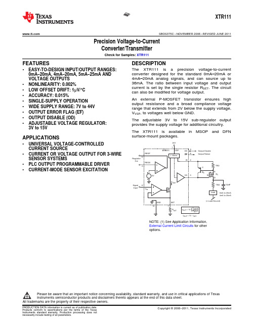
高精度电压至电流转换器XTR111
XTR111 是一款专门针对标准0mA-20mA 或4mA-20mA 模拟信号而精心设计的高精度电压至电流转换器(voltage-to-current converter),其能够提供高达36mA 的电流。
电阻器RSET 可对输入电压与输出电流之比进行设置。
此外,该产品也可针对电压输出进行调整。
外部P-MOSFET 晶体管可确保实现极高的输出阻抗以及宽泛的恒流制输出电压范围(compliance voltage),从2V 的VVSP 电压至低于GND 的电压。
可调的3V~15V 子稳压器输出能够为额外的电路系统提供电源电压。
XTR111 采用DFN 表面贴装封装。
关键特性 :
易于设计的输入/输出范围;0mA-20mA、4mA-20mA、5mA-25mA 及电压输出;
非线性度:0.002%;
低失调电压漂移:1μV/°C;
精确度:0.015%;
单电源工作;
宽泛的电压范围:7V~44V;
输出误差标记(EF);
输出禁用(OD);
稳压器可调范围:3V~15V。
应用范围:
通用的电压可控制电流源;
针对3线传感器系统的电流或电压输出;
PLC 输出可编程驱动器;
电流模式传感器激发。