2017年电子版本彩页资料
ISO TS22163-2017质量手册(含全套乌龟图)

Q/BD XXXXXX股份有限公司企业标准BD-QM-01质量手册2018-04-20 发布2018-04-03 实施XXXXX股份有限公司发布BD-QM-01质量手册版本号:3.0BD-QM-01质量手册版本号:3.0目录01.颁布令 (3)02.任命书 (4)03.公司组织架构图 (8)04.公司简介 (9)05. 经营理念 (10)06.术语和定义 (11)07.质量方针、安全方针、质量目标、安全目标、及售后服务承诺 (12)08.CRCC 产品认证的一致性要求 (14)09 附录 (15)1.附录一《任命过程所有者名单》BD‐QM‐01/01 (15)2.附录二《ISO/TS 22163 过程要素对照表》BD‐QM‐01/02 (15)3.附录三《质量管理体系过程关系流程图》BD‐QM‐01/03 (15)4.附录四《顾客导向、管理和支持过程关系图》BD‐QM‐01/04 (15)4.附录五《过程乌龟图》BD‐QM‐01/05 (15)5.附录六《KPI 绩效数据统计表》BD‐QM‐01/06 (15)6.附录《程序文件清单》BD‐QM‐01/07 (15)BD-QM-01质量手册版本号:3.001.颁布令颁布令本公司质量管理体系依据 ISO/TS 22163 技术规范(以下简称 22163)、ISO9001:2015 以及 CRCC 认证规则,结合XXXXXX股份有限公司的实际情况而建立的。
本手册是公司质量管理体系的法规性文件,通过本手册发布的公司质量方针以及体系运行的各项规定已得到本人全面认定,准予颁布实施,公司全体员工必须遵照执行。
最高管理者(总经理)签名年月日BD-QM-01质量手册版本号:3.0 02.任命书任命书(一)为确保公司质量方针的有效履行和本手册各项规定的贯彻实施,兹任命质保中心总监XXXXX为我公司质量管理体系管理者代表(简称管理者代表),协助最高管理者履行以下职责:1.确保质量管理体系所需的过程得到建立、实施和保持;2.向最高管理者报告质量体系绩效和任何改进的需求;3.确保在整个组织内提高满足顾客要求的意识;4.在组织中解决质量相关问题的自主权,或在关键要求未满足时,停止开发、生产、交付、现场支持活动的权利;5.就质量管理体系有关事宜与外部方进行联络。
电子政务外网分时隔离上网场景彩页

电子政务外网分时隔离上网场景行业建设趋势为贯彻落实《政务信息系统整合共享实施方案》(国办发[2017]39号)的建设要求,各省(市/区)积极按照“统一规划、统一网络”的要求,全面推进电子政务外网互联网出口统一以及各委办局业务系统整合。
行业应用特点各委办局的终端上网办公可能访问多个网络,需要访问互联网、政务外网的公共数据区以及业务专网区。
拓扑图业务安全常见问题1、委办局办公人员的同一台PC同时可以访问互联网、政务外网,容易形成跳板攻击,不符合国家电子政务外网的建设要求;2、委办局接入终端的身份不明晰,无法实现权限划分;3、部分委办局网络出口设置NAT转换,出现违规访问行为,无法追溯到人。
传统解决方案的问题1.使用物理隔离卡或两台物理PC,构建多套物理隔离网络a)终端改造建设投资大,实施困难;b)不符合政府部门终端复用的建设趋势要求。
2.委办局办公终端无需认证即可接入电子政务外网办公终端可随意接入政务外网,存在安全隐患,不符合国家电子政务外网有关终端接入的安全要求。
3.政府信息中心部署网络审计设备委办局进行NAT转换后,只能审计到整体的访问行为,出现安全事件后无法追溯到个人。
深信服创新解决办法1. 委办局单位公务员自注册身份账号,实名认证接入(1)公务员自注册账号,绑定手机号和部门员工访问网络前,先注册政务网账号,填写姓名、部门、密码等,绑定个人手机号;管理员审核后方可生效。
(2)终端第一次访问政务外网时,均需要进行实名认证,否则无法访问。
2. 实现政务网和互联网安全隔离访问同一时间委办人员只能访问政务外网和互联网中的一个,当接入政务外网时,会自动断开互联网的访问;且可以轻松实现多个网络的访问切换。
3.网络访问审计可追溯对委办人员访问政务外网的行为进行全面审计,方便事后追溯查询,包括政务网账号、源IP/MAC、所属单位、目的IP等。
用户可获取的收益1. 委办局的办公PC只能同时访问一个网络,实现互联网、政务外网以及业务专网的安全隔离访问;2. 实现电子政务外网接入实名认证,保障接入政务外网的终端身份合法性;3. 实现委办局办公人员的网络访问审计,根据后续需要可追溯到个人。
彩页文档完整版

卓立酒庄简介Zhuoli Wineries卓立酒庄是一家进口葡萄酒的贸易公司。
酒庄自拥2个法国自主品牌,“芙蓉·德”红葡萄酒和“白岛”白葡萄酒,均源于波尔多地区拉古缘纳酒业集团(LA GUYENNOISE)的兰萨德古堡(Château Lansade)。
拉古缘纳公司介绍LA GUYENNOISE拉古缘纳(LA GUYENNOISE)公司位于波尔多葡萄酒产区中心地域。
集团奠基人米歇尔•马丁(Michel Martin)出身酒农世家。
其父皮埃尔•马丁先生(Pierre Martin)是法国首个酒农协会-豪赞酒农合作社(the wine cooperative of Rauzan)的创建元老,并担任法国酒农合作社(the National Federation of French Wine Cooperatives)全国联盟主席长达35年。
兰萨德酒庄简介Château Lansade兰萨德古堡庄园(Château Lansade)位于两海之间产区最美的地段,覆盖了加隆河与多尔多捏河之间的宽广地域。
葡萄园面积为30公顷,各葡萄品种的分布均衡适宜。
卓立酒庄与兰萨德庄园建立长期合作伙伴关系,公司秉承“原瓶原装进口”原则,确保每瓶酒“庄园酿造,庄园灌装”。
“芙蓉·德”系列干红葡萄酒Fleur de Lansade1.托洛桑伯爵红葡萄酒Comte Tolosan原产地:法国Origin:France葡萄品种:40%品丽珠,30%梅洛,30%嘉美Grape varieties: 40%Carbernet franc, 30%Merlot, 30%Gamay等级:地区餐酒(IGP)Rank: IGP侍酒温度:16-18℃Serve at:16-18℃品酒记录:观色:酒体呈浅宝石红色闻香:樱桃,果酱的红色水果香气突出品味:微甜口感带有中等酸度,丹宁中等偏低,酒体轻盈和谐。
2017年秋季学期新人教版四年级语文上册全一册高效课堂导学案
小学语文第七册高效课堂导学案班级课题 1观潮课时 2课时使用时间组别姓名小组评价教师评价编制李秋燕审核小学语文第七册高效课堂导学案班级课题2* 雅鲁藏布大峡谷课时 1课时使用日期小学语文第七册高效课堂导学案班级课题 3 鸟的天堂课时 2课时使用日期小学语文第七册高效课堂导学案班级课题 4* 火烧云课时 1课时使用时间组别姓名小组评价教师评价编制任明容审核小学语文第七册高效课堂导学案班级课题 5古诗两首课时 2课时使用时间组别姓名小组评价教师评价编制任明容审核小学语文第七册高效课堂导学案班级课题 6、爬山虎的脚课时 2课时使用时间组别姓名小组评价教师评价编制任明容审核小学语文第七册高效课堂导学案班级课题7蟋蟀的住宅课时 2课时使用日期组别使用人小组评价:教师评价:主备人马德莉审核人小学语文第七册高效课堂导学案班级课题8﹡世界地图引出的发现课时 1课时使用日期组别使用人小组评价:教师评价:主备人马德莉审核人小学语文第七册高效课堂导学案班级课题9巨人的花园课时 2课时使用日期组别使用人小组评价:教师评价:主备人马德莉审核人小学语文第七册高效课堂导学案班级课题10﹡幸福是什么课时1课时使用日期组别使用人小组评价:教师评价:主备人马德莉审核人小学语文第七册高效课堂导学案班级课题11去年的树课时2课时使用日期组别使用人小组评价:教师评价:主备人马德莉审核人小学语文第七册高效课堂导学案班级课题12﹡小木偶的故事课时1课时使用日期组别使用人小组评价:教师评价:主备人马德莉审核人西路小学高效课堂导学案(语文第七册)班级四(2)课题13白鹅课时 2课时主备人李光茹审核人组别使用人使用日期西路小学高效课堂导学案(语文第七册)班级四(2)课题13白鹅课时 2课时西路小学高效课堂导学案(语文第七册)班级四(2)课题 14*白公鹅课时 1课时西路小学高效课堂导学案(语文第七册)班级四(2)课题 15猫课时 2课时西路小学高效课堂导学案(语文第七册)班级四(2)课题15猫课时 2课时西路小学高效课堂导学案(语文第七册)班级四(2)课题 16*母鸡课时 1课时西路小学高效课堂导学案(语文第七册)班级四(2)课题 17长城课时 2课时西路小学高效课堂导学案(语文第七册)班级四(2)课题17长城课时 2课时五十一公里小学高效课堂导学案(语文第七册)班级课题 18.颐和园课时 2课时使用日期主备人李鸿儒审核人组别使用人五十一公里小学高效课堂导学案(语文第七册)班级课题 19*秦兵马俑课时第1课时使用日期主备人李鸿儒审核人组别使用人。
18MJC电子图册

分发号(产品合同号): 发放时间: 年 月 日变更图册:有 □ 无 □鸡西煤矿机械有限公司图册目录前言------------------------------------------------------------------------------------ 1 18MJC 总图 ------------------------------------------------------------------ 2 18MJ61泵站----------------------------------------------------------------------- 5 18MJ62左牵引部 -------------------------------------------------------------- 9 18MJ65右牵引部 ------------------------------------------------------------- 12 18MJ68 电控部--------------------------------------------------------------- 14 18MJ6802 变频腔前盖板--------------------------------------------- 22 18MJ6803 开关腔前盖板--------------------------------------------------- 24 18MJ69机外水管 ----------------------------------------------------------------- 25 18MJ70外接油管组 ---------------------------------------------------------------- 30 18MJ72拖缆架 -------------------------------------------------------------------- 32 18MJ-F26电气原理图 --------------------------------------------------33 18MJ-F27电气接线图 --------------------------------------------------------- 34 18MJ6888电气系统框图 -------------------------------------------------------- 37 12MJ0303A惰轮一轴 ------------------------------------------------------- 38 12MJ0304A二轴 ----------------------------------------------------------------- 39 12MJ0305A三轴 ------------------------------------------------------------------ 40 12MJ0306惰轮二轴 ------------------------------------------------------------- 4112MJ0307A行星机构 --------------------------------------------------------- 42 12MJ0309A供水组件 --------------------------------------------------------- 43 12MJ0604水管 ---------------------------------------------------------------- 44 18MJ03A 左截割部--------------------------------------------------------------45 18MJ0302A一轴 --------------------------------------------------------------- 49 18MJ04左行走部 ----------------------------------------------------------------- 50 18MJ06A右截割部 --------------------------------------------------------------- 52 18MJ07右行走部 ---------------------------------------------------------------- 56 18MJ09调高油缸 --------------------------------------------------------------- 58 18MJ10A左支撑组件------------------------------------------------------------ 59 18MJ11A右支撑组件------------------------------------------------------------ 60 18MJ13销轴组件 ------------------------------------------------------------------ 61 18MJ0202一轴 -------------------------------------------------------------------- 62 18MJ0203惰轮轴 ---------------------------------------------------------------- 63 18MJ0204二轴 --------------------------------------------------------------------- 64 18MJ0205行星减速器 -------------------------------------------------------- 65 18MJ0804液压锁 ------------------------------------------------------------- 67前 言MG132/320-WD型交流电牵引采煤机是采用多电机驱动、横向布置,用以开采中厚煤层的无链电牵引采煤机。
DWEP17-12中文资料

1IXYS reserves the right to change limits, test conditions and dimensions ContentsPage Symbols and Definitions 2Nomenclature2General Information 3A ssembly Instructions4FRED, Rectifier Diode and Thyristor Chips in Planar Design5IGBT ChipsV CESI CG-Series, Low V CE(sat) B2 Types 600 ...1200 V7 ... 20 A 6G-Series, Fast C2 Types600 V 7 ... 20 A 6S-Series, SCSOA Capability, Fast Types 600 V10 ... 20 A 6E-Series, Improved NPT³ technology1200 ... 1700 V20 ... 150 A7MOSFET ChipsV DSSR DS(on)HiPerFET TM Power MOSFET70 ...1200 V 0.005 ... 4.5 Ω8-10PolarHT TM MOSFET, very Low R DS(on)55 ... 300 V 0.015 ... 0.135 Ω11P-Channel Power MOSFET-100 ...-600 V 0.06 ... 1.2 Ω12N-Channel Depletion Mode MOSFET 500 ...1000 V30 ... 110 Ω12Layouts13-17Bipolar ChipsV RRM / V DRMI F(AV)M / I T(AV)M Rectifier Diodes 1200 ... 1800 V 12 ... 416 A 18-19FREDs600 ... 1200 V 8 ... 244 A 20-21Low Leakage FREDs 200 ... 1200 V 9 ... 148 A 22-23SONIC-FRD TM Diodes 600 ... 1800 V 12 ... 150 A 24-25GaAs Schottky Diodes 100 ... 600 V 3.5 ... 25 A 26-27Schottky Diodes8 ... 200 V 28 ... 145 A 28-31Phase Control Thyristors 800 ... 2200 V 15 ... 540 A 32-33Fast Rectifier Diodes1600 ... 1800 V10 ... 26 A34Direct Copper Bonded (DCB), Direct Alu Bonded (DAB) Ceramic SubstratesWhat is DCB/DAB?35DCB Specification362© 2004 IXYS All rights reservedSymbols and DefinitionsC ies Input capacitance of IGBT C iss Input capacitance of MOSFET-di/dt Rate of decrease of forward current I C DC collector current I D Drain currentI FForward current of diodeI F(AV)M Maximum average forward current at specified T h I FSM Peak one cycle surge forward current I GT Gate trigger current I R Reverse currentI RM Maximum peak recovery current I TForward current of thyristorI T(AV)M Maximum average on-state current of a thyristor at specified T hI TSM Maximum surge current of a thyristor R DS(on)Static drain-source on-state resistance R thjc Thermal resistance junction to case r TSlope resistance of a thyristor or diode (for power loss calculations) T case Case temperature T h Heatsink temperaturet fiCurrent fall time with inductive load T j , T (vj)Junction temperatureT jm , T (vj)m Maximum junction temperature t rrReverse recovery time of a diode V CE(sat)Collector-emitter saturation voltage V CES Maximum collector-emitter voltage V DRM Maximum repetitive forward blocking voltage of thyristorV DSS Drain-source break-down voltage V F Forward voltage of diode V R Reverse voltageV RRM Maximum peak reverse voltage of thyristor or diodeV T On-state voltage of thyristorV T0Threshold voltage of thyristors or diodes (for power loss calculation only)Chip and DCB Ceramic Substrates Data book Edition 2004Published by IXYS Semiconductor GmbH Marketing CommunicationsEdisonstraße 15, D-68623 Lampertheim© IXYS Semiconductor GmbH All Rights reserved As far as patents or other rights of third parties are concerned, liability is only assumed for chips and DCB parts per se, not for applications, processes and circuits implemented with components or assemblies. Terms of delivery and the right to change design or specifications are reserved.NomenclatureIGBT and MOSFET DiscreteIXSD 40N60A (Example)IX IXYSDie technology E NPT 3 IGBTF HiPerFETTM Power MOSFETG Fast IGBTS IGBT with SCSOA capability T Standard Power MOSFET D Unassembled chip (die)40Current rating, 40 = 40 A N N-channel type PP-channel type60Voltage class, 60 = 600 Vxx MOSFETA Prime RDS(on) for standard MOSFET Q Low gate charge dieQ2Low gate charge die, 2nd generation P PolarHTTM Power MOSFET L Linear Mode MOSFET IGBT--No letter, low VCE(sat)A Or A2, std speed type B Or B2, high speed typeCOr C2, very high speed type W-CWP 55-12/18(Thyristor Example)WPackage typeC Chip functionC = Silicon phase control thyristor W Unassembled chip PProcess designatorP = Planar passivated chip cathode on top55Current rating value of one chip in A 12/18Voltage class, 12/18 = 1200 up to 1800 VDiode and Thyristor ChipsC-DWEP 69-12(Diode Example)C Package typeD Chip functionD = Silicon rectifier diode W Unassembled chipEPProcess designatorEP = Epitaxial rectifier diodeN = Rectifier diode, cathode on top P = Rectifier diode, anode on topFN = Fast Rectifier diode, cathode on top FP = Fast Rectifier diode, anode on top69Current rating value of one chip in A -12Voltage class, 12 = 1200 V 001947 TS2/765/17557Registration No.:0019473IXYS reserves the right to change limits, test conditions and dimensions General Informations for ChipsWhen mounting Power Semiconductor chips to a header, ceramic substrate or hybrid thick film circuit, the solder system and the chip attach process are very important to the reliability and performance of the final product. This brochure provides several guidelines that describe recommended chip attachment pro-cedures. These methods have been used successfully for many years at IXYS.Available forms of chip packingsIXYS offers various options.Please order from one of the following possibilities:Packaging Options Delivery formC-...*Chips in tray (Waffle Pack);Electrically testedT-...*Chips in wafer, unsawed;Bipolar = 5" (125 mm ∅) wafer;Electrically tested, rejects are inked W-...*Chips in wafer on foil, sawed;Bipolar = 5" (125 mm ∅) wafer;Electrically tested, rejects are inked...* must be amended by the exact chip type designation.Packing, Storage and HandlingChips should be transported in their original containers. All chip transfer to other containers or for assembly should be done only with rubber-tipped vacuum pencils. Contact with human skin (or with a tool that has been touched by hand) leaves an oily residue that may adversely impact subsequent chip attach or reliability.At temperatures below 104°F (40°C), there is no limitation on storage time for chips in sealed original packages. Chips removed from original packages should be assembled immediately. The wetting ability of the contact metallization with solder can be preserved by storage in a clean and dry nitrogen atmosphere.The IGBT and MOSFET Chips are electrostatic discharge (ESD) sensitive. Normal ESD precautions for handling must be observed.Prior to chip attach, all testing and handling of the chips must be done at ESD safe work stations according to DIN IEC 47(CO) 701.Ionized air blowers are recommended for added ESD protection.Contamination of the chips degrades the assembly results.Finger prints, dust or oily deposits on the surface of the chips have to be absolutely avoided.Rough mechanical treatment can cause damage to the chip.Electrical TestsThe electrical properties listed in the data sheet presume correctly assembled chips. Testing ofnon-assembled chips requires the following precautions:-High currents have to be supplied homogeneously to the whole metallized contact area.-Kelvin probes must be used to test voltages at high currents-Applying the full specified blocking or reverse voltage may cause arcing across the glass passivated junction termination, because the electrical field on top of the passivation glass causes ionization of the surrounding air. This phenomenon can be avoided by usinginert fluids or by increasing the pressure of the gas surrounding the chip to values above 30 psig (2 bars).General Rules for AssemblyThe linear thermal expansion coefficient of silicon is very small compared to usual contact metals. If a large area metallized silicon chip is directly soldered to a metal like copper, enormous shear stress is caused by temperature changes (e.g. when cooling down from the solder temperature or by heating during working conditions) which can disrupt the solder mountdown.If it is found that larger chips are cracking during mountdown or in the application, then the use of a low thermal expansion coefficient buffer layer, e.g. tungsten, molybdenum or Trimetal ®, for strain relief should be considered. An alternative solution is to soft-solder these larger chips to DCB ceramic substrates because of their matching thermal expansion coefficients.4© 2004 IXYS All rights reservedMOS/IGBT ChipsRecommended Solder SystemIXYS recommends a soft solder chip attach using a solder composition of 92.5 % Pb, 5 % Sn and 2.5 % Ag. The maximum chip attach temperature is 460°C for MOSFET and 360°C for HiPerFET TM and IGBT.Wire BondingIt is recommended to use wire of diameter not greater than 0.38 mm (0.015") for bonding to the source emitter and gate pads. Multiple wires should be used in place of thicker wire to handle high drain or emitter currents. See tables for number of recommended wire bonds. At smaller gate pads 0.15 mm is recommended.Thermal Response TestingTo assure good chip attach processing, thermal response testing per MIL STD 750, Method 3161 or equivalent should be performed.Bipolar ChipsAssemblingIXYS bipolar semiconductor chips have a soft-solderable, multi-layer metallization (Ti/Ni/Ag) on the bottom side and, on top, either the same metallization scheme or an alumunium layer sufficiently thick for ultrasonic bonding. Note that the last layer of metal for soldering is pure silver.Regardless of their type all chips possess the same glass passivated junction termination system on top of the chip. For that reason they can be easily chip bonded or they can all be simply soldered to a flat contacting electrode in accordance to the General Rules on Page 3. All kinds of the usual soft solders with melting points below 660°F (350°C) can be used thanks to their pure silver top metal.Solders with high melting points are preferable due to their better power cycling capability, i.e. they are more resistant to thermal fatigue.Soldering temperature should not exceed 750°F (400°C). The maximum temperature should not be applied for more than five minutes.As already mentioned above the electrical properties quoted in the data sheets can only be obtained with properly assembled chips.This is only possible when all contact materials to be soldered together are well wetted and the solder is practically free of voids.A simple means to achieve good solder connections is to use a belt furnace running with a process gas containing at least 10 %Hydrogen in Nitrogen.Other approved methods are also allowed, provided that the above mentioned temperature-time-limits are not exceeded and temperature shocks above 930°F/min (500 K/min) are avoided.We do not recommend the use of fluxes for soldering!Ultrasonic Wire BondingChips provided with a thick aluminium layer are designed for ultrasonic wire bonding. Wire diameters up to 500 µm can be used dependent on chip types. Setting wires in parallel and application of stitch bonding lead to surge current ratings comparable to soldered chips.CoatingAlthough the chips are glass passivated, they must be protected against arcing and environmental influences. The coating material that is in contact with the chip surface must have the following properties:- elasticity (to prevent mechanical stress)- high purity, no contamination with alkali metals - good adhesion to metals and glass passivation.Assembly Instructions5IXYS reserves the right to change limits, test conditions and dimensionsFRED, Rectifier Diode and Thyristor Chips in Planar DesignFast Recovery Epitaxial Diodes (FRED)Power switches (IGBT, MOSFET, BJT, GTO) for applications in electronics are only as good as their associated free-wheeling diodes. At increasing switching frequencies, the proper functioning and efficiency of the power switch, aside from conduction losses,is determined by the turn-off behavior of the diode (characterized by Q rr , I RM and t rr - Fig. 1.Rectifier Diode and Thyristor ChipsThe figures 3 a-c show cross sectional views of the diode and thyristor chips in the passivation area. All thyristor and diode chips (DWN, DWFN,CWP) are fabricated using separation diffusion processes so that all junctions terminate on the topside of the chip. Now the entire bottom surfaces of all chips are available for soldering onto a DCB or other ceramic substrate without a molybdenum strain buffer. The elimination of the strain buffer and its solder joint reduces thermal resistance and increases blocking voltage stability. The junction termination areas are passivated with glass, whose thermal expansion coefficient matches that of silicon. All silicon chips increasingly use planar technology with guard rings and channel stoppers to reduce electric fields on the chip surface.The contact areas of the chips have vapor deposited metal layers which contribute substantially to their high power cycle capability. All chips are processed on silicon wafers of 5" diameter and diced after a wafer sample test which auto-matically marks chips not meeting the electrical specification.The chip geometry is square or rectangular.Fig. 3a-cCross sections of Chips in the passivation area a) Diode chip, type DWN, DWFN b) Diode chip, type DWP, DWFP c) Thyristor chip, type CWPThe reverse current character-istic following the peak reverse current I RM is another very im-portant property. The slope of the decaying reverse current di rr /dt results from design para- meters (technology and dif-fusion of the FRED chip Fig. 2. In a circuit this current slope, in conjunction with parasitic induc-tances (e.g. connecting leads, causes over-voltage spikes and high frequency interference vol-tages.The higher the di rr /dt ("hard recovery" or "snap-off" behavior) the higher is the resulting additional stress for both the diode and the paralleled switch. A slow decay of the reverse current ("soft recovery" behavior), is the most desirable characteristic, and this is designed into all FRED. The wide range of available blocking voltages makes it possible to apply these FRED as output rectifiers in switch-mode power supplies (SMPS) as well as protective and free-wheeling diodes for power switches in inverters and welding power supplies.MetalizationFig. 1:Current and voltage during turn-on andturn-offswitching of fast diodesFig. 2:Cross section of glassivated planar epitaxial diode chip with seperation diffusion (type DWEP)Epitaxie Sch ich t n -Sub stra t n+KathodeAnodeGuard ringSubstrate n+Epitaxy layer n-CathodeAnode Glasspassivation p n n +GlasspassivationGuard ring Metalization Fig. 3b)MetalizationChannel-stopperGlasspassivationGuard ring EmitterFig. 3c)Fig. 3a)18© 2004 IXYS All rights reservedRectifier DiodesTypeV RRMVDWN 5800 -DWP 51200DWN 21200 -DWN 91800DWN 17 DWP 17DWN 21DWP 21DWN 35DWP 35DWN 50DWP 50DWN 75DWP 75DWN 110DWP 110DWN 340DWN 1081600 -1Mounted on DCB19© 2004 IXYS All rights reservedDWNDWPRectifier DiodesTypeDWN 5DWP 5DWN 2•DWN 9•DWN 17 •DWP 17•DWN 21•DWP 21•DWN 35•DWP 35•DWN 50•DWP 50DWN 75•DWP 75•DWN 110•DWP 110•DWN 340•DWN 108•s o l d e r a b l e20© 2004 IXYS All rights reserved FRED - F ast R ecovery E pitaxial DiodesTypeV RRMVDWEP 27-02200DWEP 37-02DWEP 77-02DWEP 8-06600DWEP 12-06DWEP 15-06DWEP 23-06DWEP 25-06DWEP 35-06DWEP 55-06DWEP 75-06DWEP 3-101000DWEP 10-10DWEP 18-10DWEP 20-10DWEP 30-10DWEP 50-101 Mounted on DCB21© 2004 IXYS All rights reserved FRED - F ast R ecovery E pitaxial DiodesTypeDWEP 27-02•DWEP 37-02•DWEP 77-02••DWEP 8-06•DWEP 12-06••DWEP 15-06••DWEP 23-06••DWEP 25-06••DWEP 35-06••DWEP 55-06•DWEP 75-06••DWEP 3-10•DWEP 10-10•DWEP 18-10•DWEP 20-10•DWEP 30-10••DWEP 50-10•s o l d e r a b l eb o n d a b l e22© 2004 IXYS All rights reservedLow Leakage Fast Recovery Epitaxial DiodesTypeV RRM VDWLP 4-02200DWLP 15-02DWLP 15-02B DWLP 25-02DWLP 4-03300DWLP 8-03DWLP 15-03DWLP 15-03A DWLP 23-03DWLP 23-03A DWLP 55-03DWLP 75-03DWLP 8-04400DWLP 15-04DWLP 23-04DWLP 55-04DWLP 75-04DWLP 150-04DWLP 4-066001Mounted on DCB23© 2004 IXYS All rights reservedLow Leakage Fast Recovery Epitaxial DiodesTypeDWLP 4-02•DWLP 15-02•DWLP 15-02B •DWLP 25-02•DWLP 4-03•DWLP 8-03•DWLP 15-03•DWLP 15-03A •DWLP 23-03•DWLP 23-03A •DWLP 55-03••DWLP 75-03•DWLP 8-04•DWLP 15-04•DWLP 23-04•DWLP 55-04••DWLP 75-04••DWLP 150-04••DWLP 4-06•s o l d e r a b l eb o n d a b l e24© 2004 IXYS All rights reserved SONIC-FRD TMDiodesTypeV DWHP 8-06 F in design DWHP 15-06 F 600DWHP 23-06 FDWHP 56-06 F DWHP 69-06 F DWHP 150-06 F in design DWHFP 15-12 F 1200DWHFP 23-12 F DWHFP 56-12 F DWHFP 56-12 S DWHFP 69-12 F DWHFP 69-12 S DWHFP 150-12 S DLFP 55-17 S 1700DLFP 68-17 S DLFP 150-17 S DLFP 200-17 S 1Mounted on DCB25© 2004 IXYS All rights reserved SONIC-FRD TMDiodesTypeDWHP 8-06 F DWHP 15-06 F DWHP 23-06 F DWHP 56-06 F DWHP 69-06 F DWHP 150-06 F DWHFP 15-12 F DWHFP 23-12 FDWHFP 56-12 F DWHFP 56-12 SDWHFP 69-12 F DWHFP 69-12 S DWHFP 150-12 S DLFP 55-17 S DLFP 68-17 S DLFP 150-17 S DLFP 200-17 S s o l d e r a b l e26© 2004 IXYS All rights reservedGaAs Schottky DiodesTypeV RRMVDWGS04-01A 100DWGS10-01C DWGS04-018A 180DWGS04-018CDWGS10-018ADWGS10-018C DWGS20-018A DWGS20-018C DWGS04-025A 250DWGS04-025C DWGS10-025A DWGS10-025C DWGS20-025A DWGS20-025C DWGS04-03A 300DWGS04-03C DWGS10-03A27© 2004 IXYS All rights reservedGaAs Schottky DiodesD W GS04-01A D W GS10-01CD W GS04-018A D W GS04-018C D W GS10-018A D W GS10-018C D W GS20-018A D W GS20-018C D W GS04-025A D W GS04-025C D W GS10-025A D W GS10-025C D W GS20-025A D W GS20-025C D W GS04-03A D W GS04-03C D W GS10-03A s o l d e r a b l e28© 2004 IXYS All rights reservedSchottky DiodesTypeV RRMVDWS 39-08D DWS 9-15B 15DWS 19-15B DWS 29-15B DWS 7-30B 30DWS 17-30B DWS 27-30B DWS 37-30B DWS 217-30B DWS 3-45B 45DWS 4-45A DWS 13-45B DWS 14-45A DWS 23-45B DWS 24-45A DWS 33-45B 1Mounted on DCB29© 2004 IXYS All rights reservedSchottky DiodesTypeDWS 39-08D •DWS 9-15B •DWS 19-15B •DWS 29-15B •DWS 7-30B •DWS 17-30B •DWS 27-30B•DWS 37-30B •DWS 217-30B •DWS 3-45B •DWS 4-45A •DWS 13-45B •DWS 14-45A •DWS 23-45B ••DWS 24-45A •DWS 33-45B ••s o l d e r a b l eb o n d a b l e30© 2004 IXYS All rights reservedSchottky DiodesTypeV RRMVDWS 5-60A 60DWS 15-60BDWS 25-60BDWS 35-60B DWS 25-80B 80DWS 36-80A DWS 2-100A 100DWS 12-100A DWS 22-100A DWS 32-100A DWS 1-150A 150DWS 11-150A DWS 21-150A DWS 31-150A DWS 1-180A 1801 Mounted on DCB31© 2004 IXYS All rights reservedSchottky DiodesTypeDWS 5-60A •DWS 15-60B •DWS 25-60B •DWS 35-60B •DWS 25-80B •DWS 36-80A •DWS 2-100A •DWS 12-100A •DWS 22-100A •DWS 32-100A ••DWS 1-150A •DWS 11-150A •DWS 21-150A •DWS 31-150A •DWS 1-180A •s o l d e r a b l eb o n d a b l e32© 2004 IXYS All rights reservedPhase Control ThyristorsTypeV DRM V RRMVCWP 7-CG 800 -CWP 81200CWP 8-CG CWP 35CWP 16-CG 1200 -CWP 21-CG 1600 -CWP 22-CG CWP 24CWP 25-CG CWP 411200 -CWP 501800CWP 55CWP 71CWP 130CWP 180CWP 341CWP 3471Mounted on DCB33© 2004 IXYS All rights reservedPhase Control Thyristors...-CG typesTypeCWP 7-CG ••CWP 8••CWP 8-CG•CWP 35••CWP 16-CG ••CWP 21-CG ••CWP 22-CG ••CWP 24••CWP 25-CG ••CWP 41••CWP 50••CWP 55••CWP 71••CWP 130••CWP 180••CWP 341•CWP 347•s o l d e r a b l eb o n d a b l e34© 2004 IXYS All rights reservedDWFN DWFPFast Rectifier DiodesTypeV RRMVDWFN 2-16/181600 -DWFN 9-16/181800DWFN 17-16/18DWFP 17-16/18DWFN 21-16/18DWFN 35-16/181 Mounted on DCBTypeo l d e r a b l e。
宣传册英文版
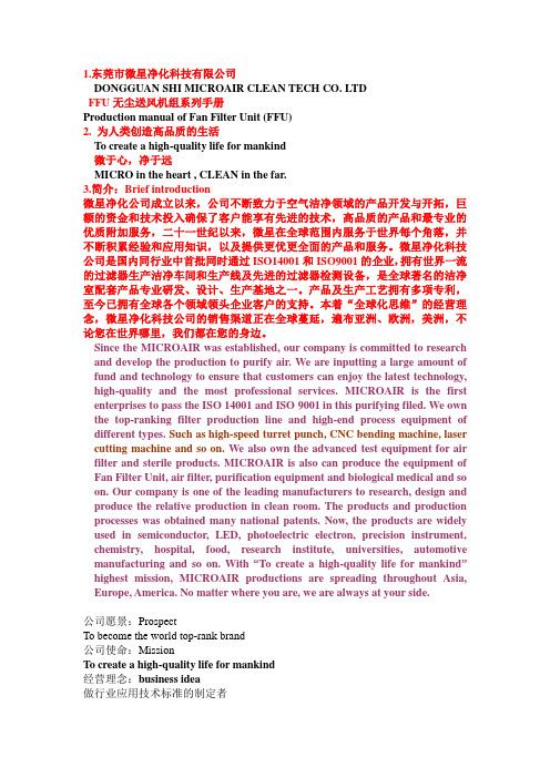
1.东莞市微星净化科技有限公司DONGGUAN SHI MICROAIR CLEAN TECH CO. LTDFFU无尘送风机组系列手册Production manual of Fan Filter Unit (FFU)2. 为人类创造高品质的生活To create a high-quality life for mankind微于心,净于远MICRO in the heart , CLEAN in the far.3.简介:Brief introduction微星净化公司成立以来,公司不断致力于空气洁净领域的产品开发与开拓,巨额的资金和技术投入确保了客户能享有先进的技术,高品质的产品和最专业的优质附加服务,二十一世纪以来,微星在全球范围内服务于世界每个角落,并不断积累经验和应用知识,以及提供更优更全面的产品和服务。
微星净化科技公司是国内同行业中首批同时通过ISO14001和ISO9001的企业,拥有世界一流的过滤器生产洁净车间和生产线及先进的过滤器检测设备,是全球著名的洁净室配套产品专业研发、设计、生产基地之一。
产品及生产工艺拥有多项专利,至今已拥有全球各个领域领头企业客户的支持。
本着“全球化思维”的经营理念,微星净化科技公司的销售渠道正在全球蔓延,遍布亚洲、欧洲,美洲,不论您在世界哪里,我们都在您的身边。
Since the MICROAIR was established, our company is committed to research and develop the production to purify air. We are inputting a large amount of fund and technology to ensure that customers can enjoy the latest technology, high-quality and the most professional services. MICROAIR is the first enterprises to pass the ISO 14001 and ISO 9001 in this purifying filed. We own the top-ranking filter production line and high-end process equipment of different types. Such as high-speed turret punch, CNC bending machine, laser cutting machine and so on. We also own the advanced test equipment for air filter and sterile products. MICROAIR is also can produce the equipment of Fan Filter Unit, air filter, purification equipment and biological medical and so on. Our company is one of the leading manufacturers to research, design and produce the relative production in clean room. The products and production processes was obtained many national patents. Now, the products are widely used in semiconductor, LED, photoelectric electron, precision instrument, chemistry, hospital, food, research institute, universities, automotive manufacturing and so on. With “To create a high-quality life for mankind”highest mission, MICROAIR productions are spreading throughout Asia, Europe, America. No matter where you are, we are always at your side.公司愿景:ProspectTo become the world top-rank brand公司使命:MissionTo create a high-quality life for mankind经营理念:business idea做行业应用技术标准的制定者Be the standard makers of application technology提供优异的空气净化应用技术方案Provide excellent air clean application scheme持续不断的为顾客创造价值Continuate to create value for customers4.生产设备:production equipment5.案例展示:case presentation6.无尘送风机组:Fan Filter Unit (FFU)适用领域:application无尘送风机组系列产品主要用途是净化送入洁净区的空气,以达到洁净环境的要求。
2017附件.

方远强 中国轻工业长沙工程有限公司 张昌民 蒲长均 黄桃仙 龚含军 翁榕安 李晓燕 周艳容 柳霞 时格格 刘创奇 谭家斌 李威 刘钦文 黄锐 刘刚毅 刘刚毅 曾海涛 何清 何清 邹宇 王文宇 张文志 佘盾 彭秋香 张凯 唐歆洁
30 31 32 33 34 35 36 37 38 39 40 41 42 43 44 45 46 47 48 49 50 51 52 53 54 55 56 57 58 59
齐安平 株洲神禹水利水电建筑有限公司 黎瑞虹 湖南雁星建筑工程有限公司 尹彬 徐玄 湖南省第四工程有限公司 中南大学
邓俊群 长沙凯迪机械有限公司 贾谊 建行长沙铁银支行
吴科德 宁乡县交通局 陈伟 韩冰 袁芳 望城县房屋产权管理局 湖南信息科学职业学院 湖南工程职业技术学院
张笑言 湖南大众传媒职业技术学院 应煌 胡馨 中国南方航空湖南分公司 湖南联合教育出版物发行有限公司
姓名
单位
备注 补审 补审 补审 补办证书 补办证书 补办证书 补办证书 补办证书 补办证书 补办证书 补办证书 补办证书 补办证书 补办证书 补办证书 补办证书 补办证书 补办证书 补办证书 补办证书 补办证书 补办证书 补办证书 补办证书 补办证书 补办证书 补办证书 补办证书 补办证书
- 1、下载文档前请自行甄别文档内容的完整性,平台不提供额外的编辑、内容补充、找答案等附加服务。
- 2、"仅部分预览"的文档,不可在线预览部分如存在完整性等问题,可反馈申请退款(可完整预览的文档不适用该条件!)。
- 3、如文档侵犯您的权益,请联系客服反馈,我们会尽快为您处理(人工客服工作时间:9:00-18:30)。
公司简介四川沃特尔水处理设备有限公司位于成都市青羊工业园模具园四区A6栋,是国际领先的水处理系统解决方案提供商,是集水处理产品的开发与设计、设备生产与销售、工程配套与安装、技术咨询与服务为一体的新型环保企业。
公司拥有3000多平方米的标准化厂房,在全国各主要城市建立了完善健全的营销网络和售后服务网络,在企业运营的各个环节严格遵循ISO9001质量管理体系标准,为用户提供一系列的高品质产品和全面及时的零部件供应。
公司下设【总经办】、【综合行政部】、【财务审计部】、【销售部】、【生产部】、【技术研发部】、【质量部】、【售后服务部】八个部门,公司汇集了一大批精英人才,为广大客户及同行提供更加细致、更加专业的全面服务,专门为您提供:(1)实验室专用超纯水机系列:广泛应用于高校、医院、企业、行政检测机构、冶金、有色金属、化工、化妆品、医药卫生、保健品、食品、饮料、啤酒、烟草等各个行业的质检实验室或研发实验室。
(2)工业水处理设备:化工、电子、电镀、制药、食品、饮料、化妆品、医疗卫生、汽车、冶金、电力等行业生产所用的软化水、纯水、超纯水设备。
(3)医院专用纯水设备:医院检验科的全自动生化分析仪、全自动化学发光免疫分析系统配套专用纯水机;医院供应室的全自动清洗消毒机配套专用水处理设备;(4)家用水处理系统:家用纯水机、净水器、软水器;厂矿、学校饮用水系统(直饮水、纯水、净水设备、智能IC卡控制系统);分质供水系统(社区、楼宇、公共场所的自来水深度净化处理设备);商用水处理系统(纯净水、矿泉水、瓶(桶)装水厂的生产设备);以人为本是沃特尔公司永恒的主题,顾客至上是沃特尔公司发展的基石。
全心全意为客户服务,急客户之所急,想客户之所想。
沃特尔公司在提高经营管理和服务水平的同时,不断吸收、培养高素质的服务人才,保证了公司专业化的服务质量。
现今,随着全国市场的全面启动,沃特尔公司将更加规范化、专业化、规模化地为广大客户提供优质、快捷、全方位的服务。
型号:WP-RO-10B WP-RO-20B WP-RO-30B WP-RO-40B适用范围:适用于普通实验、配制常备溶液、基础实验、微生物检验、常规化学分析、进口超纯水机前置配套、盐雾箱配套用水等。
技术参数:1.进水水源:城市自来水,水温1-45℃,水压0.1-0.5Mpa,TDS<300ppm;2.制水量: 10L/H、20L/H、30L/H、40L/H(四种规格可任选一款);3.瞬间取水量:1.5-2L/min;4.出水水质:电导率≤0.2μs/cm@25℃,脱盐率≥99%,水质优于GB/T6682-2008二级水标准;5.电源: 220V/50Hz,功率: 30W-75W,噪音≤40(dB);6.主机尺寸: 长×宽×高(420mm×370mm×470mm),重量: 25kg;功能特点:1.一键式按键操作设计,简单、快捷、方便;2.系统具备缺水停机保护、停电自动复位、满水自动停机、超低压保护、开机自动冲洗等功能;3. LCD背光液晶电导率仪随时在线检测并准确直观地显示出水水质;4.采用可调压RO静音增压泵(提供CE认证),可连续运转10000小时以上;5.采用内置WATER大容量一体式双通道注塑型预处理+纯化柱系统,使用寿命更长;6.配置20L进口真空压力储水桶(通过NSF认证),避免了与空气接触的二次污染。
五、选配:1.原水增压系统(原水水压不足时选配);2.全自动软水器(原水TDS>300ppm时选配);型号:WP-ROL-45 WP-ROL-60 WP-ROL-80 WP-ROL-100适用范围:适用于高校学生实验集中供水、设备冲洗用水、中心化验室用水、配制常备溶液、基础实验、微生物检验、常规化学分析、进口超纯水机前置配套、盐雾箱配套用水等。
技术参数:1.进水水源:城市自来水,水温1-45℃,水压0.1-0.5Mpa,TDS<300ppm;2.制水量: 45L/H、60L/H、80L/H、100L/H(四种规格可任选一款);3.瞬间取水量:2-3L/min;4.出水水质: 电导率≤0.2μs/cm@25℃,脱盐率≥99%,水质优于GB/T6682-2008二级水标准;5.电源: 220V/50Hz,功率: 50W-100W,噪音≤40(dB);6.主机尺寸: 长×宽×高(470mm×390mm×860mm),重量:45kg;功能特点:1.单片机微电脑全自动控制程序设计,触摸按键操作系统;2.系统具备开机自检、缺水停机报警、停电自动复位、满水自动停机、超低压保护、RO膜自动冲洗等功能;3.LCD背光液晶电导率仪随时在线检测并准确直观地显示出水水质;4.采用可调压RO静音增压泵(提供CE认证),可连续运转10000小时以上;5.采用内置WATER大容量一体式双通道注塑型预处理+纯化柱系统,使用寿命更长;6.配置42L进口真空压力储水桶(通过NSF认证),避免了与空气接触的二次污染;7.系统具备操作适时真人语音播报功能,更能体现机器的人性化设计;8.系统配备反渗透压力监测表,可随时通过压力判断反渗透膜的运行压力及污堵程度。
选配:1.原水增压系统(原水水压不足时选配);2.全自动软水器(原水TDS>300ppm时选配);普通型实验室专用超纯水机型号:WP-UP-1810 WP-UP-1820 WP-UP-1830 WP-UP-1840适用范围:适用于标准实验、痕量分析、原子吸收、荧光分析、生化分析、环境分析、血清检查、气相色谱及高效液相等。
技术参数:1.进水水源:城市自来水,水温1-45℃,水压0.1-0.5Mpa,TDS<300ppm;2.制水量: 10L/H、20L/H、30L/H、40L/H(四种规格可任选一款);3.瞬间取水量:1.5-2L/min;4.出水水质: 电阻率18.25MΩ.cm@25℃,水质达到美国CAP、ASTM、NCCLS标准及中国国家电子一级超纯水标准;可溶性硅[以(SiO2)计]:<0.01mg/L;吸光度(254nm,1cm光程):≤0.001;微粒子/颗粒物(大于0.1μm)含量:<1/ml;热源含量:<0.005Eu/ml;微生物/菌落数含量:<1cfu/ml;总有机碳量TOC:≤5ppb;金属阳离子含量(单位PPb):Fe(铁)<0.005 Cu(铜)<0.005 Al(铝)<0.005 Ni(镍)<0.005Zn(锌)<0.02 Cr(铬)<0.005 Na(钠)<0.01 K(钾)<0.02阴离子含量(单位PPb):Cl-(氯)<0.01 NO2-(亚硝酸根)<0.02 NO3-(硝酸根)<0.02 SO42-(硫酸根)<0.015.电源: 220V/50Hz,功率: 30W-75W,噪音≤40(dB);6.主机尺寸: 长×宽×高(420mm×370mm×470mm),重量: 25kg;功能特点:1.一键式按键操作设计,简单、快捷、方便;2.系统具备缺水停机保护、停电自动复位、满水自动停机、超低压保护、开机自动冲洗等功能;3. LCD背光液晶电阻率仪随时在线检测并准确直观地显示出水水质;4.采用可调压RO静音增压泵(提供CE认证),可连续运转10000小时以上;5.采用内置WATER大容量一体式双通道注塑型预处理+纯化柱系统,使用寿命更长;6.配置20L进口真空压力储水桶(通过NSF认证),避免了与空气接触的二次污染。
选配:1.原水增压系统(原水水压不足时选配);2.全自动软水器(原水TDS>300ppm时选配);微量元素型实验室专用超纯水机型号:WP-Z-UP WP-Z-UV适用范围:适用于标准实验、痕量分析、原子吸收、荧光分析、生化分析、环境分析、血清检查、气相色谱及高效液相等。
技术参数:1.进水水源:纯净水、去离子水、蒸馏水等,电导率<10μs/cm@25℃;2.制水量:2L/min;3.出水水质: 电阻率18.25MΩ.cm@25℃,水质达到美国CAP、ASTM、NCCLS标准及中国国家电子一级超纯水标准;可溶性硅[以(SiO2)计]:<0.01mg/L;吸光度(254nm,1cm光程):≤0.001;微粒子/颗粒物(大于0.1μm)含量:<1/ml;热源含量:<0.005Eu/ml;微生物/菌落数含量:<1cfu/ml;总有机碳量TOC:≤5ppb;金属阳离子含量(单位PPb):Fe(铁)<0.005 Cu(铜)<0.005 Al(铝)<0.005 Ni(镍)<0.005Zn(锌)<0.02 Cr(铬)<0.005 Na(钠)<0.01 K(钾)<0.02阴离子含量(单位PPb):Cl-(氯)<0.01 NO2-(亚硝酸根)<0.02 NO3-(硝酸根)<0.02 SO42-(硫酸根)<0.014.电源: 220V/50Hz,功率: 30W-75W,噪音≤40(dB);5.主机尺寸: 长×宽×高(420mm×370mm×470mm),重量: 25kg;功能特点:1.一键式按键操作设计,简单、快捷、方便;2.系统具备缺水停机保护、停电自动复位、取水自动启动、备用自动停机等功能;3. LCD背光液晶电阻率仪随时在线检测并准确直观地显示出水水质;4.采用恒压静音自吸供水泵(提供CE认证),可连续运转10000小时以上;5.采用内置WATER大容量双通道纯化柱系统,使用寿命更长;6.配备40L大容量原水箱,液位控制缺水停机保护;7.配置UV双波长185nm和254nm的紫外消解系统(UV型标配)。
8.配置原装德国进口0.22μm终端囊式热源过滤器(选配)。
标准型实验室专用超纯水机型号:WP-UPT-10 WP-UPT-20 WP-UPT-30 WP-UPT-40适用范围:适用于HPLC、TOC、PCR、AAS、ICP、ICP-MS、气相色谱、氨基酸分析等。
技术参数:1.进水水源:城市自来水,水温1-45℃,水压0.1-0.5Mpa,TDS<300ppm;2.制水量: 10L/H、20L/H、30L/H、40L/H(四种规格可任选一款);3.瞬间取水量:1.5-2L/min;4. 出水水质:(1)RO水电导率:1-10μs/cm@25℃,脱盐率≥99%,水质达到GB/T6682-2008三级水标准;(2)UP超纯水电阻率:18.25MΩ.cm@25℃,水质达到美国CAP、ASTM、NCCLS标准及中国国家电子一级超纯水标准;可溶性硅[以(SiO2)计]:<0.01mg/L;吸光度(254nm,1cm光程):≤0.001;微粒子/颗粒物(大于0.1μm)含量:<1/ml;热源含量:<0.005Eu/ml;微生物/菌落数含量:<1cfu/ml;总有机碳量TOC:≤5ppb;金属阳离子含量(单位PPb):Fe(铁)<0.005 Cu(铜)<0.005 Al(铝)<0.005 Ni(镍)<0.005Zn(锌)<0.02 Cr(铬)<0.005 Na(钠)<0.01 K(钾)<0.02阴离子含量(单位PPb):Cl-(氯)<0.01 NO2-(亚硝酸根)<0.02 NO3-(硝酸根)<0.02 SO42-(硫酸根)<0.015.电源: 220V/50Hz,功率: 30W-75W,噪音≤40(dB);6.主机尺寸: 长×宽×高(460mm×380mm×510mm);重量: 30kg;功能特点:1.微电脑全自动控制设计,LCD大屏幕中文彩色液晶屏显示,设备运行状态一目了然,人机对话功能完备;2.系统具备两个取水口,一机两用,可同时产出RO纯水和UP超纯水;3.系统具备开机自检、自动循环冲洗排放、缺水报警、停电自动复位、满水自动停机、超低压保护等功能;4.系统具备UP超纯水超标排放设定功能、耗材失效语音报警及更换提示功能;5.系统具备UP超纯水电阻率、总有机碳量(TOC)在线检测显示功能;6.配置20L进口真空压力储水桶(通过NSF认证),避免了与空气接触的二次污染;7.采用内置WATER大容量一体式双通道注塑型预处理+纯化柱系统,使用寿命更长;8.系统具备0-9999ml定时定量取水功能;9.系统具备操作适时真人语音播报功能,更能体现机器的人性化设计;10.系统具备历史数据储存查询功能,能有效准确地记录并查询历次取水时间(年/月/日/时/分)、取水量(ml) 及取水水质(纯水电导率及超纯水电阻率)等历史数据;11.系统具备定时开/关机功能,用户可任意设定开机或关机时间,同时具有当前日期显示与时钟显示及设定功能;12.系统具备二级PIN密码保护,可设置开机密码及用户操作密码,设备管理权和使用权分开,防止无关人员操作。