1-DM_12_CH01_intro
LTE_3GPP_36.213-860(中文版)
3GPP
Release 8
3
3GPP TS 36.213 V8.6.0 (2009-03)
Contents
Foreword ...................................................................................................................................................... 5 1 2 3
Internet
Copyright Notification No part may be reproduced except as authorized by written permission. The copyright and the foregoing restriction extend to reproduction in all media.
© 2009, 3GPP Organizational Partners (ARIB, ATIS, CCSA, ETSI, TTA, TTC). All rights reserved. UMTS™ is a Trade Mark of ETSI registered for the benefit of its members 3GPP™ is a Trade Mark of ETSI registered for the benefit of its Members and of the 3GPP Organizational Partners LTE™ is a Trade Mark of ETSI currently being registered for the benefit of i ts Members and of the 3GPP Organizational Partners GSM® and the GSM logo are registered and owned by the GSM Association
Converge SR 1212A数字矩阵混音器与四通道电源放大器数据资料说明书
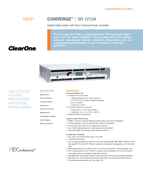
Converge TM|SR 1212ADigital Matrix Mixer with Four Channel Power AmplifierConverge Pro DATA SHeeT <THE ULTIMATE IN AUDIO PROCESSING AND DIGITAL MATRIX MIXING APPLICATIonSBoardroomsTraining CentersMunicipal RoomsCourtroomsHouses of WorshipTelemedicinePresentation SystemsZoned PagingMasking SystemsADvAnTAgeSAdvanced Feature SetManagement Improvements+Integrated Ethernet and USB connections>SNMP and HTML remote management agents>Event scheduler>Diagnostic console>Simplified Configuration Software+Drag & drop A/V and channel objects>Selectable views -- unit, matrix, channel>Expanded serial command set+Superior Audio PerformanceDARE™ (Dynamic Automatic Resonance Elimination) for control of feedback+Unique automatic mixing process delivers optimum intelligibility+20 Hz-22 kHz bandwidth for full-range audio response+ALC & AGC keep participants’ audio balanced and consistent+Advanced Digital Processing on each amplifier channel+Configuration FlexibilityFour built-in 35 Watt amplifiers, 8Ω or 70V/100V+Up to 96 microphones+Link multiple Converge/Converge Pro units (Converge Pro 880, 880T, 880TA, 840T, 8i, TH20,+Converge SR 1212 and SR 1212A) for extensive microphone coverage and up to 16 phonelinesEnhanced expansion bus, featuring 18 mix-minus audio buses for routing between units+Ten mic gating groups (four internal & six global) allow separation of mics into individual+mixer gating groups for greater configuration flexibility32 presets can be executed on-the-fly without disturbing other ongoing preset operations+255 Macros for customized audio control/configuration with single command execution+No space required between rack mounted units+NEw!Audio PerformanceConditions: Unless otherwise specified,all measurements are performedfrom 20 Hz to 22 kHz Bw limit (no weighting)Frequency Response: 20 Hz to 22 kHz+/- 1 dBNoise (EIN): -126 dBu, 20 kHz Bw,max gainRs= 150ΩTHD+ Noise: <0.02%Dynamic Range: >105 dB (non A weighted)Crosstalk: <-91 dB re 20 dBu full band. Mic/Line Inputs 1-8Push-on mini-terminal block, balanced, bridgingImpedance: > 5 KΩNominal Level: adjustable -56 dBu to 0 dBu (7dB step coarse gain adjustment) Maximum Level: -65 to +20 dBu Phantom Power: 24V, selectableLine Inputs 9-12Push-on mini-terminal block, balanced, bridgingImpedance: > 5 KΩNominal Level: 0 dBuMaximum Level: 20 dBuoutput 1-8Push-on mini-terminal block, balanced, bridgingImpedance: < 50ΩNominal Level: 0 dBuMaximum Level: 20 dBuAuto Mixer ParametersNumber of Open Microphones (NOM)PA Adaptive ModeFirst Mic Priority ModeMaximum # of MicsAmbient LevelGate Threshold AdjustOff Attenuation AdjustHold TimeDecay RateChairman Override96 T otal Microphones per site6- Global Gating Groups4- Internal Gating Groups Matrix Mixing Parameters8- Microphone Analog Inputs4- Analog Line Inputs8- Analog Line Outputs4- Power Amplifier Outputs18- Expansion Bus in/out8- Assignable Processing Blocks in/outAssignable Processing BlocksFiltersAll PassLow PassHigh PassLow shelvingHigh shelvingPEQNotchCrossoversCD HornCompressorDelay: adjustable up to 250 msPower Amplifier output ProcessingFeedBack Elimination w/ring cancellation10-band EQ filter4-node filter bank for CrossoverDelay BlockCompressor/LimiterNoise Gate for Hiss ControlSound Masking Generator per channelAdaptive Volume ControlMulti Channel ControlMicrophone Processing4-node filter bankAGC/ALCPower AmplifiersChannels: 4Amplifier Output: 4x35 Watts into 8ΩImpedance: Selectable 8Ω, 70V, 100VTHD + Noise: <0.2% (1/3 Power)Crosstalk: <-68 dBexpansion BusConnection: CAT 5, RJ45Mix Minus Structure18 Audio Buses6 Gating Buses8 Reference Busesnetwork10/100 Auto Switching (PC andNetwork Port)HTTP ServerT elnet ClientSNMP AgentSMTP ClientDNSDHCPrS-232DB-99.6k – 115k baud8/1/0Hardware Flow ControlUSBVersion 2.0 compatibleT ype: B-connectorgPIoDB 25 female (A/B)Inputs: Active LowOutputs: Open Collector, 40Vdc, 40 mAPower100-240VAC; 50/60 Hz,300 watts (maximum)Idle: 139 BTU/hrFull Load: 779 BTU/hrEfficiency: >80%Humidity15 to 80%MechanicalDimensions: 2RU3.5” H x 17.25” w x 15.92” Dweight: < 30 lbs.environmentalOperating temperature:32-122 degrees FComplianceFCCIndustry CanadaCERoHSClass 2 wiring RequiredPart number910-151-901 Converge SR 1212ACONVERGE PRO SR 1212A DATA SHeeT <> Converge Pro Sr 1212A BACK PAneL > SPeCIFICATIonS> CLeArone LoCATIonSHeadquarters:Salt Lake City, UT USA 5225 wiley Post way Suite 500Salt Lake City, UT 84116 Tel: 801-975-7200T oll Free: 800-945-7730 Fax: 801-977-0087******************Latin AmericaTel: 801-974-3621*******************EMEATel: 44 (0) 1189 036 053*******************APACTel: 801-303-3388*******************Other product names may be registered trademarks of their respective owners who do not necessarily endorse ClearOne or ClearOne’s products. All rights reserved. Information in this document subject to change without notice.© ClearOne. 802-151-901-DS Revision 1.9。
NuMicro N9H30系列开发板用户手册说明书
NuMicro®FamilyArm® ARM926EJ-S BasedNuMaker-HMI-N9H30User ManualEvaluation Board for NuMicro® N9H30 SeriesNUMAKER-HMI-N9H30 USER MANUALThe information described in this document is the exclusive intellectual property ofNuvoton Technology Corporation and shall not be reproduced without permission from Nuvoton.Nuvoton is providing this document only for reference purposes of NuMicro microcontroller andmicroprocessor based system design. Nuvoton assumes no responsibility for errors or omissions.All data and specifications are subject to change without notice.For additional information or questions, please contact: Nuvoton Technology Corporation.Table of Contents1OVERVIEW (5)1.1Features (7)1.1.1NuMaker-N9H30 Main Board Features (7)1.1.2NuDesign-TFT-LCD7 Extension Board Features (7)1.2Supporting Resources (8)2NUMAKER-HMI-N9H30 HARDWARE CONFIGURATION (9)2.1NuMaker-N9H30 Board - Front View (9)2.2NuMaker-N9H30 Board - Rear View (14)2.3NuDesign-TFT-LCD7 - Front View (20)2.4NuDesign-TFT-LCD7 - Rear View (21)2.5NuMaker-N9H30 and NuDesign-TFT-LCD7 PCB Placement (22)3NUMAKER-N9H30 AND NUDESIGN-TFT-LCD7 SCHEMATICS (24)3.1NuMaker-N9H30 - GPIO List Circuit (24)3.2NuMaker-N9H30 - System Block Circuit (25)3.3NuMaker-N9H30 - Power Circuit (26)3.4NuMaker-N9H30 - N9H30F61IEC Circuit (27)3.5NuMaker-N9H30 - Setting, ICE, RS-232_0, Key Circuit (28)NUMAKER-HMI-N9H30 USER MANUAL3.6NuMaker-N9H30 - Memory Circuit (29)3.7NuMaker-N9H30 - I2S, I2C_0, RS-485_6 Circuit (30)3.8NuMaker-N9H30 - RS-232_2 Circuit (31)3.9NuMaker-N9H30 - LCD Circuit (32)3.10NuMaker-N9H30 - CMOS Sensor, I2C_1, CAN_0 Circuit (33)3.11NuMaker-N9H30 - RMII_0_PF Circuit (34)3.12NuMaker-N9H30 - RMII_1_PE Circuit (35)3.13NuMaker-N9H30 - USB Circuit (36)3.14NuDesign-TFT-LCD7 - TFT-LCD7 Circuit (37)4REVISION HISTORY (38)List of FiguresFigure 1-1 Front View of NuMaker-HMI-N9H30 Evaluation Board (5)Figure 1-2 Rear View of NuMaker-HMI-N9H30 Evaluation Board (6)Figure 2-1 Front View of NuMaker-N9H30 Board (9)Figure 2-2 Rear View of NuMaker-N9H30 Board (14)Figure 2-3 Front View of NuDesign-TFT-LCD7 Board (20)Figure 2-4 Rear View of NuDesign-TFT-LCD7 Board (21)Figure 2-5 Front View of NuMaker-N9H30 PCB Placement (22)Figure 2-6 Rear View of NuMaker-N9H30 PCB Placement (22)Figure 2-7 Front View of NuDesign-TFT-LCD7 PCB Placement (23)Figure 2-8 Rear View of NuDesign-TFT-LCD7 PCB Placement (23)Figure 3-1 GPIO List Circuit (24)Figure 3-2 System Block Circuit (25)Figure 3-3 Power Circuit (26)Figure 3-4 N9H30F61IEC Circuit (27)Figure 3-5 Setting, ICE, RS-232_0, Key Circuit (28)Figure 3-6 Memory Circuit (29)Figure 3-7 I2S, I2C_0, RS-486_6 Circuit (30)Figure 3-8 RS-232_2 Circuit (31)Figure 3-9 LCD Circuit (32)NUMAKER-HMI-N9H30 USER MANUAL Figure 3-10 CMOS Sensor, I2C_1, CAN_0 Circuit (33)Figure 3-11 RMII_0_PF Circuit (34)Figure 3-12 RMII_1_PE Circuit (35)Figure 3-13 USB Circuit (36)Figure 3-14 TFT-LCD7 Circuit (37)List of TablesTable 2-1 LCD Panel Combination Connector (CON8) Pin Function (11)Table 2-2 Three Sets of Indication LED Functions (12)Table 2-3 Six Sets of User SW, Key Matrix Functions (12)Table 2-4 CMOS Sensor Connector (CON10) Function (13)Table 2-5 JTAG ICE Interface (J2) Function (14)Table 2-6 Expand Port (CON7) Function (16)Table 2-7 UART0 (J3) Function (16)Table 2-8 UART2 (J6) Function (16)Table 2-9 RS-485_6 (SW6~8) Function (17)Table 2-10 Power on Setting (SW4) Function (17)Table 2-11 Power on Setting (S2) Function (17)Table 2-12 Power on Setting (S3) Function (17)Table 2-13 Power on Setting (S4) Function (17)Table 2-14 Power on Setting (S5) Function (17)Table 2-15 Power on Setting (S7/S6) Function (18)Table 2-16 Power on Setting (S9/S8) Function (18)Table 2-17 CMOS Sensor Connector (CON9) Function (19)Table 2-18 CAN_0 (SW9~10) Function (19)NUMAKER-HMI-N9H30 USER MANUAL1 OVERVIEWThe NuMaker-HMI-N9H30 is an evaluation board for GUI application development. The NuMaker-HMI-N9H30 consists of two parts: a NuMaker-N9H30 main board and a NuDesign-TFT-LCD7 extensionboard. The NuMaker-HMI-N9H30 is designed for project evaluation, prototype development andvalidation with HMI (Human Machine Interface) function.The NuMaker-HMI-N9H30 integrates touchscreen display, voice input/output, rich serial port serviceand I/O interface, providing multiple external storage methods.The NuDesign-TFT-LCD7 can be plugged into the main board via the DIN_32x2 extension connector.The NuDesign-TFT-LCD7 includes one 7” LCD which the resolution is 800x480 with RGB-24bits andembedded the 4-wires resistive type touch panel.Figure 1-1 Front View of NuMaker-HMI-N9H30 Evaluation BoardNUMAKER-HMI-N9H30 USER MANUAL Figure 1-2 Rear View of NuMaker-HMI-N9H30 Evaluation Board1.1 Features1.1.1 NuMaker-N9H30 Main Board Features●N9H30F61IEC chip: LQFP216 pin MCP package with DDR (64 MB)●SPI Flash using W25Q256JVEQ (32 MB) booting with quad mode or storage memory●NAND Flash using W29N01HVSINA (128 MB) booting or storage memory●One Micro-SD/TF card slot served either as a SD memory card for data storage or SDIO(Wi-Fi) device●Two sets of COM ports:–One DB9 RS-232 port with UART_0 used 75C3232E transceiver chip can be servedfor function debug and system development.–One DB9 RS-232 port with UART_2 used 75C3232E transceiver chip for userapplication●22 GPIO expansion ports, including seven sets of UART functions●JTAG interface provided for software development●Microphone input and Earphone/Speaker output with 24-bit stereo audio codec(NAU88C22) for I2S interfaces●Six sets of user-configurable push button keys●Three sets of LEDs for status indication●Provides SN65HVD230 transceiver chip for CAN bus communication●Provides MAX3485 transceiver chip for RS-485 device connection●One buzzer device for program applicationNUMAKER-HMI-N9H30 USER MANUAL●Two sets of RJ45 ports with Ethernet 10/100 Mbps MAC used IP101GR PHY chip●USB_0 that can be used as Device/HOST and USB_1 that can be used as HOSTsupports pen drives, keyboards, mouse and printers●Provides over-voltage and over current protection used APL3211A chip●Retain RTC battery socket for CR2032 type and ADC0 detect battery voltage●System power could be supplied by DC-5V adaptor or USB VBUS1.1.2 NuDesign-TFT-LCD7 Extension Board Features●7” resolution 800x480 4-wire resistive touch panel for 24-bits RGB888 interface●DIN_32x2 extension connector1.2 Supporting ResourcesFor sample codes and introduction about NuMaker-N9H30, please refer to N9H30 BSP:https:///products/gui-solution/gui-platform/numaker-hmi-n9h30/?group=Software&tab=2Visit NuForum for further discussion about the NuMaker-HMI-N9H30:/viewforum.php?f=31 NUMAKER-HMI-N9H30 USER MANUALNUMAKER-HMI-N9H30 USER MANUAL2 NUMAKER-HMI-N9H30 HARDWARE CONFIGURATION2.1 NuMaker-N9H30 Board - Front View Combination Connector (CON8)6 set User SWs (K1~6)3set Indication LEDs (LED1~3)Power Supply Switch (SW_POWER1)Audio Codec(U10)Microphone(M1)NAND Flash(U9)RS-232 Transceiver(U6, U12)RS-485 Transceiver(U11)CAN Transceiver (U13)Figure 2-1 Front View of NuMaker-N9H30 BoardFigure 2-1 shows the main components and connectors from the front side of NuMaker-N9H30 board. The following lists components and connectors from the front view:NuMaker-N9H30 board and NuDesign-TFT-LCD7 board combination connector (CON8). This panel connector supports 4-/5-wire resistive touch or capacitance touch panel for 24-bits RGB888 interface.Connector GPIO pin of N9H30 FunctionCON8.1 - Power 3.3VCON8.2 - Power 3.3VCON8.3 GPD7 LCD_CSCON8.4 GPH3 LCD_BLENCON8.5 GPG9 LCD_DENCON8.7 GPG7 LCD_HSYNCCON8.8 GPG6 LCD_CLKCON8.9 GPD15 LCD_D23(R7)CON8.10 GPD14 LCD_D22(R6)CON8.11 GPD13 LCD_D21(R5)CON8.12 GPD12 LCD_D20(R4)CON8.13 GPD11 LCD_D19(R3)CON8.14 GPD10 LCD_D18(R2)CON8.15 GPD9 LCD_D17(R1)CON8.16 GPD8 LCD_D16(R0)CON8.17 GPA15 LCD_D15(G7)CON8.18 GPA14 LCD_D14(G6)CON8.19 GPA13 LCD_D13(G5)CON8.20 GPA12 LCD_D12(G4)CON8.21 GPA11 LCD_D11(G3)CON8.22 GPA10 LCD_D10(G2)CON8.23 GPA9 LCD_D9(G1) NUMAKER-HMI-N9H30 USER MANUALCON8.24 GPA8 LCD_D8(G0)CON8.25 GPA7 LCD_D7(B7)CON8.26 GPA6 LCD_D6(B6)CON8.27 GPA5 LCD_D5(B5)CON8.28 GPA4 LCD_D4(B4)CON8.29 GPA3 LCD_D3(B3)CON8.30 GPA2 LCD_D2(B2)CON8.31 GPA1 LCD_D1(B1)CON8.32 GPA0 LCD_D0(B0)CON8.33 - -CON8.34 - -CON8.35 - -CON8.36 - -CON8.37 GPB2 LCD_PWMCON8.39 - VSSCON8.40 - VSSCON8.41 ADC7 XPCON8.42 ADC3 VsenCON8.43 ADC6 XMCON8.44 ADC4 YMCON8.45 - -CON8.46 ADC5 YPCON8.47 - VSSCON8.48 - VSSCON8.49 GPG0 I2C0_CCON8.50 GPG1 I2C0_DCON8.51 GPG5 TOUCH_INTCON8.52 - -CON8.53 - -CON8.54 - -CON8.55 - -NUMAKER-HMI-N9H30 USER MANUAL CON8.56 - -CON8.57 - -CON8.58 - -CON8.59 - VSSCON8.60 - VSSCON8.61 - -CON8.62 - -CON8.63 - Power 5VCON8.64 - Power 5VTable 2-1 LCD Panel Combination Connector (CON8) Pin Function●Power supply switch (SW_POWER1): System will be powered on if the SW_POWER1button is pressed●Three sets of indication LEDs:LED Color DescriptionsLED1 Red The system power will beterminated and LED1 lightingwhen the input voltage exceeds5.7V or the current exceeds 2A.LED2 Green Power normal state.LED3 Green Controlled by GPH2 pin Table 2-2 Three Sets of Indication LED Functions●Six sets of user SW, Key Matrix for user definitionKey GPIO pin of N9H30 FunctionK1 GPF10 Row0 GPB4 Col0K2 GPF10 Row0 GPB5 Col1K3 GPE15 Row1 GPB4 Col0K4 GPE15 Row1 GPB5 Col1K5 GPE14 Row2 GPB4 Col0K6GPE14 Row2GPB5 Col1 Table 2-3 Six Sets of User SW, Key Matrix Functions●NAND Flash (128 MB) with Winbond W29N01HVS1NA (U9)●Microphone (M1): Through Nuvoton NAU88C22 chip sound input●Audio CODEC chip (U10): Nuvoton NAU88C22 chip connected to N9H30 using I2Sinterface–SW6/SW7/SW8: 1-2 short for RS-485_6 function and connected to 2P terminal (CON5and J5)–SW6/SW7/SW8: 2-3 short for I2S function and connected to NAU88C22 (U10).●CMOS Sensor connector (CON10, SW9~10)–SW9~10: 1-2 short for CAN_0 function and connected to 2P terminal (CON11)–SW9~10: 2-3 short for CMOS sensor function and connected to CMOS sensorconnector (CON10)Connector GPIO pin of N9H30 FunctionCON10.1 - VSSCON10.2 - VSSNUMAKER-HMI-N9H30 USER MANUALCON10.3 - Power 3.3VCON10.4 - Power 3.3VCON10.5 - -CON10.6 - -CON10.7 GPI4 S_PCLKCON10.8 GPI3 S_CLKCON10.9 GPI8 S_D0CON10.10 GPI9 S_D1CON10.11 GPI10 S_D2CON10.12 GPI11 S_D3CON10.13 GPI12 S_D4CON10.14 GPI13 S_D5CON10.15 GPI14 S_D6CON10.16 GPI15 S_D7CON10.17 GPI6 S_VSYNCCON10.18 GPI5 S_HSYNCCON10.19 GPI0 S_PWDNNUMAKER-HMI-N9H30 USER MANUAL CON10.20 GPI7 S_nRSTCON10.21 GPG2 I2C1_CCON10.22 GPG3 I2C1_DCON10.23 - VSSCON10.24 - VSSTable 2-4 CMOS Sensor Connector (CON10) FunctionNUMAKER-HMI-N9H30 USER MANUAL2.2NuMaker-N9H30 Board - Rear View5V In (CON1)RS-232 DB9 (CON2,CON6)Expand Port (CON7)Speaker Output (J4)Earphone Output (CON4)Buzzer (BZ1)System ResetSW (SW5)SPI Flash (U7,U8)JTAG ICE (J2)Power ProtectionIC (U1)N9H30F61IEC (U5)Micro SD Slot (CON3)RJ45 (CON12, CON13)USB1 HOST (CON15)USB0 Device/Host (CON14)CAN_0 Terminal (CON11)CMOS Sensor Connector (CON9)Power On Setting(SW4, S2~S9)RS-485_6 Terminal (CON5)RTC Battery(BT1)RMII PHY (U14,U16)Figure 2-2 Rear View of NuMaker-N9H30 BoardFigure 2-2 shows the main components and connectors from the rear side of NuMaker-N9H30 board. The following lists components and connectors from the rear view:● +5V In (CON1): Power adaptor 5V input ●JTAG ICE interface (J2) ConnectorGPIO pin of N9H30Function J2.1 - Power 3.3V J2.2 GPJ4 nTRST J2.3 GPJ2 TDI J2.4 GPJ1 TMS J2.5 GPJ0 TCK J2.6 - VSS J2.7 GPJ3 TD0 J2.8-RESETTable 2-5 JTAG ICE Interface (J2) Function●SPI Flash (32 MB) with Winbond W25Q256JVEQ (U7); only one (U7 or U8) SPI Flashcan be used●System Reset (SW5): System will be reset if the SW5 button is pressed●Buzzer (BZ1): Control by GPB3 pin of N9H30●Speaker output (J4): Through the NAU88C22 chip sound output●Earphone output (CON4): Through the NAU88C22 chip sound output●Expand port for user use (CON7):Connector GPIO pin of N9H30 FunctionCON7.1 - Power 3.3VCON7.2 - Power 3.3VCON7.3 GPE12 UART3_TXDCON7.4 GPH4 UART1_TXDCON7.5 GPE13 UART3_RXDCON7.6 GPH5 UART1_RXDCON7.7 GPB0 UART5_TXDCON7.8 GPH6 UART1_RTSCON7.9 GPB1 UART5_RXDCON7.10 GPH7 UART1_CTSCON7.11 GPI1 UART7_TXDNUMAKER-HMI-N9H30 USER MANUAL CON7.12 GPH8 UART4_TXDCON7.13 GPI2 UART7_RXDCON7.14 GPH9 UART4_RXDCON7.15 - -CON7.16 GPH10 UART4_RTSCON7.17 - -CON7.18 GPH11 UART4_CTSCON7.19 - VSSCON7.20 - VSSCON7.21 GPB12 UART10_TXDCON7.22 GPH12 UART8_TXDCON7.23 GPB13 UART10_RXDCON7.24 GPH13 UART8_RXDCON7.25 GPB14 UART10_RTSCON7.26 GPH14 UART8_RTSCON7.27 GPB15 UART10_CTSCON7.28 GPH15 UART8_CTSCON7.29 - Power 5VCON7.30 - Power 5VTable 2-6 Expand Port (CON7) Function●UART0 selection (CON2, J3):–RS-232_0 function and connected to DB9 female (CON2) for debug message output.–GPE0/GPE1 connected to 2P terminal (J3).Connector GPIO pin of N9H30 Function J3.1 GPE1 UART0_RXDJ3.2 GPE0 UART0_TXDTable 2-7 UART0 (J3) Function●UART2 selection (CON6, J6):–RS-232_2 function and connected to DB9 female (CON6) for debug message output –GPF11~14 connected to 4P terminal (J6)Connector GPIO pin of N9H30 Function J6.1 GPF11 UART2_TXDJ6.2 GPF12 UART2_RXDJ6.3 GPF13 UART2_RTSJ6.4 GPF14 UART2_CTSTable 2-8 UART2 (J6) Function●RS-485_6 selection (CON5, J5, SW6~8):–SW6~8: 1-2 short for RS-485_6 function and connected to 2P terminal (CON5 and J5) –SW6~8: 2-3 short for I2S function and connected to NAU88C22 (U10)Connector GPIO pin of N9H30 FunctionSW6:1-2 shortGPG11 RS-485_6_DISW6:2-3 short I2S_DOSW7:1-2 shortGPG12 RS-485_6_ROSW7:2-3 short I2S_DISW8:1-2 shortGPG13 RS-485_6_ENBSW8:2-3 short I2S_BCLKNUMAKER-HMI-N9H30 USER MANUALTable 2-9 RS-485_6 (SW6~8) FunctionPower on setting (SW4, S2~9).SW State FunctionSW4.2/SW4.1 ON/ON Boot from USB SW4.2/SW4.1 ON/OFF Boot from eMMC SW4.2/SW4.1 OFF/ON Boot from NAND Flash SW4.2/SW4.1 OFF/OFF Boot from SPI Flash Table 2-10 Power on Setting (SW4) FunctionSW State FunctionS2 Short System clock from 12MHzcrystalS2 Open System clock from UPLL output Table 2-11 Power on Setting (S2) FunctionSW State FunctionS3 Short Watchdog Timer OFFS3 Open Watchdog Timer ON Table 2-12 Power on Setting (S3) FunctionSW State FunctionS4 Short GPJ[4:0] used as GPIO pinS4Open GPJ[4:0] used as JTAG ICEinterfaceTable 2-13 Power on Setting (S4) FunctionSW State FunctionS5 Short UART0 debug message ONS5 Open UART0 debug message OFFTable 2-14 Power on Setting (S5) FunctionSW State FunctionS7/S6 Short/Short NAND Flash page size 2KBS7/S6 Short/Open NAND Flash page size 4KBS7/S6 Open/Short NAND Flash page size 8KBNUMAKER-HMI-N9H30 USER MANUALS7/S6 Open/Open IgnoreTable 2-15 Power on Setting (S7/S6) FunctionSW State FunctionS9/S8 Short/Short NAND Flash ECC type BCH T12S9/S8 Short/Open NAND Flash ECC type BCH T15S9/S8 Open/Short NAND Flash ECC type BCH T24S9/S8 Open/Open IgnoreTable 2-16 Power on Setting (S9/S8) FunctionCMOS Sensor connector (CON9, SW9~10)–SW9~10: 1-2 short for CAN_0 function and connected to 2P terminal (CON11).–SW9~10: 2-3 short for CMOS sensor function and connected to CMOS sensorconnector (CON9).Connector GPIO pin of N9H30 FunctionCON9.1 - VSSCON9.2 - VSSCON9.3 - Power 3.3VCON9.4 - Power 3.3V NUMAKER-HMI-N9H30 USER MANUALCON9.5 - -CON9.6 - -CON9.7 GPI4 S_PCLKCON9.8 GPI3 S_CLKCON9.9 GPI8 S_D0CON9.10 GPI9 S_D1CON9.11 GPI10 S_D2CON9.12 GPI11 S_D3CON9.13 GPI12 S_D4CON9.14 GPI13 S_D5CON9.15 GPI14 S_D6CON9.16 GPI15 S_D7CON9.17 GPI6 S_VSYNCCON9.18 GPI5 S_HSYNCCON9.19 GPI0 S_PWDNCON9.20 GPI7 S_nRSTCON9.21 GPG2 I2C1_CCON9.22 GPG3 I2C1_DCON9.23 - VSSCON9.24 - VSSTable 2-17 CMOS Sensor Connector (CON9) Function●CAN_0 Selection (CON11, SW9~10):–SW9~10: 1-2 short for CAN_0 function and connected to 2P terminal (CON11) –SW9~10: 2-3 short for CMOS sensor function and connected to CMOS sensor connector (CON9, CON10)SW GPIO pin of N9H30 FunctionSW9:1-2 shortGPI3 CAN_0_RXDSW9:2-3 short S_CLKSW10:1-2 shortGPI4 CAN_0_TXDSW10:2-3 short S_PCLKTable 2-18 CAN_0 (SW9~10) Function●USB0 Device/HOST Micro-AB connector (CON14), where CON14 pin4 ID=1 is Device,ID=0 is HOST●USB1 for USB HOST with Type-A connector (CON15)●RJ45_0 connector with LED indicator (CON12), RMII PHY with IP101GR (U14)●RJ45_1 connector with LED indicator (CON13), RMII PHY with IP101GR (U16)●Micro-SD/TF card slot (CON3)●SOC CPU: Nuvoton N9H30F61IEC (U5)●Battery power for RTC 3.3V powered (BT1, J1), can detect voltage by ADC0●RTC power has 3 sources:–Share with 3.3V I/O power–Battery socket for CR2032 (BT1)–External connector (J1)●Board version 2.1NUMAKER-HMI-N9H30 USER MANUAL2.3 NuDesign-TFT-LCD7 -Front ViewFigure 2-3 Front View of NuDesign-TFT-LCD7 BoardFigure 2-3 shows the main components and connectors from the Front side of NuDesign-TFT-LCD7board.7” resolution 800x480 4-W resistive touch panel for 24-bits RGB888 interface2.4 NuDesign-TFT-LCD7 -Rear ViewFigure 2-4 Rear View of NuDesign-TFT-LCD7 BoardFigure 2-4 shows the main components and connectors from the rear side of NuDesign-TFT-LCD7board.NuMaker-N9H30 and NuDesign-TFT-LCD7 combination connector (CON1).NUMAKER-HMI-N9H30 USER MANUAL 2.5 NuMaker-N9H30 and NuDesign-TFT-LCD7 PCB PlacementFigure 2-5 Front View of NuMaker-N9H30 PCB PlacementFigure 2-6 Rear View of NuMaker-N9H30 PCB PlacementNUMAKER-HMI-N9H30 USER MANUALFigure 2-7 Front View of NuDesign-TFT-LCD7 PCB PlacementFigure 2-8 Rear View of NuDesign-TFT-LCD7 PCB Placement3 NUMAKER-N9H30 AND NUDESIGN-TFT-LCD7 SCHEMATICS3.1 NuMaker-N9H30 - GPIO List CircuitFigure 3-1 shows the N9H30F61IEC GPIO list circuit.Figure 3-1 GPIO List Circuit NUMAKER-HMI-N9H30 USER MANUAL3.2 NuMaker-N9H30 - System Block CircuitFigure 3-2 shows the System Block Circuit.NUMAKER-HMI-N9H30 USER MANUALFigure 3-2 System Block Circuit3.3 NuMaker-N9H30 - Power CircuitFigure 3-3 shows the Power Circuit.NUMAKER-HMI-N9H30 USER MANUALFigure 3-3 Power Circuit3.4 NuMaker-N9H30 - N9H30F61IEC CircuitFigure 3-4 shows the N9H30F61IEC Circuit.Figure 3-4 N9H30F61IEC CircuitNUMAKER-HMI-N9H30 USER MANUAL3.5 NuMaker-N9H30 - Setting, ICE, RS-232_0, Key CircuitFigure 3-5 shows the Setting, ICE, RS-232_0, Key Circuit.NUMAKER-HMI-N9H30 USER MANUALFigure 3-5 Setting, ICE, RS-232_0, Key Circuit3.6 NuMaker-N9H30 - Memory CircuitFigure 3-6 shows the Memory Circuit.NUMAKER-HMI-N9H30 USER MANUALFigure 3-6 Memory Circuit3.7 NuMaker-N9H30 - I2S, I2C_0, RS-485_6 CircuitFigure 3-7 shows the I2S, I2C_0, RS-486_6 Circuit.NUMAKER-HMI-N9H30 USER MANUALFigure 3-7 I2S, I2C_0, RS-486_6 Circuit3.8 NuMaker-N9H30 - RS-232_2 CircuitFigure 3-8 shows the RS-232_2 Circuit.NUMAKER-HMI-N9H30 USER MANUALFigure 3-8 RS-232_2 Circuit3.9 NuMaker-N9H30 - LCD CircuitFigure 3-9 shows the LCD Circuit.NUMAKER-HMI-N9H30 USER MANUALFigure 3-9 LCD Circuit3.10 NuMaker-N9H30 - CMOS Sensor, I2C_1, CAN_0 CircuitFigure 3-10 shows the CMOS Sensor,I2C_1, CAN_0 Circuit.NUMAKER-HMI-N9H30 USER MANUALFigure 3-10 CMOS Sensor, I2C_1, CAN_0 Circuit3.11 NuMaker-N9H30 - RMII_0_PF CircuitFigure 3-11 shows the RMII_0_RF Circuit.NUMAKER-HMI-N9H30 USER MANUALFigure 3-11 RMII_0_PF Circuit3.12 NuMaker-N9H30 - RMII_1_PE CircuitFigure 3-12 shows the RMII_1_PE Circuit.NUMAKER-HMI-N9H30 USER MANUALFigure 3-12 RMII_1_PE Circuit3.13 NuMaker-N9H30 - USB CircuitFigure 3-13 shows the USB Circuit.NUMAKER-HMI-N9H30 USER MANUALFigure 3-13 USB Circuit3.14 NuDesign-TFT-LCD7 - TFT-LCD7 CircuitFigure 3-14 shows the TFT-LCD7 Circuit.Figure 3-14 TFT-LCD7 CircuitNUMAKER-HMI-N9H30 USER MANUAL4 REVISION HISTORYDate Revision Description2022.03.24 1.00 Initial version NUMAKER-HMI-N9H30 USER MANUALNUMAKER-HMI-N9H30 USER MANUALImportant NoticeNuvoton Products are neither intended nor warranted for usage in systems or equipment, anymalfunction or failure of which may cause loss of human life, bodily injury or severe propertydamage. Such applications are deemed, “Insecure Usage”.Insecure usage includes, but is not limited to: equipment for surgical implementation, atomicenergy control instruments, airplane or spaceship instruments, the control or operation ofdynamic, brake or safety systems designed for vehicular use, traffic signal instruments, all typesof safety devices, and other applications intended to support or sustain life.All Insecure Usage shall be made at customer’s risk, and in the event that third parties lay claimsto Nuvoton as a result of customer’s Insecure Usage, custome r shall indemnify the damagesand liabilities thus incurred by Nuvoton.。
化工人员必备数据库大全

化工人员必备化学数据库大全1. 化合物毒性相关数据库Toxnet /2毒性物质与健康和环境数据库/efdb/TSCATS.htm3. 急性毒性数据库/data/acute/acute.html4. SpectraOnline,Galact /SpectraOnline/Default_ie.htm5. 药物使用指南,USP DI /medlineplus/druginformation.html6。
美国常用药物索引库RxList /7. 有机化合物光谱资料库系统http://www.aist.go.jp/RIODB/SDBS/menu-e.html8. NIST的Chemistry WebBook /chemistry/9. 化合物基本物性库10. 化学物质热力学数据/databases/key1.html11. 溶剂数据库SOLV-DB /solvdb.htm12. 三维结构数据库NCI-3D /nci3d/13. 有机合成手册数据库/14. Beilstein Abstracts /databases/belabs15. 有机合成文献综述数据库/ ... als/info/index.html16. 预测LogP和LogW /17. 物性、质谱、晶体结构数据库http://factrio.jst.go.jp/18. 网上光谱资料库/SpectraOnline/Default_ie.htm19. 中国科学院学位论文数据库/cgrs全球实用化学化工期刊和数据库网址资源名称:AIChE(美国化学工程师协会)资源地址:/获取途径:部分资源可免费查阅资源名称:American Chemical Society(美国化学学会网站)资源地址:/获取途径:大部分资源可免费查阅,34种期刊(/about.html)全部免费阅览全文。
精选网络化学资源之一常用资源A. 元素周期表WebElements - /B. 化合物性质(MSDS)ChemFinder服务/化学专家站点/ccd/power/index.shtml化学快查站点/scripts/main.aspVermont安全信息资源公司/msds/index.htmlCornell大学/msdssrch.aspMSDS查找/C. 光谱学数据和有机化合物的查找NIMC站点http://www.aist.go.jp/RIODB/SDBS/menu-e.html化学专家站点ChemExper Chem. Directory /ccd/power/index.shtml NIST站点/chemistry/银河网/spconline/有机化学数据库/chemistry/cmp/cmp.htmlD. 家庭教师索引/tutorial.htm#tutorialE. 化学练习题/Malone3 ... one_site/Malone.htmF. 化学教育期刊索引(JCE)/Journal/Search/index.htmlG. 搜索引擎Google - Alta Vista - /Fast - Hotbot - /Ixquick - /Dog-pile - /H. 化学关键词查找期刊摘要/ (free registration, go to databases)精选网络化学资源之二化学物质的性质A. 元素周期表1. Web Elements - /2. 其他有图表的元素周期表a. /viselements/pages/periodic_table.htmlb. http://chemlab.p/periodic/periodic.htmlc. /periodictable.htmld. /yogi/periodic/e. /Chemicool/3. Mendeleev表- /~giunta/mendeleev.html4. 其它元素周期表/okapi/periodic3.htm /CapeCanaveral/4693/index.html/periodic.htm /smarsden/elements.htm /~holler/periodic/periodic.html/Chemistry/Links/refperiodic.html/WebChem/ProjectFrameSet.html / /eleme ... s/chemistry/rushin/StudentProjects/ElementWebsites/ElectPeriodicTable.htm /pt.htm /wgbh/nova/kaboom/elemental/ / http://www.tabulka.cz/english/ http://www.vcs.ethz.ch/chemglobe/ptoe/ / /physics/2000/applets/a2.html5. 元素周期表的目录列表/chemdex/periodic-tables.html http://www.anachem.umu.se/cgi-bin/pointer.exe?/HSG/GradChemistry.html#TABLES/~swenger/#periodic /m03ptabl.html http://macedonia.nrcps.ariadne-t ... y2.pl?select=01-390 /Chemistry/Links/refperiodic.html/periodic_tables.htm#Periodic Tables /education/chemistry/msub9.htm6. 同位素知识/education/isotopes.htm /CoN/index.html http://140.198.18.108/periodic/isotopes.htmlB. 化合物o 1. MSDS的化合物性质a.ChemFinder服务/b.化学专家/ccd/power/index.shtmlc.化学快查- /scripts/main.aspd.化学飞速- /efdb/Chemfate.htme.Chemidplus - /chemidplus/2. 化学目录(包括部分性质) -a. Aldrich, Sigma, Fluka (now with MSDS) - /3. MSDS的化学目录-a. Arcos and Fisher - /b. JT Baker (&Mallinckrodt) - 4. MSDS 的材料安全数据表a. MSDS在线? /b.牛津大学http://physchem.ox.a:80/MSDS/c. Directory of MSDS compilations, University of Kentucky - IkNeWFuZ2Rvbmd5dQ==FQG /msds/index.htmld. MSDS 搜索引擎Vermont 安全信息资源公司/msds/index.htmlCornell大学/msdssrch.asp MSDS搜索- /e. /Chemistry/Links/refmsds.html5. 查找有机化合物的性质a. 有机化学数据库/chemistry/cmp/cmp.htmlb. 点击强力搜索at: /ccd/power/index.shtmlc. 银河- /spconline/d. NIMC站点http://www.aist.go.jp/RIODB/SDBS/menu-e.html6. 化学物质的应用a. ChemExpo Commercial Chemical Profiles? /news/profile.cfm#menub. 化学与化工7. 有机物的溶解性/smurov/orgsoltab.htm /solvdb.htm /Data%20/Table_26.html8. 毒性/ngispgm3/iris/index.html /pubs/factsheets/toxnetfs.html /9. 环境保护基金会的化学物质“计分表”/chemical-profiles/10. 光谱和热力学性质NIST站点的红外、质谱和热力学数据/chemistry/NIMC站点的核磁共振、红外和质谱数据http://www.aist.go.jp/RIODB/SDBS/menu-e.html银河/spconline/化学专家主页/ccd/power/index.shtml红外谱图/~dls/ir/11. 酸碱的浓度、缓冲性质和平衡常数http://155.135.31.26/oliver/chemdata/12. 全美环境计划(UNEP)一个有关安全使用化学品的站点http://irptc.unep.ch/13. 全美癌症数据/nci99/index.asp精选网络化学资源之三化学事实和数据A. 事实1. 基本常数(1986 CODA TA推荐值)/cuu/Constants/index.html?/codata86.html2.转换系数http://www.chemie.fu-berlin.de/chemistry/general/units.html /Cv_start.htmB. 概念1. 物质的状态和磁性/cca/documents/dyoung/topics-orig/2. 化学概念和术语化学大百科/chem-ed/scidex.html词汇/high.htm#definitions of chemical /dictionary/ /chem/senese/101/glossary.shtml http://netaccess.on.ca/~dbc/cic_hamilton/dictionary/a.html/chem/letters//wldchem/home/refer/aframe.htm / /yogi/chemistry/dictionary/词汇和术语/iupac/参见十、化学教育资源3. 实验室操作/che ... ety/resources.shtml4. Safety, Ira Remsen quotation - /smurov/remsen.htm5. 核- /3659/nucreact/6. 平衡常数http://www.chem.ualberta.ca/courses/plambeck/p101/p0040x.htm pusmart.ab.ca/plambeck/che/data/p0040x.htmhttp://155.135.31.26/oliver/chemdata/ /Data%20/Data.html http://155.135.31.26/oliver/pubdomdb.htm7. pH 值和滴定曲线http://www.science.ubc.ca/~chem/tutorials/pH/index.html /CWIS/DEP ... utorial/phmenu.html8.第二定律/ /9. 有效数字、单位和单位换算a. 有效数字/~giunta/rayleigh.html /~giunta/acspaper.htmlb. 单位/sections/s ... sclimate990930.html http://clive.canoe.ca/CNEWSHeyMartha9911/10_metric.html/sd/08/00101/02/99/10/01/165724.HTMc. 单位换算/vc2/2my/my2_143.html /flightzz.shtml10. 理论化学/TheoryPage/精选网络化学资源之四应用化学A. 氮、食物和火焰/orgs/aiche/archive/history/h_s_n2.htmlor .tr/~che/akman/history/h_s_n2.htmlB. 硫酸-硫酸制造、化学工业之门/orgs/aiche/archive/history/h_s_acid.htmlor .tr/~che/akman/history/h_s_acid.htmlC. 石油1. 石油:化工原料和能源/orgs/aiche/archive/history/h_energy.html or .tr/~che/akman/history/h_energy.html2. 现代的石油提炼-一个实例http://www/orgs/aiche/archive/history/h_refine.htmlor .tr/~che/akman/history/h_refine.html3. 化石用于燃料/c ... /fossils/index.html4. 石油勘探/c ... findoils/index.htmlD. 化学工业1. 化学50强(1996) /hotartcl/cenear/960624/prod.html2. 1997 事实和数字/hotartcl/cenear/970623/facts.html3. 2000 事实和数字/hotartcl/cenear/000626/7826intro.htmlE. 化学应用参见二-B-F. 化工中的危险/news.release/osh.t01.htmG. 化工专业引擎- /。
DM9051(I)-12-MCO-规格书

DAVICOM Semiconductor, Inc.DM9051(I)SPI to Ethernet ControllerDATA SHEETVersion: DM9051(I)-12-MCO-DS-P01March 30, 2015Content1 General Description (5)2 Features (6)3 Block Diagram (7)4 Pin Configuration (8)4.1 32-Pin QFN (8)5 Pin Description (9)5.1 SPI Processor Interface (9)5.2 EEPROM Interface (9)5.3 Clock Interface (9)5.4 LED Interface (10)5.5 10/100 PHY/Fiber (10)5.6 Miscellaneous (11)5.8 Strap Pins (11)6 MAC Control and Status Register Set (12)6.1 Network Control Register (00H) (14)6.2 Network Status Register (01H) (14)6.3 TX Control Register (02H) (15)6.4 TX Status Register I (03H) for Packet Index I (16)6.5 TX Status Register II (04H) for packet index II (17)6.6 RX Control Register (05H) (18)6.7 RX Status Register (06H) (19)6.8 Receive Overflow Counter Register (07H) (20)6.9 Back Pressure Threshold Register (08H) (20)6.10 Flow Control Threshold Register (09H) (21)6.11 RX/TX Flow Control Register (0AH) (21)6.12 EEPROM & PHY Control Register (0BH) (22)6.13 EEPROM & PHY Address Register (0CH) (22)6.14 EEPROM & PHY Data Register (EE_PHY_L:0DH EE_PHY_H:0EH) (22)6.15 Wake Up Control Register (0FH) (23)6.16 Physical Address Register (10H~15H) (23)6.17 Multicast Address Hash Table Register (16H~1DH) (23)6.18 General Purpose Control Register (1EH) (24)6.19 General Purpose Register (1FH) (24)6.20 TX Memory Read Pointer Address Register (22H~23H) (24)6.21 RX Memory Write Pointer Address Register (24H~25H) (25)6.22 Vendor ID Register (28H~29H) (25)6.23 Product ID Register (2AH~2BH) (25)6.24 CHIP Revision (2CH) (25)6.25 Transmit Control Register 2 (2DH) (25)6.26 Auto-Transmit Control Register (30H) (26)6.27 Transmit Check Sum Control Register (31H) (26)6.28 Receive Check Sum Status Register (32H) (26)6.29 SPI Bus Control Register (38H) (27)6.30 INT Pin Control Register (39H) (27)6.31 Pause Packet Control/Status Register (3DH) (27)6.32 IEEE 802.3az Enter Counter Register (3EH) (27)6.33 IEEE 802.3az Leave Counter Register (3FH) (27)6.34 SPI Byte Align Error Counter Register (4AH) (28)6.35 RX Packet Length Control Register (52H) (28)6.36 RX Broadcast Control Register (53H) (28)6.37 INT Pin Clock Output Control Register (54H) (28)6.38 Memory Pointer Control Register (55H) (28)6.39 More LED Control Register (57H) (29)6.40 Memory Control Register (59H) (29)6.41 Transmit Memory Size Register (5AH) (29)6.42 Memory BIST Status Register (5DH) (30)6.43 Memory Data Pre-Fetch Read Command without Address Increment Register (70H) (30)6.44 Memory Read Command without Data Pre-Fetch and Address Increment Register (71H) (30)6.45 Memory Data Read Command with Address Increment Register (72H) (31)6.46 SPI Data Read Delay Counter Register (73H) (31)6.47 Memory Data Read Address Register (74H~75H) (31)6.48 Memory Data Write Command without Address Increment Register (76H) (31)6.49 Memory Data Write Command with Address Increment Register (78H) (31)6.50 Memory Data Write Address Register (7AH~7BH) (31)6.51 TX Packet Length Register (7CH~7DH) (31)6.52 Interrupt Status Register (7EH) (32)6.53 Interrupt Mask Register (7FH) (32)7 EEPROM and SPI Command Format (33)7.1 EEPROM Format (33)7.2 SPI Command Format (34)8 PHY Register Description (36)8.1 Basic Mode Control Register (BMCR) – 00H (37)8.2 Basic Mode Status Register (BMSR) – 01H (38)8.3 PHY ID Identifier Register #1 (PHYID1) – 02H (39)8.4 PHY ID Identifier Register #2 (PHYID2) – 03H (39)8.5 Auto-Negotiation Advertisement Register (ANAR) – 04H (40)8.6 Auto-Negotiation Link Partner Ability Register (ANLPAR) – 05H (41)8.7 Auto-Negotiation Expansion Register (ANER) – 06H (42)8.8 DAVICOM Specified Configuration Register (DSCR) – 10H (42)8.9 DAVICOM Specified Configuration and Status Register (DSCSR) – 11H (43)8.10 10BASE-T Configuration/Status (10BTCSR) – 12H (44)8.11 Power Down Control Register (PWDOR) – 13H (45)8.12 Specified Config Register – 14H (45)8.13 Power Saving Control Register (PSCR) – 1DH (46)9 Functional Description (47)9.1 SPI Processor Interface (47)9.2 Direct Memory Access Control (47)9.3 Packet Transmission (47)9.4 Packet Reception (47)9.5 100Base –TX Operation (48)9.5.1 4B5B Encoder (48)9.5.2 Scrambler (48)9.5.3 Parallel to Serial Converter (48)9.5.4 NRZ to NRZI Encoder (48)9.5.5 MLT-3 Converter (48)9.5.6 MLT-3 Driver (48)9.5.7 4B5B Code Group (49)9.6 100Base-TX Receiver (50)9.6.1 Signal Detect (50)9.6.2 Adaptive Equalization (50)9.6.3 MLT-3 to NRZI Decoder (50)9.6.4 Clock Recovery Module (50)9.6.5 NRZI to NRZ (50)9.6.6 Serial to Parallel (51)9.6.7 Descrambler (51)9.6.8 Code Group Alignment (51)9.6.9 4B5B Decoder (51)9.7 10Base-T Operation (51)9.8 Collision Detection (51)9.9 Carrier Sense (51)9.10 Auto-Negotiation (52)9.11 Power Reduced Mode (52)9.11.1 Power Down Mode (52)10 DC Characteristics (53)10.1 Absolute Maximum Ratings (25°C) (DM9051I support -40°C~+85°C) (53)10.1.1 Operating Conditions (53)10.2 DC Electrical Characteristics (VDD = 3.3V) (53)11 AC Electrical Characteristics & Timing Waveforms (54)11.1 SPI Timing (54)11.2 TP Interface (55)11.3 Oscillator/Crystal Timing (55)11.4 Power On Reset Timing (55)11.5 EEPROM Interface Timing (56)11.6 LED (traffic ON/OFF timing) any LED as Traffic (56)12 Package Information (57)13 Ordering Information (58)1 General DescriptionThe DM9051(I) is a fully integrated and cost-effective low pin count single chip Fast Ethernet controller with a Serial Peripheral Interface (SPI), a 10/100M PHY and MAC, and 16K-byte SRAM. It is designed with low power and high performance process interface that support 3.3V with 5V IO tolerance.The PHY of the DM9051(I) can interface to the UTP3, 4, 5 in 10Base-T and UTP5 in 100Base-TX with HP Auto-MDIX.It is fully compliant with the IEEE 802.3u Spec. Its Auto-Negotiation function will automatically configure the DM9051(I) to take the maximum advantage of its 10M or 100M abilities.The DM9051(I) supports IEEE 802.3az in PHY and MAC to save power consumption when Ethernet is idle. The IEEE 802.3x Full-Duplex flow control and Half-Duplex back-pressure function also supported to avoid Ethernet packet loss with link partner.The slave SPI interface is designed to support SPI clock mode 0 and 3 that compatible with the all master SPI interface of CPU. The clock speed can up to 50Mhz to co-operation with most high throughput master SPI. The SPI burst command format is code-effective to minimize the command overhead in access DM9051(I) internal registers and packet data in memory.2 Featuresl Slave SPI Interface with clock speeds up to 50MHz for high throughput applications l Support SPI clock mode 0 and 3l Support 10BASE-T and 100BASE-TX and 100M Fiber interfacel Support HP Auto-MDIX crossover function in 10BASE-T and 100BASE-TXl Support IEEE 802.3az Energy Efficient Ethernet (EEE)l Support interface for EEPROM to configure chip settingsl Support back pressure flow control for Half-Duplex model Support IEEE802.3x flow control for Full-Duplex model Supports wakeup frame, link status change and magic packet events to generate remote wake on LAN (WOL) signall Support IPv4/ TCP / UDP checksum generation and checkingl Configurable of internal transmit/receive buffers within 16K-byte memoryl Built-in integrated 3.3V to 1.8V low noise regulator for core and analog blocksl Support EMI (Class B) and HBM ESD Rating 8KVl Support Industrial Temperature Range: –40℃ to +85℃ (DM9051I)l 3.3V I/O with 5V tolerantl DSP architecture PHY Transceiverl0.18um process3 Block Diagram4 Pin Configuration4.1 32-Pin QFNS N KI S OO S I5 Pin DescriptionBuffer TypeI = Input O = Output I/O = Input/Output P = PowerO/D = Open Drain PD = Internal Pull-low about 60K PU = Internal Pull-high about 60K 5.1 SPI Processor InterfacePin No.Pin Name Type Description17SPI_CSN I,PU SPI Chip SelectThe low active chip select pin from master SPI.18SPI_CK I,PD SPI ClockThe SPI clock mode 0 or 3 from master SPI.19SPI_MOSI I SPI Data InThe data pin from master SPI.20SPI_MISO O,PD SPI Data OutThe data pin to master SPI.24INT O,PD Interrupt RequestThis pin is high active at default; its polarity can be modified byEEPROM setting or by strap pin EECK or by MAC register 39H.See the EEPROM content and MAC register 39H description fordetailed.5.2 EEPROM InterfacePin No.Pin Name Type Description11EEDIO I/O,PD EEPROM IO DataThe IO data pin to or from EEPROM.12EECK O,PD EEPROM ClockThe clock pin to EEPROM.This pin is also used as the strap pin of the polarity of the INTpin.When this pin is pulled-high, the INT pin is low active; otherwisethe INT pin is high active.13EECS O,PD EEPROM Chip SelectThe high active chip select to EEPROM.5.3 Clock InterfacePin No.Pin Name Type Description30X2O Crystal 25MHz Out31X1I Crystal 25MHz In5.4 LED InterfacePin No.Pin Name Type Description16FDXLED O/D Full-Duplex LEDIn LED mode 1, its low output indicates that the internal PHY isoperated in Full-Duplex mode, or it is floating for the Half-Duplexmode of the internal PHY.In LED mode 0, its low output indicates that the internal PHY isoperated in 10M mode, or it is floating for the 100M mode of theinternal PHY.More LED modes are controlled by MAC register 57H 25LINKLED O/D Link / Active LEDIn LED mode 1, it is the combined LED of link and carrier sensesignal of the internal PHY.In LED mode 0, it is the LED of the carrier sense signal of theinternal PHY only.More LED modes are controlled by MAC register 57H.26SPDLED O/D Speed LEDIts low output indicates that the internal PHY is operated in100M/S, or it is floating for the 10M mode of the internal PHY.More LED modes are controlled by MAC register 57H.Note: LED mode 0 or 1 is defined in MAC register 2DH or EEPROM setting.5.5 10/100 PHY/FiberPin No.Pin Name Type Description1BGRES I/O Band gap Pin, 6.8K ResistorConnect a 6.8K 1% resistor to this pin and pin 5 AGND.2,8AVDD P 1.8V Power OutputThe 1.8V regulator output pin.Please do not use the pin as devices power source except thecentral tap of transformer.3,4RX+/ RX-I/O RX+/-The RX input in 10BASE-T/100BASE-TX MDI mode or TXoutput in 10BASE-T/100BASE-TX MDIX mode.In 100M Fiber mode, these pins are for RX input only.5,32AGND P Analog Ground6,7TX+/ TX-I/O TX+/-The TX output in 10BASE-T/100BASE-TX MDI mode or RXinput in 10BASE-T/100BASE-TX MDIX mode.In 100M Fiber mode, these pins are for TX output only.5.6 MiscellaneousPin No.Pin Name Type Description9TEST3I,PD Operation ModeForce to high in normal application10GP1I/O General Purpose Pin1This is a general purpose pin controlled by bit 1 of MAC register1EH/1FH.14WOL O,PD Wake On LanThis is a control signal when wake up event occurred.Its polarity and output type can be controlled by EEPROMsetting.22TEST2I,PD Operation ModeForce to ground in normal application23GP2I/O General Purpose Pin 2This is a general purpose pin controlled by bit 2 of MAC register1EH/1FH.27RSTB I Power on ResetActive low signal to initiate the DM9051(I).The DM9051(I) is ready after 5us when this pin disserted.28GP3I/O,PD General Purpose Pin 3This is a general purpose pin controlled by bit 3 of MAC register1EH/1FH.5.7 Power PinsPin No.Pin Name Type Description15,21,29VDD33P VDD3.3V power input33VSS P The QFN package ground5.8 Strap PinsPin No.Pin Name Description12EECK Polarity of INT1 = INT pin low active0 = INT pin high active13EECS BIST Control1 = Enable BIST0 = Disable BIST14WOL INT Output Type1 = Open-Drain0 = Push-pull modeNote: If memory BIST function is enabled, the SPI interface should not active before RSTB go high 2ms.6 MAC Control and Status Register SetThe DM9051(I) implements several control and status registers, which can be accessed by the host. These CSRs are byte aligned. All CSRs are set to their default values by hardware or software reset unless they are specified.Register Description OffsetDefault Valueafter ResetNCR Network Control Register 00H 00H NSR Network Status Register 01H 00H TCR TX Control Register 02H 00H TSR I TX Status Register I 03H 00H TSR II TX Status Register II 04H 00H RCR RX Control Register 05H 00H RSR RX Status Register 06H 00H ROCR Receive Overflow Counter Register 07H 00H BPTR Back Pressure Threshold Register 08H 37H FCTR Flow Control Threshold Register 09H 38H FCR RX/TX Flow Control Register 0AH 00H EPCR EEPROM & PHY Control Register 0BH 00H EPAR EEPROM & PHY Address Register 0CH 40H EPDRL EEPROM & PHY Low Byte Data Register 0DH XXH EPDRH EEPROM & PHY High Byte Data Register 0EH XXH WCR Wake Up Control Register 0FH 00H PAR Physical Address Register 10H-15H Determined byEEPROMMAR Multicast Address Hash Table Register 16H-1DH XXH GPCR General Purpose Control Register 1EH 71H GPR General Purpose Register 1FH XXH TRPAL TX Memory Read Pointer Address Low Byte 22H 00H TRPAH TX Memory Read Pointer Address High Byte 23H 00H RWPAL RX Memory Write Pointer Address Low Byte 24H 00H RWPAH RX Memory Write Pointer Address High Byte 25H 0CH VID Vendor ID 28H-29H 0A46H PID Product ID 2AH-2BH 9051H CHIPR CHIP Revision 2CH 01H TCR2Transmit Control Register 22DH 00H ATCR Auto-Transmit Control Register 30H 00H TCSCR Transmit Check Sum Control Register 31H 00H RCSCSR Receive Check Sum Control Status Register 32H 00H SBCR SPI Bus Control Register 38H 44H INTCR INT Pin Control Register 39H 00H PPCSR Pause Packet Control Status Register 3DH 01H EEE_IN IEEE 802.3az Enter Counter Register 3EH 05H EEE_OUT IEEE 802.3az Leave Counter Register 3FH 0FH ALNCR SPI Byte Align Error Counter Register 4AH 00H RLENCR RX Packet Length Control Register 52H 00H BCASTCR RX Broadcast Control Register 53H 00H INTCKCR INT Pin Clock Output Control Register 54H 00H MPTRCR Memory Pointer Control Register 55H 00H MLEDCR More LED Control Register 57H 00H MEMSCR Memory Control Register 59H 00H TMEMR Transmit Memory Size Register 5AH 03H MBSR Memory BIST Status Register 5DH 40H70H XXH MRCMDX Memory Data Pre-Fetch Read Command Without AddressIncrement Register71H XXH MRCMDX1 Memory Read Command Without Pre-Fetch and WithoutAddress Increment Register72H XXH MRCMD Memory Data Read Command With Address IncrementRegisterSDR_DLY SPI Data Read Delay Counter Register73H00H MRRL Memory Data Read Address Register Low Byte74H00H MRRH Memory Data Read Address Register High Byte75H00H76H XXH MWCMDX Memory Data Write Command Without Address IncrementRegister78H XXH MWCMD Memory Data Write Command With Address IncrementRegisterMWRL Memory Data Write Address Register Low Byte7AH00H MWRH Memory Data Write Address Register High Byte7BH00H TXPLL TX Packet Length Low Byte Register7CH XXH TXPLH TX Packet Length High Byte Register7DH XXH ISR Interrupt Status Register7EH00H IMR Interrupt Mask Register7FH00HKey to DefaultIn the register description that follows, the default column takes the form:<Reset Value>:<Access Type>:1Bit set to logic one RO =Read Only0Bit set to logic zero RW = Read/WriteX No default value R/C =Read and ClearP = Power on reset default valueH = Hardware reset default valueS = Software reset default valueE = Default value from EEPROMT = Default value from strap pinh = Hex, formatRW/C1=Read/Write and Cleared by write 1 WO = Write OnlyReserved bits are shaded and should be written with 0. Reserved bits are undefined on read access.6.1 Network Control Register (00H)Bit Bit Name Default Description7RESERVED P0,RW Reserved6WAKEEN P0,RW Enables Wakeup FunctionClearing this bit will also clears all wakeup event status. This bit willnot be affected after a software reset.1 = Enable0 = Disable5RESERVED0,RO Reserved4FCOL PS0,RW Force Collision Mode1 = Force Collision Mode, used for testing0 = Disable3FDX PS0,RO Duplex Mode of the Internal PHY1 = Full-Duplex0 = Half-Duplex2:1LBK PS00,RW Loopback ModeBit: 2 10 0 Normal0 1 MAC I nternal l oopback1 0 Internal PHY 100M mode digital loopback1 1 (Reserved)0RST P0,RW Software Reset and Auto-Clear after 10us1 = Reset state0 = Non-reset state6.2 Network Status Register (01H)Bit Bit Name Default Description7SPEED X,RO Speed of Internal PHYThis bit has no meaning when LINKST=01 = 10Mbps0 = 100Mbps6LINKST X,RO Link Status of Internal PHY1 = Link OK0 = Link failed5WAKEST P0,RW/C1Wakeup Event StatusClears by read or write 1. This bit will not be affected after software reset.1 = Wakeup event0 = No wakeup event4RESERVED0,RO Reserved3TX2END PS1,RW/C1TX Packet Index II Complete StatusAuto-Clear at begin transmitting of TX packet index II and Auto-Set at the end of transmitting of TX packet index II.1 = Transmit completion or idle of packet index II0 = Packet index II transmit in progress2TX1END PS1,RW/C1TX Packet Index I Complete StatusAuto-Clear at begin transmitting of TX packet index I and Auto-Set at the end of transmitting of TX packet index I.1 = Transmit completion or idle of packet index I0 = Packet index I transmit in progress1RXOV PS0,RO RX Memory Overflow Status1 = RX memory Overflow0 = Non-overflow0RXRDY PS0,RO RX Packet Ready1 = Have packet in RX memory0 = No packet in RX memory6.3 TX Control Register (02H)Bit Bit Name Default Description7RESERVED0,RO Reserved6TJDIS PS0,RW Transmit Jabber Timer (2048 bytes)Control1 = Disabled.0 = Enable5EXCECM PS0,RW Excessive Collision Mode Control1 = Still tries to transmit this packet0 = Aborts this packet when excessive collision counts more than 154PAD_DIS2PS0,RW PAD Appends for Packet Index II1 = Disable0 = Enable3CRC_DIS2PS0,RW CRC Appends for Packet Index II1 = Disable0 = Enable2PAD_DIS1PS0,RW PAD Appends for Packet Index I1 = Disable0 = Enable1CRC_DIS1PS0,RW CRC Appends for Packet Index I1 = Disable0 = Enable0TXREQ PS0,RW TX Request. Auto-Clear after Sending Completely1 = Transmit in progress0 = No transmit in progress6.4 TX Status Register I (03H) for Packet Index IBit Bit Name Default Description7TJTO PS0,RO Transmit Jabber Time OutIt is set to indicate that the transmitted frame is truncated due tomore than 2048 bytes are transmitted.1 = Timeout0 = Non-timeout6LC PS0,RO Loss of CarrierIt is set to indicate the loss of carrier during the frame transmission.It is not valid in internal loopback mode.1 = Loss of carrier0 = No carrier have been loss5NC PS0,RO No CarrierIt is set to indicate that there is no carrier signal during the frametransmission. It is not valid in internal loopback mode.1 = No carrier during transmit0 = Normal carrier status during transmit4LC PS0,RO Late CollisionIt is set when a collision occurs after the collision window of 64bytes.1 = Late collision0 = No late collision3COL PS0,RO Collision PacketIt is set to indicate that the collision occurs during transmission.1 = Have been collision0 = No collision2EC PS0,RO Excessive CollisionIt is set to indicate that the transmission is aborted due to 16excessive collisions.1 = 16 excessive collisions0 = Less than 16 collisions1:0RESERVED0,RO Reserved6.5 TX Status Register II (04H) for packet index IIBit Bit Name Default Description7TJTO PS0,RO Transmit Jabber Time OutIt is set to indicate that the transmitted frame is truncated due tomore than 2048 bytes are transmitted.1 = Timeout0 = Non-timeout6LC PS0,RO Loss of CarrierIt is set to indicate the loss of carrier during the frame transmission.It is not valid in internal loopback mode.1 = Loss of carrier0 = No carrier have been loss5NC PS0,RO No CarrierIt is set to indicate that there is no carrier signal during the frametransmission. It is not valid in internal loopback mode.1 = No carrier during transmit0 = Normal carrier status during transmit4LC PS0,RO Late CollisionIt is set when a collision occurs after the collision window of 64bytes.1 = Late collision0 = No late collision3COL PS0,RO Collision PacketIt is set to indicate that the collision occurs during transmission.1 = Have been collision0 = No collision2EC PS0,RO Excessive CollisionIt is set to indicate that the transmission is aborted due to 16excessive collisions.1 = 16 excessive collisions0 = Less than 16 collisions1:0RESERVED0,RO Reserved6.6 RX Control Register (05H)Bit Bit Name Default Description7RESERVED PS0,RW Reserved6WTDIS PS0,RW Watchdog Timer Disable1 = When set, the Watchdog Timer (2048 bytes) is disabled0 = Otherwise it is enabled5DIS_LONG PS0,RW Discard Long PacketIf Packet length is over 1522byte1 = Enable0 = Disable4DIS_CRC PS0,RW Discard CRC Error Packet1 = Enable0 = Disable3ALL PS0,RW Receive All MulticastTo receive packet with multicast destination address1 = Enable0 = Disable2RUNT PS0,RW Receive Runt PacketTo receive packet with size less than 64-bytes1 = Enable0 = Disable1PRMSC PS0,RW Promiscuous ModeTo receive packet without destination address checking1 = Enable0 = Disable0RXEN PS0,RW RX Enable1 = Enable0 = Disable6.7 RX Status Register (06H)Bit Bit Name Default Description7RF PS0,RO Runt FrameIt is set to indicate that the size of the received frame is smallerthan 64 bytes.1 = Affirmative0 = Negative6MF PS0,RO Multicast FrameIt is set to indicate that the received frame has a multicast address.1 = Affirmative0 = Negative5LCS PS0,RO Late Collision SeenIt is set to indicate that a late collision is found during the framereception.1 = Affirmative0 = Negative4RWTO PS0,RO Receive Watchdog Time-OutIt is set to indicate that it receives more than 2048 bytes.1 = Affirmative0 = Negative3PLE PS0,RO Physical Layer ErrorIt is set to indicate that a physical layer error is found during theframe reception.1 = Affirmative0 = Negative2AE PS0,RO Alignment ErrorIt is set to indicate that the received frame ends with a non-bytealigned.1 = Affirmative0 = Negative1CE PS0,RO CRC ErrorIt is set to indicate that the received frame ends with a CRC error.1 = Affirmative0 = Negative0FOE PS0,RO RX Memory Overflow ErrorIt is set to indicate that a RX memory overflow error happensduring the frame reception.1 = Affirmative0 = Negative6.8 Receive Overflow Counter Register (07H)Bit Bit Name Default Description7RXFU PS0,R/C Receive Overflow Counter OverflowThis bit is set when the ROC has an overflow condition.1 = Affirmative0 = Negative6:0ROC PS0,R/C Receive Overflow CounterThis is a statistic counter to indicate the received packet countupon FIFO overflow.6.9 Back Pressure Threshold Register (08H)Bit Bit Name Default Description7:4BPHW PS3, RW Back Pressure High Water Overflow ThresholdMAC will generate the jam pattern when RX SRAM free space islower than this threshold value.The default is 3K-byte free space. Please do not exceed SRAMsize (1 unit=1K bytes).3:0JPT PS7, RW Jam Pattern TimeDefault is 200usbit3bit2bit1bit0time000010.3us000120.5us001030.8us001151.4us0100102us0101195us0110288us0111380us1000483us1001576us1010678us1011771us1100867us1101966us1110 1.06ms1111 1.15ms6.10 Flow Control Threshold Register (09H)Bit Bit Name Default Description7:4HWOT PS3, RW RX Memory High Water Overflow ThresholdSend a pause packet with pause time=FFFFH when the RX memoryfree space is less than this value. If this value is zero, its means no fRXflow control. The default value is 3K-byte free space. Please do notexceed RX memory size (1 unit=1K bytes).3:0LWOT PS8, RW RX Memory Low Water Overflow ThresholdSend a pause packet with pause time=0000H when RX memory freespace is larger than this value. This pause packet is enabled after thehigh water pause packet is transmitted. The default memory free spaceis 8K-byte. Please do not exceed RX memory size(1 unit=1K bytes).6.11 RX/TX Flow Control Register (0AH)Bit Bit Name Default Description7TXP0PS0,RW Force TX Pause Packet with 0000HSet to TX pause packet with pause time field is 0000H. Auto-Clearsafter pause packet transmission completion.6TXPF PS0,RW Force TX Pause Packet with FFFFHSet to TX pause packet with pause time field is FFFFH. Auto-Clearsafter pause packet transmission completion.5TXPEN PS0,RW TX Pause Packet EnableEnables the pause packet for high/low water threshold control inFull-Duplex mode.1 = Enable0 = Disable4BKPA PS0,RW Back Pressure ModeThis mode is for Half-Duplex mode only. It generates a jam patternwhen any packet comes and RX SRAM is over BPHW of MACregister 8H.1 = Enable0 = Disable3BKPM PS0,RW Back Pressure ModeThis mode is for Half-Duplex mode only. It generates a jam patternwhen a packet’s DA matches and RX SRAM is over BPHW of MACregister 8H.1 = Enable0 = Disable2RXPS PS0,R/C RX Pause Packet Status,Latch and Read ClearlyWhen there has been packet received, this bit will be latched. This bit iscleared after read.1 = Has been receive pause packet0 = No pause packet received1RXPCS PS0,RO RX Pause Packet Current Status1 = Received pause packet timer down-count in progress0 = Pause packet timer value is zero0FLCE PS0,RW Flow Control EnableSet to enable the flow control mode (i.e. can disable DM9051(I) TXfunction temperately).1 = Enable0 = Disable6.12 EEPROM & PHY Control Register (0BH)Bit Bit Name Default Description7:6RESERVED0,RO Reserved5REEP P0,RW Reload EEPROMSet one to reload EEPROM. Driver needs to clear it before toenable this function.4WEP P0,RW Write EEPROM EnableSet this bit to one before the operation of write EEPROM.1 = Enable0 = Disable3EPOS P0,RW EEPROM or PHY Operation Select0 = Select EEPROM1 = Select PHY2ERPRR P0,RW EEPROM Read or PHY Register Read CommandSet one to read EEPROM or PHY register.Auto-Cleared after the operation completes.1ERPRW P0,RW EEPROM Write or PHY Register Write CommandSet one to write EEPROM or PHY register.Auto-Cleared after the operation completes.0ERRE P0,RO EEPROM Access Status or PHY Access Status1 = The EEPROM or PHY access is in progress0 = Completion of the EEPROM or PHY access6.13 EEPROM & PHY Address Register (0CH)Bit Bit Name Default Description7:6PHY_ADR P001,RW PHY Address bit 1 and 0, the PHY address bit [4:2] is force to 0.Force to 01 in application.5:0EROA P00,RW EEPROM Word Address or PHY Register Number.6.14 EEPROM & PHY Data Register (EE_PHY_L:0DH EE_PHY_H:0EH)Bit Bit Name Default Description7:0EE_PHY_L P00,RW EEPROM or PHY Low Byte DataThe low byte data read from or write to EEPROM or PHY.7:0EE_PHY_H P00,RW EEPROM or PHY High Byte DataThe high byte data read from or write to EEPROM or PHY.。
Definitive Technology Descend DN12和DN15低音炮 用户手册说明书
Date File Name Scale Drawn By Color Paper Artwork 16 July 2021DT_Descend_12-15_Owners_Manual_RoHS_071621_CH_Only.pdf144 mm x 129 mmKBTwo-color (Black and Pantone 299)Tortilla smooth/80T (uncoated stock) (98 opacity, 10.6 caliper, 150 smoothness) Offset Digital fileRevision Date DescriptionA3/11/21Initial release of Chinese versionB3/31/21Incorporated updatesC4/2/21Incorporated edits and added InputSensitivity Setting content.D6/11/21Added RoHS regulatory content.E7/16/21Updated specifications and low-passfilter tables.TITLE BLOCK DOES NOT PRINTDN12和DN15低音炮欢迎感谢您选购 Definitive Technology 的 Descend 低音炮。
为确保最佳性能体验,我们建议您花点时间充分阅读本用户手册,熟悉低音炮的正确安装和设置步骤。
享受美妙音乐吧!目录安全预防措施 (3)了解低音炮 (6)入门 (7)定位低音炮 (8)交流电源连接 (9)连接和设置 (10)调整和使用 Descend 低音炮 (12)低音炮低通滤波器指南 (14)规格 (14)服务 (15)有限质保 (16)23用户手册安全预防措施1. 内带闪电箭头的等边三角形符号旨在提醒用户,产品箱体内存在未绝缘的“危险电压”,可能足以构成触电风险。
热力学数据
/data/2006/0822/article_4750.htm国外的.这是在线免费查热力学的数据库./show/download/shtml/014965.shtml这个则是150页的许多种有机物的热力学数据./化学数据库7KMWeWFuZ2Rvbmd5dQ==Ir0z---清风小木虫1. 化合物毒性相关数据库Toxnet /2毒性物质与健康和环境数据库/efdb/TSCA TS.htm3. 急性毒性数据库/data/acute/acute.html4. SpectraOnline,Galact /SpectraOnline/Default_ie.htm5. 药物使用指南,USP DI /medlineplus/druginformation.html6。
美国常用药物索引库RxList /7. 有机化合物光谱资料库系统http://www.aist.go.jp/RIODB/SDBS/menu-e.html8. NIST的Chemistry WebBook /chemistry/9. 化合物基本物性库10. 化学物质热力学数据/databases/key1.html11. 溶剂数据库SOLV-DB /solvdb.htm12. 三维结构数据库NCI-3D /nci3d/13. 有机合成手册数据库/14. Beilstein Abstracts /databases/belabs15. 有机合成文献综述数据库/ ... als/info/index.html16. 预测LogP和LogW /17. 物性、质谱、晶体结构数据库http://factrio.jst.go.jp/18. 网上光谱资料库/SpectraOnline/Default_ie.htm19. 中国科学院学位论文数据库/cgrs全球实用化学化工期刊和数据库网址资源名称:AIChE(美国化学工程师协会)资源地址:/获取途径:部分资源可免费查阅资源名称:American Chemical Society(美国化学学会网站)资源地址:/获取途径:大部分资源可免费查阅,34种期刊(/about.html)全部免费阅览全文。
ANSI C18.3M PART 2-2011

ANSI C18.3M, Part 2-2011 American National Standard for Portable Lithium PrimaryCells and Batteries—Safety StandardANSI C18.3M, Part 2-2011Revision of ANSI C18.3M, Part 2-2003American National Standardfor Portable Lithium PrimaryCells and Batteries—Safety StandardSecretariat:National Electrical Manufacturers AssociationApproved December 22, 2010American National Standards InstituteANSI C18.3M, Part 2-2011NOTICE AND DISCLAIMERThe information in this publication was considered technically sound by the consensus of persons engaged in the development and approval of the document at the time it was developed. Consensus does not necessarily mean that there is unanimous agreement among every person participating in the development of this document.ANSI standards and guideline publications, of which the document contained herein is one, are developed through a voluntary consensus standards development process. This process brings together volunteers and/or seeks out the views of persons who have an interest in the topic covered by this publication. While NEMA administers the process to promote fairness in the development of consensus, it does not write the document and it does not independently test, evaluate, or verify the accuracy or completeness of any information or the soundness of any judgments contained in its standards and guideline publications.NEMA disclaims liability for any personal injury, property, or other damages of any nature whatsoever, whether special, indirect, consequential, or compensatory, directly or indirectly resulting from the publication, use of, application, or reliance on this document. NEMA disclaims and makes no guaranty or warranty, expressed or implied, as to the accuracy or completeness of any information published herein, and disclaims and makes no warranty that the information in this document will fulfill any of your particular purposes or needs. NEMA does not undertake to guarantee the performance of any individual manufacturer or seller’s products or services by virtue of this standard or guide.In publishing and making this document available, NEMA is not undertaking to render professional or other services for or on behalf of any person or entity, nor is NEMA undertaking to perform any duty owed by any person or entity to someone else. Anyone using this document should rely on his or her own independent judgment or, as appropriate, seek the advice of a competent professional in determining the exercise of reasonable care in any given circumstances. Information and other standards on the topic covered by this publication may be available from other sources, which the user may wish to consult for additional views or information not covered by this publication.NEMA has no power, nor does it undertake to police or enforce compliance with the contents of this document. NEMA does not certify, test, or inspect products, designs, or installations for safety or health purposes. Any certification or other statement of compliance with any health or safety–related information in this document shall not be attributable to NEMA and is solely the responsibility of the certifier or maker of the statement.ANSI C18.3M, Part 2-2011iAMERICAN NATIONAL STANDARDApproval of an American National Standard requires verification by ANSI that the requirements for due process, consensus, and other criteria for approval have been met by the standards developer.Consensus is established when, in the judgment of the ANSI Board of Standards Review, substantial agreement has been reached by directly and materially affected interests. Substantial agreement means much more than a simple majority, but not necessarily unanimity. Consensus requires that all views and objections be considered, and that a concerted effort be made toward their resolution.The use of American National Standards is completely voluntary; their existence does not in any respect preclude anyone, whether he has approved the standard or not, from manufacturing, marketing, purchasing, or using products, processes, or procedures not conforming to the standards.The American National Standards Institute does not develop standards and will in no circumstances give an interpretation of any American National Standard. Moreover, no person shall have the right or authority to issue an interpretation of an American National Standard in the name of the American National Standards Institute. Requests for interpretations should be addressed to the secretariat or sponsor whose name appears on the title page of this standard.CAUTION NOTICE: This American National Standard may be revised or withdrawn at any time. The procedures of the American National Standards Institute require that action be taken to reaffirm, revise, or withdraw this standard no later than five years from the date of approval. Purchasers of American National Standards may receive current information on all standards by calling or writing the American National Standards Institute.Published byNational Electrical Manufacturers Association 1300 North 17th Street, Rosslyn, VA 22209© Copyright 2011 by the National Electrical Manufacturers AssociationAll rights reserved including translation into other languages, reserved under the Universal Copyright Convention, the Berne Convention for the Protection of Literary and Artistic Works, and the international and Pan American Copyright Conventions.No part of this publication may be reproduced in any form, in an electronic retrieval system or otherwise, without the prior written permission of the publisher.Printed in the United States of AmericaANSI C18.3M, Part 2-2011This page intentionally left blank. iiANSI C18.3M, Part 2-2011ContentsForeword (v)1Introduction (1)2Scope (1)3Normative References (1)4Definitions (1)5Requirements for Safety (3)5.1Design (3)5.1.1General (3)5.1.2Venting (3)5.1.3Temperature/Current Management (4)5.1.4Attitude (Orientation) (4)5.1.5Multi-Cell Molded Plastic Battery Enclosure (4)5.1.6Insulation Resistance (4)5.2Requirements (4)6Type Approval (4)6.1Sample Plan, Sample Size, and Test Sequence (4)6.2Acceptance Criteria (6)6.2.1Excessive Temperature Rise (6)6.2.2Leakage (6)6.2.3Mass Loss (6)6.2.4Venting (6)6.2.5Fire (6)6.2.6Rupture (6)6.2.7Explosion/Disassembly (7)6.2.8Open Circuit Voltage (7)6.3Overview of Tests and Acceptance Criteria (Table 2) (7)7Test Procedures and Compliance (Verification) (8)7.1General (8)7.1.1Test Temperature (8)7.1.2Discharging Samples (8)7.2Pretest Conditions (8)7.2.1Dimensions (8)7.2.2Open Circuit Voltage (8)7.2.3Closed Circuit Voltage (8)7.2.4Insulation Resistance Test (9)7.3Intended Use Simulation Tests (9)7.3.1Test A: Altitude Simulation (9)7.3.2Test B: Thermal Shock (10)7.3.3 Test C: Vibration (10)7.3.4Test D: Mechanical Shock (11)7.3.5Test E: Partial Use (12)7.4Reasonably Foreseeable Misuse Tests (12)7.4.1Test F: External Short-Circuit (12)7.4.2Test G: Forced Discharge (14)7.4.3Test H: Incorrect Installation (14)7.4.4Test I: Free Fall (User Drop) (15)iiiANSI C18.3M, Part 2-2011iv7.4.5Test J: Crush (16)7.5Design Consideration Tests (16)7.5.1Test K: Thermal Abuse (16)7.5.2Test L: Mold Stress (17)7.6Other Test (17)7.6.1Test M: Impact Test (17)8Information for Safety (21)9Instructions for Use (22)10Marking (22)10.1General (22)10.2Small Size Batteries (22)Annex A Guidance for Device Designers (24)Annex B Guidelines for Packaging, Transportation, and Disposal (26)Annex C Bibliography (29)FiguresFigure 1 Small Cell or Battery Gauge (Inner Dimensions) (3)Figure 2 Sample Size for Single-Cell and Multi-Cell Batteries (5)Figure 3 Circuit Diagram for Test F: External Short-Circuit (13)Figure 4 Circuit Diagram for Test H: Incorrect Installation (15)Figure 5 Typical Memory Back-Up Circuit (22)TablesTable 1 Maximum Mass Loss (6)Table 2 Acceptance Criteria (7)Table 3A Tests Required for Single Cell Batteries (19)Table 3B Tests Required for Multi-Cell Batteries (20)ANSI C18.3M, Part 2-2011vForeword (This foreword is not part of American National Standard C18.3M, Part 2-2011.)In 1912, a committee of the American Electrochemical Society recommended standard methods to be used in testing dry cells. Their recommendations were followed five years later when the National Bureau of Standards prepared specifications that included cell sizes, arrangement of cells within batteries, service tests, and required performance.The need for continued revision to the specification led to the authorization, by the American Engineering Standards committee, of a permanent sectional committee on dry cells, now portable cells. This committee, C18, representing battery users, manufacturers, and government agencies, has remained active since that time.In April 1996, the then ANSI Accredited Standards Committee C18 on Specifications for Dry Cells and Batteries established a new general format for the publication of its standards, dividing the standard into two parts. Part 1 of this American National Standard for Portable Lithium Primary Cells and Batteries contains two basic sections. The first section has general requirements and information, such as the scope, applicable definitions, general descriptions of battery dimensions, terminal requirements, marking requirements, general design conditions, test conditions, etc. Section 2 of Part 1 is composed of specification sheets for various types of cells and batteries. This Part 2 of the standard, a separate document, contains safety requirements.The ANSI Committee C18 on Portable Cells and Batteries completed what is in effect the first edition of this specification on safety requirements in 1999 under the sponsorship of the National Electrical Manufacturers Association (NEMA). The purpose of the first edition was to harmonize with the International Electrotechnical Commission (IEC) Publication 60086-4: Product Safety Standard for Primary Lithium Batteries . This second edition was undertaken to update the safety tests and keep them current with the best possible practices.This latest edition continues to consider and take into account the United Nations Recommendations on the Transport of Dangerous Goods . The current Model Regulations include lithium battery test recommendations in the Manual of Tests and Criteria . Additional consideration was given to IEC 62281 ed.1 Safety of primary and secondary lithium cells and batteries during transport . The purpose of these considerations was to harmonize test procedures, where appropriate, and prevent the proliferation of unnecessary or redundant tests.Suggestions for the improvement of this standard are welcome. They should be sent to the National Electrical Manufacturers Association, 1300 N. 17th Street, Suite 1752, Rosslyn, VA 22209, Attention: Secretary ANSI ASC C18.This standard was processed and approved for submittal to ANSI by the Accredited Standards Committee C18 on Portable Cells and Batteries. Committee approval of the standard does not necessarily imply that all committee members voted for its approval. At the time it approved this standard, the C18 committee had the following members:Michael H. Babiak, Chairperson Steven Wicelinski, Vice-chairperson Ben Biroschak, SecretaryOrganization Represented: Name of Representative:BAE Systems Andrew J. Markow Bureau Veritas, Consumer Product Services Thomas HeckmanANSI C18.3M, Part 2-2011viDuracell Steven Wicelinski S. Keel Kelly (Alternate)Eastman Kodak Company James C. DeJagerEnergizer Battery Manufacturing, Inc. Michael H. Babiak Marcus K. Boolish (Alternate)Fisher Price / Mattel Douglas G. GoldeIntertek ETL SEMKO Robert ArmstrongKids II Robert J. CoughlinPanasonic Battery Corporation of America Charles P. MonahanPortable Power Consultants Ramesh V. ShahSGS Jody M. LeberSpectrum Brands, Inc. John L. Hadley Denis Carpenter (Alternate)Tiburon Associates James A. GucinskiUnderwriters Laboratories Laurie B. FlorenceThe members of Subcommittee C18-5 on Safety Standards who contributed to the development of this standard are:Keel Kelly, ChairpersonRamesh Shah, Vice-chairperson Ben Biroschak, SecretaryMichael Babiak James GucinskiMarcus Boolish John Hadley Robert Coughlin Jody Leber James DeJager Andrew Markow Laurie Florence Charles Monahan Douglas Golde Steven WicelinskiAMERICAN NATIONAL STANDARD ANSI C18.3M, PART 2-2011 For Portable Lithium Primary Cells and Batteries—Safety Standard1 IntroductionThe concept of safety is closely related to safeguarding the integrity of people and property. This standard defines tests and requirements for primary lithium cells and batteries to ensure their safe operation under normal use and reasonably foreseeable misuse.Safety is a balance between freedom from risk of harm and other demands to be met by the product. There can be no absolute safety. Even at the highest level of safety, the product can only be relatively safe. In this respect, decision-making is based on risk evaluation and safety judgment.As safety will pose different problems, it is impossible to provide a set of precise provisions and recommendations that will apply in every case. However, this standard, when followed on a judicious “use when applicable” basis, will provide reasonably consistent standards for safety.2 ScopeThis American National Standard specifies tests and requirements for portable primary lithium cells and batteries, both the chemical systems and the types covered in ANSI C18.3M, Part 1, to ensure their safe operation under normal use and reasonably foreseeable misuse. For reference, the chemical systems standardized in ANSI C18.3M, Part 1 are:Lithium carbon monofluoride;Lithium manganese dioxide;Lithium iron disulfide.References3 NormativeThe following standard contains provisions that, through reference in this text, constitute provisions of this American National Standard. All standards are subject to revision, and parties to agreements based on this American National Standard are encouraged to investigate the possibility of applying the most recent edition of the standard indicated below.ANSI C18.3M, Part 1, American National Standard for Portable Lithium Primary Cells and Batteries—General and Specifications4 DefinitionsFor the purposes of this American National Standard, the following definitions apply.One or more cells, including case, terminals, and marking.4.1 battery:A small round battery, where the overall height is less than the diameter.coin:4.2 battery,A battery with cylindrical geometry, where the overall height is equal to orcylindrical:4.3 battery,greater than the diameter.portable: A battery that is easily hand carried.4.4 battery,1ANSI C18.3M, Part 2-201124.5battery, primary lithium: A battery that has metallic lithium or lithium alloy as its anode and that is not designed to be charged.4.6 battery, prismatic: A battery with non-round geometry.4.7 cell, primary: A source of electrical energy that is obtained by the direct conversion of chemicalenergy and that is not designed to be charged by any other electrical source.4.8 explosion/disassembly: A vent or rupture where solid matter from any part of a cell or batterypenetrates a wire mesh screen (annealed aluminum wire with a diameter of 0.25 mm and grid density of 6 to 7 wires per cm) placed 25 cm away from the cell or battery.4.9 fire: Combustion of cell battery components with the emission of flame.4.10 fully discharged: A primary cell or battery which has been electrically discharged to remove 100%of its rated capacity.4.11 harm: Physical injury and/or damage to health or property.4.12 hazard: A potential source of harm.4.13 intended use: The use of a product, process, or service in accordance with specifications,information, and instructions provided by the supplier.4.14 leakage: The unplanned escape of electrolyte or other material from a cell or battery.4.15 nominal voltage: Suitable approximate value used to designate or identify the voltage of a cell,battery, or electrochemical system.4.16 polarity: The electrical convention used to describe the direction in which current flows ondischarge.4.17 rated capacity: The capacity, in ampere-hours, of a cell or battery as measured by subjecting itto a load, temperature, and voltage cut-off point specified by the manufacturer.4.18 reasonably foreseeable misuse: The use of a product, process, or service under conditions or forpurposes not intended by the supplier, but which may happen as a result of common human behavior.4.19 risk: The probable rate of occurrence of a hazard causing harm and the degree of severity.4.20 rupture: A mechanical failure of a cell container or battery case, resulting in an expulsion of gas orspillage of liquids but not ejection of solid materials.4.21 safety: Freedom from unacceptable risk of harm.4.22 small cell or battery: A cell or battery fitting within the limits of the truncated cylinder as shown inFigure 1.4.23 venting: Release of excessive internal pressure from a cell or battery in a manner intended bydesign to preclude explosion.4.24 voltage, closed circuit (CCV): The voltage of a battery when external current is flowing.4.2555.1.1 GeneralBatteries shall be so designed that they do not present a safety hazard under conditions of normal (intended) use. When discharged on an application test in accordance with ANSI C18.3M, Part 1, there shall be no evidence of leakage, venting, fire, or explosion.Compliance is verified by performing all of the tests required in this document and by meeting the stated requirements.5.1.2 VentingAll cells shall incorporate a pressure relief mechanism or shall be so constructed that they will relieve excessive internal pressure at a value and rate that will preclude explosion or self-ignition. If encapsulation is necessary to support cells within an outer case, the type of encapsulant and the method of encapsulation shall not cause the battery to overheat during normal operation nor inhibit pressure relief.The battery case material and/or its final assembly shall be so designed that, in the event of one or more cells venting, the battery case does not present a hazard in its own right.3ANSI C18.3M, Part 2-201145.1.3 Temperature/Current ManagementThe design of large cylindrical and prismatic batteries shall be such that:• Abnormal temperature rise due to external conditions is prevented through the use of thermallimitation features that are an integral part of the battery and may allow re-use of the battery if the feature is resettable;•Rapid internal temperature rise conditions shall be controlled by the immediate and irreversible shut down of the battery, thus precluding further use.5.1.4 Attitude (Orientation)Batteries shall be so designed that they may be used in any attitude.5.1.5 Multi-Cell Molded Plastic Battery EnclosureFor multi-cell batteries with plastic over-cases, the over-case shall be so designed that it cannot be opened without mechanical assistance.5.1.6 Insulation ResistanceAll batteries constructed with jackets shall meet the requirements of the Insulation Resistance Test in 7.2.4.5.2 RequirementsBatteries shall meet the requirements of appropriate tests specified in Tables 3A and 3B.6 Type Approval6.1 Sample Plan, Sample Size, and Test SequenceFigure 2 lists the minimum requirements for sample size for the various tests for single-cell and multi-cell batteries and the sequence for conducting these tests.Component cells, required as the test samples for specified tests, shall be selected from batteries that have met the pretest requirements.Samples that are to be subsequently tested in a fully discharged or partially discharged condition shall be discharged after the pretest as specified in Section 7.1.2.ANSI C18.3M, Part 2-201166.2 Acceptance Criteria6.2.1 Excessive Temperature RiseAn excessive temperature rise is considered to have occurred during a test if the external case temperature of the test cell or battery rises above 170°C.6.2.2 LeakageLeakage is considered to have occurred during a test if electrolyte or other material escapes from the test cell or battery in a matter not intended by design.6.2.3 Mass LossMass loss means a loss of mass that exceeds the values in Table 1 below. In order to quantify mass loss, ∆m/m, the following equation is provided.where,m 1 is the mass before the first test in a series.m 2 is the mass after the last test in a series or after any individual test.Table 1Maximum Mass LossMass of batterym(g) Maximum mass loss∆m/m %m ≤ 1 g 0.5 1 g < m ≤ 5 g 0.2 m > 5 g0.16.2.4 VentingVenting is considered to have occurred during a test if gas has escaped from a cell or battery through a feature designed for this purpose, in order to relieve excessive internal pressure. This gas may include entrapped materials.6.2.5 FireA fire is considered to have occurred if, during a test, flames are emitted from the test cell or battery.6.2.6 RuptureA rupture is considered to have occurred if, during a test, a cell container or battery case has mechanically failed, resulting in expulsion of gas or spillage of liquids but not ejection of solid materials.ANSI C18.3M, Part 2-201176.2.7 Explosion/DisassemblyA vent or rupture where solid matter from any part of a cell or battery penetrates a wire mesh screen (annealed aluminum wire with a diameter of 0.25 mm and grid density of 6 to 7 wires per cm) placed 25 cm away from the cell or battery.6.2.8 Open Circuit VoltageThe open circuit voltage of the sample after testing shall not be less than 90% of its open circuit voltage immediately prior to the test. This requirement is not applicable to samples that were tested in the fully discharged condition. 6.3 Overview of Tests and Acceptance Criteria (Table 2)Table 2 contains an overview of the tests and the acceptance criteria for each of the tests.Table 2Acceptance CriteriaTest Category Test RequirementsA: Altitude simulation (7.3.1)* NE, NF, NL, NM, NO, NR, NV B: Thermal shock (7.3.2)* NE, NF, NL, NM, NO, NR, NVC: Vibration (7.3.3)* NE, NF, NL, NM, NO, NR, NVD: Shock (7.3.4)* NE, NF, NL, NM, NO, NR, NV Intended Use E: Partial Use (7.3.5) NE, NF, NLF: External short-circuit (7.4.1)* NE, NF, NR, NT G: Forced discharge (7.4.2) NE, NFH: Incorrect installation (7.4.3) NE, NFI: Free fall (7.4.4) NE, NF, NL Reasonably Foreseeable Misuse J: Crush (7.4.5) NE, NF K: Thermal abuse (7.5.1) NE, NFDesign ConsiderationL: Mold stress (7.5.2) See 7.5.2Other M: Impact (7.6.1) NE, NF, NT Requirements KeyNE: NF: NL: NM: NO: NR: NT: NV: No explosion/disassembly No fireNo leakageNo mass loss (cumulative) No low open circuit voltage No ruptureNo excessive temperature rise No ventingSee Section 6.2 for a detailed description of the test acceptance criteria.NOTES—*These five tests are to be conducted in sequence using the same sample.ANSI C18.3M, Part 2-201187 Test Procedures and Compliance (Verification)Tables 3A and 3B at the end of this section summarizes required tests.7.1 General7.1.1 Test TemperatureAll tests shall be conducted at a test temperature of 20 ± 5°C, unless otherwise specified.7.1.2 Discharging SamplesFor those samples that must be fully discharged, discharge them in accordance with clause 4.10.For those samples to be discharged 50 percent, discharge them in accordance with any one of the discharge tests given in ANSI C18.3M, Part 1 until 50 percent of the rated capacity has been removed. Component cells selected from multi-cell batteries shall be discharged at the same rate that they would have been discharged in a battery. 7.2 Pretest ConditionsAll samples shall be pretested in an undischarged condition and all samples shall meet the pretest requirements. Samples not meeting the pretest requirements shall be replaced with new samples that meet the requirements. Samples not meeting the pretest requirements should be checked for quality concerns.7.2.1 DimensionsThe dimensions shall meet the dimensions specified in the relevant specification sheet in ANSI C18.3M, Part 1.7.2.2 Open Circuit VoltageThe open circuit voltage shall meet the requirements on the relevant specification sheet in ANSI C18.3M, Part 1.7.2.3 Closed Circuit VoltageThe initial closed circuit voltage (within five seconds) of the battery shall be checked under a rating or application test specified in the relevant specification sheet in ANSI C18.3M, Part 1. This voltage shall be typical for that battery.ANSI C18.3M, Part 2-20117.2.4 Insulation Resistance TestPurposeTo measure the insulation resistance when applicable between externally exposed surfaces of the battery and the positive terminal, excluding measurement between the positive and negative terminals.Test ProcedureInsulation resistance measurements shall be made using a megaohm-meter or other suitable instrument.The direct potential applied to the sample shall be 500 (-0/+100) V.Step 1: Measure insulation resistance between mutually insulated points.Step 2: Insulation resistance measurements shall be made immediately after a period of uninterrupted test voltage application.Step 3:Examine samples to determine if they meet the specified requirements.Requirements• The insulation resistance shall not be less than 5 MΩ.• The measurement error of the insulation-resistance value required shall not exceed ± 10 percent.7.3 Intended Use Simulation TestsTests described in this subsection are intended to simulate conditions that a battery is likely to encounter during intended use.7.3.1 Test A: Altitude SimulationPurposeTo simulate and determine the effect of transportation on a battery in an aircraft cargo hold.Test ProcedureThis test shall be conducted on undischarged and fully discharged batteries under low-pressure conditions.Step 1: Samples shall be stored for no less than six hours at an absolute pressure of 11.6 kPa or less.Step 2: Examine samples to determine if they meet the specified requirements.Requirements• No explosion/disassembly (6.2.7).• No fire (6.2.5).• No leakage (6.2.2).9ANSI C18.3M, Part 2-201110• No mass loss (6.2.3).• The open circuit voltage of the sample after testing shall meet the requirements of 6.2.8. • No rupture (6.2.6).• No venting (6.2.4).7.3.2 Test B: Thermal ShockPurposeTo simulate and determine the effect of exposure to high and low temperature extremes on the integrity of the battery.Test ProcedureThis test shall be conducted with undischarged and fully discharged batteries.The maximum time between storage at 75 ± 2°C and –40 ± 2°C shall be thirty (30) minutes.Separate chambers may be used to perform this procedure.Step 1:Store samples for at least 6 hours at a temperature of 75 ± 2°C.Step 2:Then immediately store samples for at least 6 hours at a temperature of –40 ± 2°C.Step 3:Repeat steps 1 and 2 until a total of 10 cycles are completed.Step 4:After Step 3 is completed,immediately store samples for at least 24 hours at ambient temperature of 20 ± 5°C.Step 5:Examine samples to determine if they meet the specified requirements.Requirements• No explosion/disassembly (6.2.7).• No fire (6.2.5).• No leakage (6.2.2).• No mass loss (6.2.3).• The open circuit voltage of the sample after testing shall meet the requirements of 6.2.8.• No rupture (6.2.6).• No venting (6.2.4).7.3.3 Test C: VibrationPurposeTo simulate and determine the effect of normal transport vibration on both undischarged and discharged batteries.Test ProcedureThe vibration shall be applied in each of three mutually perpendicular directions, unless the sample only has two axes of symmetry, in which case only two directions shall be tested.。
- 1、下载文档前请自行甄别文档内容的完整性,平台不提供额外的编辑、内容补充、找答案等附加服务。
- 2、"仅部分预览"的文档,不可在线预览部分如存在完整性等问题,可反馈申请退款(可完整预览的文档不适用该条件!)。
- 3、如文档侵犯您的权益,请联系客服反馈,我们会尽快为您处理(人工客服工作时间:9:00-18:30)。
第一章第章引言DesignModeler课程目标Training Manual •教会用户DesignModeler在以下方面的使用:–总体上理解用户界面–建立草图与指定尺寸流程、方法、步骤、程序–3D几何体创建与修改流程–导入CAD几何体操作、使用3D操作形成流场区域–参数化建模B. ANSYS Workbench概述Training Manual •什么是ANSYS Workbench?–ANSYS Workbench提供了与ANSYS系列求解器相交互的强大方法。
这种环境为CAD系统和您的设计过程提供了独一无二的集成。
系统和您的设计过程提供了独一无二的集成•ANSYS Workbench由多种应用组成(一些例子):–Mechanical用ANSYS求解器进行结构和热分析。
•网格划分也包含在Mechanical应用中M h i l–Fluid Flow (CFX) 用CFX进行CFD分析–Fluid Flow (FLUENT) 用FLUENT进行CFD分析Geometry(DesignModeler)几何体为在–Geometry (DesignModeler)创建和修改CAD几何体,为在Mechanical中所用的实体模型做准备。
–Engineering Data 定义材料属性。
g pp–Meshing Application 创建CFD和显式动态网格–Design Exploration用于优化分析–Finite Element Modeler (FE Modeler)转换NASTRAN和ABAQUS 中的网格以便在ANSYS中使用Bl d G(Bl d G t)–BladeGen (Blade Geometry)用于创建叶片几何–Explicit Dynamics用于非线性动态的显式动态模拟特性建模Training Manual… ANSYS Workbench 概述•The Workbench 提供两种类型的应用:–本地应用(工作区): 现有的本地应用有Project Schematic, Engineering Data d D i E l ti and Design Exploration 。
•本地应用完全在Workbench 窗口中启动和运行。
–数据整合应用: 现有的应用包括Mechanical, Mechanical APDL, FLUENT, C O 以及其他CFX, AUTODYN 以及其他。
本地应用数据整合应用C. 启动DesignModelerTraining Manual •两种方式启动Workbench:–从windows开始菜单启动:–从其支持的CAD系统中启动D. Workbench工作环境Training Manual •大多数情况下Workbench 的图形用户界面主要分成两部分(一会我们将看到其它可选的部分):工具箱项目概图工具箱Training Manual •工具箱包括4个子组:•Analysis systems: 可用在示意图中的预定义的模板。
预定义的模板•Component systems: 可存取多种程序来建立和扩展分析系统。
•Custom Systems: 为耦合应用预定义分析系统(FSI, thermal-stress等)。
用户也可以建立自己的预定义系统。
•Design Exploration: 参数管理和优化工具。
. . . 工具箱Training Manual •工具箱列出的系统和组成决定于安装的ANSYS产品•使用“View All / Customize”窗口中的复选框,可以展开或闭合工具箱中的各项。
•不用工具箱中的专用窗口时一般将其关闭。
Training Manual启动Design-Modeler•Workbench GUI>Component Systems>Geometry a bRMB•DM DM 也可以通过点击CFX/FLUENT 来启动。
项目管理Training Manual •Workbench项目管理是定义一个或多个系统所需要工作流程的图形体现。
•项目管理中的工作流程通常放在右边。
•现有多种应用是完全在Workbench窗口中运行的:–Project Schematic, Engineering Data与Design Exploration•非本地应用是在各自的窗口中运行:–Mechanical (formerly Simulation), Mechanical APDL (formerly ANSYS),ANSYS FLUENT, ANSYS CFX等。
•分析流程块可以用鼠标右键选择菜单进行删除。
分析流程块以用鼠标右键选择菜单进行删除. . . 项目管理Training Manual •在这个例子中,选择结构静力分析•工具箱里的选项可以直接拖动到项目管理界面中或是简单的双击载入。
. . . 项目管理Training Manual •通过放置应用或系统到项目管理区中的各个区域,定义全部分析项目。
•“Connectors” 表明系统间的协同等级。
•在下面例子中,一结构分析系统被拖曳到预先定义好的热分析系统中(A4)。
•在完成操作之前,将结构分析系统拖到热分析系统的不同位置,将在两系统间出现不同的链接(接下页)。
. . . 项目管理Training Manual •完成上页的操作后,可以看到只有“model”及其以上才有链接。
•该情况下,没有热/结构耦合。
•每个分析系统是以字母编次的(A, B, C等等)。
. . .项目管理Training Manual •将结构系统拖到放入“Solution” 栏时,得到与热分析耦合的结构分析系统。
注意,新建中的“droptarget” 说明数据A2到A4均共用, 从A6传递出去。
. . . 项目管理Training Manual •点击鼠标右键,通过选择“Transfer Data To New”或“Transfer Data From New”建立新的系统。
•使用该转换特性时,将显示所有的转换可能(上行转换和下行转换) 。
使用该转换特性时将显示所有的转换可能•高亮显示系统中的分支不同,程序呈现的选项也会有所不同。
. . . 项目管理Training Manual •确定单元状态:•无法执行: 丢失上行数据。
丢失上行数据•需要注意: 可能需要改正本单元或是上行单元。
•需要刷新: 上行数据发生改变。
需要刷新单元(更新也会刷新单元)。
•需要更新:数据一改变单元的输出也要相应的更新。
数据改变单元的输出也要相应的更新•最新的。
•发生输入变动: 单元是局部时新的,但上行数据发生变化也可能导致其发生改变。
Workbench选项窗口Training Manual •“View”菜单(及点击鼠标右键)在Workbench 环境下可以显示附加的信息。
–如下图所示,高亮显示Geometry栏,从而其属性便显示出来。
G t栏从而其属性便显示出来E. Workbench文档管理Training Manual •Workbench创建一个项目文件和一系列的子目录来管理所有相关文件。
•用户应允许Workbench管理这些目录中的内容,不能人工修改项目目录的内容或结构。
内容或结构•一旦保存文件便生成项目文件(.wbpj),用用户指定文件名命名(例如:MyFile.wbpj)。
•使用项目文件的同时生成项目目录,上例中的目录即为MyFile_files.•在项目目录中将生成众多子目录(说明如下)。
. . . Workbench文档管理Training Manual •目录结构:–dp n: 是设计点文件目录,这实质上是特定分析的所有参数的状态文件,在单分析情况下只有一个“dp0”目录。
数的状态文件在单分析情况下只有个“d0”目录–global:包含分析中各个模块中的子目录。
右例中的“Mech” 目录中包括数据库以及Mechanical模块的其它相关文件。
它相关文件–SYS: “SYS”包括了项目中各种系统的子目录(如Mechanical, FLUENT, CFX等)。
每个系统的子目录都包含有特定的求解文件。
比如说MECH的子目录有结果包含有特定的求解文件比如说C文件,ds.dat文件,solve.out文件等。
–user_files: 包含输入文件,用户文件等,些可能与项目有关。
. . . Workbench文档管理Training Manual •在Workbench “View” 菜单中,激或“Files” 选项,以显示一个包含文件明细与路径的窗口。
Introduction. . . Workbench文档管理Training Manual •Archive:快速创建包含所有相关文件的压缩文件。
–zip格式的,可用WB2中的“Restore Archive文件是格式的用. . . ”操作或是任一解压软件来打开。
–如图所示在保存文档的时候有多个选择可供选择。
1-21。