BQ24072 TI 锂电池 电源管理芯片
bq24740
Sense Resistor) – Adapter Current Limit (DPM) • Status and Monitoring Outputs – AC/DC Adapter Present with Programmable
Voltage Threshold – Low Input-Power Detect with Adjustable
DPMDET CELLS SRP SRN BAT SRSET IADAPT
1
Please be aware that an important notice concerning availability, standard warranty, and use in critical applications of Texas Instruments semiconductor products and disclaimers thereto appears at the end of this data sheet. PowerPad is a trademark of Texas Instruments.
Host-Controlled Multi-Chemistry Battery Charger With Low Input Power Detect
BCT24157_REV2P2_20170511
如果器件工作条件超过上述各项极限值,可能对器件造成永久性损坏。上述参数仅仅是工作条件的极限值,不建议器 件工作在推荐条件以外的情况。器件长时间工作在极限工作条件下,其可靠性及寿命可能受到影响。
5
Ver 2.2
电气特性
除特别说明外,测试条件均为:VBUS=5V,TA=25℃。
VBUS=5V, VBAT=3.6V, IOREG=1600mA No Battery, VBUS at Power UP
OTG MODE波形(CH2=VBUS,CH4=BAT,CH3=SW,CH1=IL)
VBAT=3.6V, IVBUS=500mA Battery Removal/Insertion During Charging
应用
手机、智能手机、PDA、充电宝 平板电脑、便携式媒体播放器 游戏机、数码相机
订购信息
产品型号 BCT24157EBP-TR 工作温度范围 -40℃~85℃ 封装形式 WLCSP-20L 器件标识 24157 发货形式 卷带包装3000 片/盘
VBUS OVP VCC
Q1A Q1B ISNS
POWER OUTPUT STAGE
RSENSE
PGND
Battery
DAC
VREF
CSIN
VBAT
CBAT
SDA SCL
PMID
I2C INTERFACE OSC LOGIC AND CONTROL
STAT 50mA
SYSTEM LOAD
图2
IC 和系统原理框图
1
Ver 2.2
典型应用原理图
手机USB 端口
VBUS SW
L1 1uH
锂电池充电管理芯片BQ24025
锂电池充电管理芯片BQ24025一、特性●体积小,MLP封装●可以采用AC电源适配器或者USB电源充电,并能够自主选择●USB电源充电下,可以选择100mA、500mA两种充电电流●低压差比●内部集成定时器●低功耗情况下自动进入睡眠模式●工作时允许结温:—40~125℃,存储温度:—60~150℃●应用范围:PDA、MP3 player、数码相机、网络产品、智能电话等二、引脚功能AC:AC适配器电源输入端USB:USB电源输入端STAT1、STAT2:充电状态VSS:电源、信号地ISET1:设置AC适配器供电时的充电电流;设置AC充电或USB充电时的中止电流ISET2:设置USB充电时的充电电流/CE:充电使能(高电平禁止充电,低电平允许充电,下降沿充值所有定时器及定时器出错状态TS:温度检测输入OUT:充电电流输出三、电气参数输入电压范围:—0.3~7.0V功耗:40℃以下1.5W ,AC 输入电压范围:最低:4.5V ,最高:6.5V USB 输入电压范围:最低:4.35,最高:6.5V AC 输入电流Icc :典型值1.2mA ,最大值2.0mA 输出电压:4.2VAC 充电时输出电流:最小50mA ,最大1000mAUSB 充电时输出电流:100mA 时最小80mA ,最大100mA ;500mA 时最小400mA ,最大500mA控制信号低电平:≤0.4V 控制信号高电平:≥1.4V四、BQ24025工作模式及相关参数设置● 充电电源选择:AC 适配器提供的电源优先 ● 温度保护采用温敏电阻检测蓄电池的温度,将得到的电压信号输入到TS 引脚。
芯片内部有两个比较电压V (LTF )(典型值2.5V )和V (HTF )(典型值0.5V ),当TS 引脚的电压在这两个电压值之间时,可以正常充电,一旦超出这个范围立即通过内部的功率FET 停止充电并暂停充电定时器(不复位),当温度回到正常范围时恢复充电。
用于高端手持设备的低成本充电管理芯片BQ24070应用设计
机,游戏机,PDA 和其他手持设备。
功能设计DP PM 功能动态功率路径管理(DPPM )是指当交流适配器或者U S B 电源提供的电流不足以满足电池充电和系统供电时,B Q24070的D PPM 单元将进行下面两个操作:1)当V out 引脚电压降到1.15×V D PPM时(V D PP M 即在R D P PM 电阻上的电压),B Q24070就会降低电池充电电流,阻止交流适配器或者U SB 电源电压的下降,将电源中的更多电流分配给系统—称为浅度DP PM 模式。
2)如果降低充电电流、甚至将所有充电电流都分配给系统,依然不能满足系统电流需求时,使得V out 电压继续下降,当V out 电压跌到预先设定电压值时,B Q 24070就会从电池中自动抽取部分电流补充给系统,即Q 2导通,Q 2的最大电流通流量为4A —称为深度DP PM 模式。
DPP M 工作原理通过设置DP P M 引脚对地的电阻阻值即可完成,当系统电流与充电电流之和大于交流适配器或者U SB 电源最大输出电流时必然会引起交流适配器或者U SB 电源电压的跌落(当电源过载时,电源会进入限流模式,即电流会恒定到某一数值,但是电压会逐渐下用于高端手持设备的低成本充电管理芯片B Q 24070应用设计Q ui ck Si ngl e Li -i on Bat t er y C har ger D es i gn w i t h B Q 24070f or t he C om pl ex H andset Syst em■秦小虎德州仪器半导体技术(上海)有限公司秦小虎:高性能模拟产品技术应用工程师。
图1D PPM 功能简图摘要:给出详细的锂电池充电管理芯片B Q 24070应用设计。
关键词:电池充电管理;D PPM ;B Q24070应用指南ApplicationNotes引言BQ24070是T I (德州仪器公司)基于B Q TI N Y I I I 产品衍生出来的低成本单节锂电池线性充电管理芯片,支持U SB 和交流适配器充电模式,符合预充-恒流-恒压-涓充的充电过程;它具有DPP M (动态功率路径管理功能),因此支持深度放电电池充电(插入交流适配器后不需要等待即可正常开机)和使用小功率交流适配器充电的应用,自动功率补偿、调整充电电流和系统电流分配关系,最大程度保证系统的正常工作;具有电池温度检测功能,在电池处于过冷或者过热的环境中充电时保护电池,避免损坏;支持高达1.5A 充电电流,具有充电时间设置功能,避免电池长时间充电而损坏。
笔记本维修
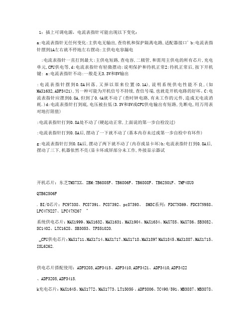
1:插上可调电源,电流表指针可能出现以下变化:a:电流表指针无任何变化:主供电无输出,查待机和保护隔离电路,适配器接口' b:电流表指针摆到1A左右就不停地左右摆动:主供电电容漏电:电流表指针一直打到最大:主供电短路,查电容,二极管,和需用主供电的所有芯片,充电单元,CPU供电等,d:电流表指针有轻微摆动:说明保护和待机正常2:待机正常后,按下开机键: a:电流表指针不动:一般是无3.3V和5V输出:电流表指针摆到0.8A回落,又掉以原来位置(0.1A),说明系统供电性能不良,(如MAX1632,ADP3421),另一种可能为开机信号不持续,查信号端,也就是开机电路的好坏。
C:电流表指针应摆到0.8A,但到了0.4A就不动了(查时钟电路,有未工作的元件,造成无电流消耗.)d:电流表指针打到底,电压被拉低(3.3V和5V或CPU供电输出有短路,先断电,用万用表对地打阻值):电流表指针打到0.8A处不动了(硬起动正常,上面说的第一步自检没过):电流表指针打到0.8A后,摆动了一下就不动了(基本内存未过或第一步自检中有坏件)g:电流表指针打到0.8A后,摆动了两下就不动了(内存或显卡坏)h:电流表指针打到0.8A后,摆动了三下,机器依然不亮(显卡坏或屏部分未工作,外接显示器试开机芯片:东芝TM87XX、IBM:TB6805F、TB6806F、TB6808F、TB62501F、TMP48U0QTB62506F. BI/O芯片:PC97338、PC87391、PC87392、pc87393、 SMSC系列:FDC7N869、FDC37N958、LPC47N227、LPC47N267 ^系统供电芯片:MAX1999、MAX1632、MAX1631、MAX1904、MAX1634、MAX785、MAX786、SB3052、SC1402、LTC1628、SB3053、TPS51020._CPU供电芯片:MAX1711、MAX1714、MAX1717、MAX1718、MAX1897 MAX1845、MAX1887、MAX1715、ISL6262.供电芯片搭配使用:ADP3203,ADP3415、ADP3410,ADP3421、ADP3410,ADP3422、ADP3205,ADP3415.k充电芯片:MAX1645、MAX1772、MAX1773、LT1505G 、ADP3806、TC490/591、MB3887、MB3878、MAX1908 、MAX745、MAX8725.7' WCPU温度控制芯片:MAX1617、AD1020A、AD1030A、CM8500 、MAX1989) c& M7 u% B( m5 c, KG767、ATTM01G、ATTM02G.1显卡品牌:ATI、NVIDIA、S3、NEOMAGIC、TRIDENT、SMI、INTEL、FW82807和CH7001AR搭配使用网卡芯片:RTL8100、RTL8139、Intel DA82562、RC82540、3COM、BCM440Broadcom.c网卡隔离:LF8423、LF-H80P、H-0023、H0024、H0019、ATPL-1192d声卡芯片:ESS1921、ESS1980S、STAC9704、AU8810、4299-JQ、TPA0202、4297-JQ、8552TS、8542TS、CS4239-KQ、BA7786、AD1981B、AN12942 、ALC655., k声卡功放芯片:ESS1980S、G1420、AU8810、TPA0202、TPA0302、TPA03128552TS、8542TS、BA7786、BH7884、ANI2942.,PC卡芯片:R5C551、R5C552、R5C476、R5C472 、R5C593、R5C554、CB1410.oPC卡供电芯片:TPS2204、TPS2205、TPS2206、TPS2216、TPS2211、PU2211、M2562A、M2563A、M2564A 、CP2211、G576COM口芯片:MAX3243、MAX213、ADM213、HIN213、SP3243、MC145583% 键盘芯片:M38857、M38867、M38869、KB3886、7 }:键盘芯片:具有开机功能/images/smilies/default/tongue.gifC87570、PC87591、PC87593、IT8510、pc87541H8系列:、H8/3434、H8/3437、H8/2146、H8/2147、H8/2149、H8/2161、H82169、2 F94 c) L% h' T+ u ?2 ZAAT3200低压差稳压器 -IAAI3680笔记本电脑充电控制芯片AAT4280端口限流保护芯片GAD1885主板声卡芯片 (ADl888主板声卡芯片yADl981主板声卡芯片 3ADP3160,ADP3167笔记本电脑供电控制芯片ADP3166主板CPU供电控制芯片ADP3168笔记本电脑供电控制芯片)& oADP3180主板CPU供电控制芯片eADP3181笔记本电脑CPU供电芯片vADP3203笔记本电脑CPU供电芯片 )ADP3421笔记本电脑CPU供电芯片.eADP3806笔记本电脑电池充,放电控制芯片 !AIC1567主板CPU供电控制芯片 * ~7 C4 \' p: p1 ^! vALC200主板声卡芯片 % l- B7 n o) D! c1 V7 A( nALC201A主板声卡芯片 6 _' O; m$ Z1 K5 B ~+ OALC655主板声卡芯片! w( _AMS1505低压差稳压器eAPA2020,TPA0202小功率音频功率放大芯片[APW7060主板供电控制芯片BQ2040笔记本电脑电池电量检测芯片 . I5 ]9 X4 m6 g7 `1 ? L) ] BQ2060笔记本电脑电池电量检测芯片IBQ24700笔记本电脑充电控制芯片sBQ2470l笔记本电脑充电控制芯片\BQ24702,BQ24703笔记本电脑充电控制芯片CM8501,CM8501A主板内存供电控制芯片# iCM8562主板内存供电控制芯片, [; qCMl9738主板声卡芯片 0 ^8 I, b, q) `; r9 Z: |: o; VCS5322主板CPU供电控制芯片bCS950502主板时钟芯片 2 R/ J6 M+ S" s2 W1 t- Z2 Z. aCY28404C主板时钟芯片~DS1620笔记本电脑数字温度控制芯片) QDS2770笔记本电脑充电控制芯片FAN5056主板CPU供电控制芯片 1 P1 c7 g* f9 P8 j. l8 t3 PFAN7601笔记本电脑电源适配器控制芯片IPM6220A笔记本电脑电源管理芯片 " m ~( ]- J5 I( |+ T, m8 W2 j ISL6223笔记本电脑CPU供电控制芯片( GISL6224笔记本电脑内存供电控制芯片 , Y, |; p! y* aISL6225笔记本电脑内存供电控制芯片 ) Q0 p8 s5 z- o- D: r' ]W$ WLM4861小功率音频功率放大芯片 ; r4 c! i6 p4 a6 z7 P8 \" F LM4863小功率音频功率放大芯片FLM4880几M4881小功率音频功率放大芯片T" DLM4911小功率音频功率放大芯片`LTl505笔记本电脑充电控制芯片/ L7 pLTCl628笔记本电脑系统供电电路 1 @# [# X7 w% ?3 k& D7 U( ILTC1709笔记本电脑CPU供电控制芯片qLTC3728L笔记本电脑系统供电控制芯片W( LLTC4008笔记本电脑充电控制芯片 $ V4 B) @3 G/ J* {_M51995A笔记本电脑电源适配器控制芯片 * x% p. O3 U k! n0 \M61040FP笔记本电脑电池管理控制芯片 7 s( z% R- j# Q5 g0 q% p( gMAXl522,MAXl523,MAXl524笔记本电脑LCD背光电源控制芯片MAX1631笔记本电脑主电源控制芯片?MAXl644笔记本电脑供电控制芯片 ( v& W3 E) X! Q4 J; |) ?MAXl645B笔记本电脑电池充电管理芯片X( KMAX1710,MAX1711,MAXl712笔记本电脑CPU内核供电芯片& jMAX1714笔记本电脑CPU外核供电控制芯片[( MMAX1715笔记本电脑CPU供电芯片~. PMAX1717笔记本电脑CPU供电控制芯片YMAX1718笔记本电脑CPU供电控制芯片 cMAX1736笔记本电脑充电控制芯片. 2 w! MAX1772笔记本电脑充电控制芯片 ; {. L1 @3 a* \' s5 q& ~7 Q5 D$ V' eMAX1773笔记本电脑充电控制芯片_MAX1830,MAXl831笔记本电脑CPU供电控制芯片JMAX1845笔记本电脑CPU内核供电控制芯片 ! o% c3 H1 a" Q3 `1 f* O( JMAX1873笔记本电脑充电控制芯片NMAX1902笔记本电脑系统供电控制芯片 ) }. A p. o7 r$ d, nMAX1908笔记本电脑充电控制芯片 9 J1 o5 h5 O# g |6 eMAX1909笔记本电脑充电控制芯片 & t( z( q+ m, a& v# j6 W+ BXMAX1992,MAXl993笔记本电脑供电控制芯片 / n2 `2 a9 Q/ ]* H4 ^2 vMAX1999笔记本电脑系统供电控制芯片 8 r6 e; C! s8 D. y, ?MAX745笔记本电脑充电控制器 ; `$ m0 c% f# T" cMAX785,MAX786笔记本电脑系统供电控制芯片QMAX8794笔记本电脑DDR内存供电控制芯片UMB3878笔记本电脑充电控制芯片 : ]5 y* k, b6 A+ O1 |MIC2545端口限流保护芯片 1 b# c7 M5 @2 lMIC5205低压差稳压器NCPl205笔记本电脑电源适配器控制芯片4 C7 D" E7 D$ x: ?NCP1207笔记本电脑电源适配器控制芯片 0 q" ^" ~/ Y3 ]$ v" F NCP5201主板DDR2内存供电控制芯片/ {/ o e8 j: \' j6 B* Z B" H" ZNCP5314主板CPU供电控制芯片 ) T9 n6 l+ ?2 @7 WOZ960笔记本电脑液晶屏高压驱动控制芯片\SC1470笔记本电脑供电控制芯片 1 L5 M2 v9 r- R- R, RSC1486,SCl486A笔记本电脑内存供电芯片 0 ?: m5 G1 N) [, t d2 T! hTSC2422主板CPU供电控制芯片\3 hTPS51020笔记本电脑DDR内存供电控制芯片}TPS54672笔记本电脑内存供电控制芯片 6 [) e1 {& q# {; Q7 {) wq特殊芯片:光驱解码芯片、{MICRO OZ168T 0319A MG5PM}h1394接口芯片、{7SB43AB22}一、笔记本不充电(充电芯片损坏) / g: F0 A- ]' Y) w/ n有些笔记本主板维修,突然不能充电,即使拔掉电源,拿出电池,也不能充电,那么这只有一种可能,笔记本充电芯片损坏。
TI BQ IC简介 (Gas Gauge IC)

(電量監測芯片及類比前端保護芯片雖然能提供電壓過載保護, 但它們仍需要透過取樣才能監控電壓,使整個鋰電池保護系統 的反應時間會受到限制,因此需要反應快速、即時和獨立的二
段保護芯片與電量監測芯片及類比前端保護芯片一起工作。)
CONFIDENTIAL
PROSPECT TECHNOLOGY CORP 8
CONFIDENTIAL
PROSPECT TECHNOLOGY CORP 16
TI Gas Gauge IC 頂端標記
Device: bq20Z90 (IT 2nd Gen. Gas Gauge IC) 30-pin TSSOP(DBT) 引腳/封裝 Level-2-260C-1 YEAR(潮濕敏感度等級/回流焊溫度) YMS(89K) : 2008年9月在馬來西亞封裝 (1=Jan, 2=Feb, 3=Mar, 4=Apr, 5=May, 6=Jun, 7=Jul, 8=Aug, 9=Sept, A=Oct, B=Nov, C=Dec) 封裝地點: T: 台灣 W: 菲律賓 K: 馬來西亞 J : 日本 G4: TI 器件/封裝組合轉換成“環保”複合成型 材料的標記. LLLL(FL2K): 追蹤碼(LTC)
CONFIDENTIAL
PROSPECT TECHNOLOGY CORP 17
TI Gas Gauge IC 頂端標記
Device: bq20Z75 (IT 2nd Gen. Gas Gauge IC, bq20z70 +bq29330) 38-pin TSSOP(DBT) 引腳/封裝 Level-2-260C-1 YEAR(潮濕敏感度等級/回流焊溫度) YMS(88T) : 2008年8月在台灣封裝 (1=Jan, 2=Feb, 3=Mar, 4=Apr, 5=May, 6=Jun, 7=Jul, 8=Aug, 9=Sept, A=Oct, B=Nov, C=Dec) 封裝地點:
用于高端手持设备的低成本充电管理芯片BQ24070应用设计
用于高端手持设备的低成本充电管理芯片BQ24070应用设
计
秦小虎
【期刊名称】《电子产品世界》
【年(卷),期】2008(000)005
【摘要】给出详细的锂电池充电管理芯片13Q24070应用设计.
【总页数】4页(P90-93)
【作者】秦小虎
【作者单位】德州仪器半导体技术(上海)有限公司
【正文语种】中文
【中图分类】TP3
【相关文献】
1.应用于手持设备的显示芯片 [J],
2.可涓流充电的串行实时钟芯片DS1302及应用设计 [J], 王明顺;赵德平
3.可涓流充电的串行实时时钟芯片DS1302及应用设计 [J], 王明顺;吴省
4.用于可充电电池的低成本CCR充电方案 [J], Steve Sheard
5.无线能量传输技术有望用于手持设备充电 [J], Christina;Nickolas
因版权原因,仅展示原文概要,查看原文内容请购买。
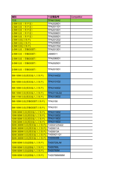
TI Audio芯片选型表
2*40W(BTL),75W(PBTL),带音效处理以及音频算法的DSP,多达3段DRC,动态低音增强:小信 号增强低频信号,大信号压缩的特色,有声场空间拓展3D的音效算法,多段EQ补偿,人声音效,高 保真,THD+N可以做到更小,闭环功放,可使用在大功率的WIFI SPEAKER/Soundbar 2*20W(8欧姆/18V/THD+N=10%),宽电压输入:8V-26V,带MINI DSP,多段EQ调整及2段DRC 2*20W(8欧姆/18V/THD+N=10%),宽电压输入:8V-26V,低音BASS算法,带MINI DSP,多段EQ 调整及2段DRC 2*20W(8欧姆/18V/THD+N=10%),宽电压输入:8V-26V,3D环绕,带MINI DSP,多达16段EQ调 整及2段DRC,最重要还能做2.1(2*SE+BTL),可适用在2.1声道的Soundbar/WIFI SPEAKER/BT SPEAKER 2*30W ,宽电压输入:8V-24V,3D环绕,带MINI DSP,多达16段EQ调整及2段DRC,最重要还能做 2.1(2*SE+BTL),可适用在2.1声道的Soundbar/WIFI SPEAKER/BT SPEAKER 模拟信号转数字信号芯片,通用性强,性价比高,比较适用在对ADC性能要求不高但要求性价比高的应用 TI新推出的主推的高性能ADC,支持MIC麦克风输入,支持最大2vRMS输入,支持差分输入信号, 单电源供电,自动音频信号检测以便降低芯片功耗,软件I2C/SPI控制 硬件控制,支持4Channel,或者2channel差分输入 TI新推出的主推的高性能ADC,高性能,支持4通道 数字信号转模拟信号芯片,性价比高,目前推PCM1754,适用于简单的,客户要求性价比高的音频产品上 TI新推出的高性能DAC,硬件控制,内部集成PLL,最大支持2vRMS输出 可软件控制DAC,可软件自由配置定义一些功能,比较灵活 可差分输出的DAC,封装可以做到更小,集成PLL,无需MCLK,可省外部时钟芯片 4通道DAC,SNR高达118dB,性能高 带EN脚关断使能功能,输入最大6V,输出3.3V,低压差,低静态电流,低功耗,SOT23-5 带EN脚关断使能功能,输入最大6V,输出1.8V,低压差,低静态电流,低功耗,SOT23-5 带EN脚关断使能功能,输入最大5.5V,输出3.3V,低压差,低静态电流,低功耗,SOT23-5 带EN脚关断使能功能,输入最大5.5V,输出1.8V,低压差,低静态电流,低功耗,SOT23-5 输入电压范围为:2.0V-5.5V,输出3.3V,电流800mA,封装为:SOT-223 输入电压范围为2.7-16V,输出3.3V,电流800mA,封装为:SOT-223 输入电压范围为2.7-16V,输出5V,电流800mA,封装为:SOT-223 输入电压范围为2.7-16V,输出可调,电流800mA,封装为:SOT-223 输入电压范围6-42V,输出可调,电流最大可达1A 输入电压范围3.5-28V,输出可调,电流最大可达3A 输入电压范围3.5-28V,输出可调,电流最大可达2A 输入电压范围3.5-42V,输出可调,电流最大可达3.5A 输入电压范围4.5-18V,输出电压范围为0.76-7V,电流输出可达2A 输入电压范围4.5-18V,输出电压范围为0.76-7V,电流输出可达3A 输入4.5V-28V,输出可调,1.7A开关转换器,轻载高效(81%@10mA负载) 输入电压范围4.5V-17V,输出0.76-7V,可调,电流0.5A,封装为:SOT-23,5PIN 输入电压范围4.5V-17V,输出0.76-7V,可调,电流2A,封装为:SOT-23,6PIN 输入电压范围4.5-28V,输出0.8V-25V可调,电流最大可达3A 输入电压范围4.5-17V,输出0.76V-7V可调,电流最大可达3A,封装为:SOT-23,6PIN 输入电压范围4.5-18V,输出0.76V-7V可调,电流最大可达4A,封装为:8-HSOIC 输入电压范围4.5-28V,输出0.8V-25V可调,电流最大可达5A,封装为:8-HSOIC 输入电压范围4.5-18V,输出0.76V-7V可调,电流最大可达6A,封装为:8-HSOIC 输入电压范围为2.97-48V,典型的应用为输出5V/2A,外置MOS
- 1、下载文档前请自行甄别文档内容的完整性,平台不提供额外的编辑、内容补充、找答案等附加服务。
- 2、"仅部分预览"的文档,不可在线预览部分如存在完整性等问题,可反馈申请退款(可完整预览的文档不适用该条件!)。
- 3、如文档侵犯您的权益,请联系客服反馈,我们会尽快为您处理(人工客服工作时间:9:00-18:30)。
bq24072,bq24073bq24074,bq24075,bq24079 SLUS810E–SEPTEMBER2008–REVISED JULY2010 1.5A USB-FRIENDLY Li-Ion BATTERY CHARGER AND POWER-PATH MANAGEMENT ICCheck for Samples:bq24072,bq24073,bq24074,bq24075,bq24079FEATURESDESCRIPTION•Fully Compliant USB Charger–Selectable100mA and500mA Maximum The bq2407x series of devices are integrated Li-ionlinear chargers and system power path management Input Currentdevices targeted at space-limited portable –100mA Maximum Current Limit Ensuresapplications.The devices operate from either a USB Compliance to USB-IF Standardport or AC adapter and support charge currents up to –Input based Dynamic Power Management 1.5A.The input voltage range with input overvoltage (V IN-DPM)for Protection Against Poor USB protection supports unregulated adapters.The USB Sources input current limit accuracy and start up sequenceallow the bq2407x to meet USB-IF inrush current •28V Input Rating with Overvoltage Protectionspecification.Additionally,the input dynamic power •Integrated Dynamic Power Path Management management(VIN-DPM)prevents the charger from (DPPM)Function Simultaneously and crashing incorrectly configured USB sources.Independently Powers the System andThe bq2407x features dynamic power path Charges the Batterymanagement(DPPM)that powers the system while •Supports up to1.5A Charge Current with simultaneously and independently charging the Current Monitoring Output(ISET)battery.The DPPM circuit reduces the charge currentwhen the input current limit causes the system output •Programmable Input Current Limit up to1.5Ato fall to the DPPM threshold;thus,supplying the for Wall Adapterssystem load at all times while monitoring the charge •System Output Tracks Battery Voltagecurrent separately.This feature reduces the number (bq24072)of charge and discharge cycles on the battery,allows •Programmable Termination Current(bq24074)for proper charge termination and enables the systemto run with a defective or absent battery pack.•Battery Disconnect Function with SYSOFFInput(bq24075,bq24079)Typical Application Circuit •Programmable Pre-Charge and Fast-ChargeSafety Timers•Reverse Current,Short-Circuit and ThermalProtection•NTC Thermistor Input•Proprietary Start Up Sequence Limits InrushCurrent•Status Indication–Charging/Done,PowerGood•Small3mm×3mm16Lead QFN PackageAPPLICATIONS•Smart Phones•Portable Media Players•Portable Navigation Devices•Low-Power Handheld DevicesPlease be aware that an important notice concerning availability,standard warranty,and use in critical applications of TexasInstruments semiconductor products and disclaimers thereto appears at the end of this data sheet.Copyright©2008–2010,Texas Instruments Incorporated Products conform to specifications per the terms of the Texasbq24072,bq24073bq24074,bq24075,bq24079SLUS810E–SEPTEMBER2008–REVISED This integrated circuit can be damaged by ESD.Texas Instruments recommends that all integrated circuits be handled with appropriate precautions.Failure to observe proper handling and installation procedures can cause damage.ESD damage can range from subtle performance degradation to complete device failure.Precision integrated circuits may be more susceptible to damage because very small parametric changes could cause the device not to meet its published specifications.DESCRIPTION(CONTINUED)Additionally,the regulated system input enables instant system turn-on when plugged in even with a totally discharged battery.The power-path management architecture also permits the battery to supplement the system current requirements when the adapter cannot deliver the peak system currents,enabling the use of a smaller adapter.The battery is charged in three phases:conditioning,constant current,and constant voltage.In all charge phases,an internal control loop monitors the IC junction temperature and reduces the charge current if the internal temperature threshold is exceeded.The charger power stage and charge current sense functions are fully integrated.The charger function has high accuracy current and voltage regulation loops,charge status display,and charge termination.The input current limit and charge current are programmable using external resistors.ORDERING INFORMATIONPART NUMBER OPTIONALV OVP V BAT(REG)V OUT(REG)V DPPM MARKING(1)(2)FUNCTIONbq24072RGTR 6.6V 4.2V V BAT+225mV V O(REG)–100mV TD CKP bq24072RGTT 6.6V 4.2V V BAT+225mV V O(REG)–100mV TD CKP bq24073RGTR 6.6V 4.2V 4.4V V O(REG)–100mV TD CKQ bq24073RGTT 6.6V 4.2V 4.4V V O(REG)–100mV TD CKQ bq24074RGTR10.5V 4.2V 4.4V V O(REG)–100mV ITERM BZF bq24074RGTT10.5V 4.2V 4.4V V O(REG)–100mV ITERM BZF bq24075RGTR 6.6V 4.2V 5.5V 4.3V SYSOFF CDU bq24075RGTT 6.6V 4.2V 5.5V 4.3V SYSOFF CDU bq24079RGTR 6.6V 4.1V 5.5V 4.3V SYSOFF ODI bq24079RGTT 6.6V 4.1V 5.5V 4.3V SYSOFF ODI(1)The RGT package is available in the following options:R-taped and reeled in quantities of3,000devices per reel.T-taped and reeled in quantities of250devices per reel.(2)This product is RoHS compatible,including a lead concentration that does not exceed0.1%of total product weight,and is suitable foruse in specified lead-free soldering processes.In addition,this product uses package materials that do not contain halogens,including bromine(Br)or antimony(Sb)above0.1%of total product weight.2Submit Documentation Feedback Copyright©2008–2010,Texas Instruments Incorporatedbq24072,bq24073bq24074,bq24075,bq24079 SLUS810E–SEPTEMBER2008–REVISED JULY2010 ABSOLUTE MAXIMUM RATINGS(1)over the0°C to125°C operating free-air temperature range(unless otherwise noted)VALUE UNITIN(with respect to VSS)–0.3to28VBAT(with respect to VSS)–0.3to5VV I Input VoltageOUT,EN1,EN2,CE,TS,ISET,PGOOD,CHG,ILIM,TMR,ITERM,–0.3to7VSYSOFF,TD(with respect to VSS)I I Input Current IN 1.6AOUT5A Output CurrentI O BAT(Discharge mode)5A(Continuous)BAT(Charging mode) 1.5(2)A Output Sink Current CHG,PGOOD15mAT J Junction temperature–40to150°CT stg Storage temperature–65to150°C (1)Stresses beyond those listed under absolute maximum ratings may cause permanent damage to the device.These are stress ratingsonly,and functional operation of the device at these or any other conditions beyond those indicated under recommended operating conditions is not implied.Exposure to absolute-maximum-rated conditions for extended periods may affect device reliability.All voltage values are with respect to the network ground terminal unless otherwise noted.(2)The IC operational charging life is reduced to20,000hours,when charging at1.5A and125°C.The thermal regulation feature reducescharge current if the IC’s junction temperature reaches125°C;thus without a good thermal design the maximum programmed charge current may not be reached.DISSIPATION RATINGSPOWER RATING PACKAGE(1)R q JA R q JCT A≤25°C T A=85°C RGT(2)39.47°C/W 2.4°C/W 2.3W225mW(1)For the most current package and ordering information,see the Package Option Addendum at the end of this document,or see the TIwebsite at .(2)This data is based on using the JEDEC High-K board and the exposed die pad is connected to a Cu pad on the board.The pad isconnected to the ground plane by a2x3via matrix.RECOMMENDED OPERATING CONDITIONSMIN MAX UNIT IN voltage range 4.3526VV I’72,’73,‘75,'79 4.35 6.4 IN operating voltage range V‘74 4.3510.2I IN Input current,IN pin 1.5AI OUT Current,OUT pin 4.5AI BAT Current,BAT pin(Discharging) 4.5AI CHG Current,BAT pin(Charging) 1.5(1)AT J Junction Temperature–40125°CR ILIM Maximum input current programming resistor11008000ΩR ISET Fast-charge current programming resistor(2)5903000ΩR ITERM Termination current programming resistor015kΩR TMR Timer programming resistor1872kΩ(1)The IC operational charging life is reduced to20,000hours,when charging at1.5A and125°C.The thermal regulation feature reducescharge current if the IC’s junction temperature reaches125°C;thus without a good thermal design the maximum programmed charge current may not be reached.(2)Use a1%tolerance resistor for R ISET to avoid issues with the R ISET short test when using the maximum charge current setting. Copyright©2008–2010,Texas Instruments Incorporated Submit Documentation Feedback3bq24072,bq24073bq24074,bq24075,bq24079SLUS810E–SEPTEMBER2008–REVISED ELECTRICAL CHARACTERISTICSOver junction temperature range(0°≤T J≤125°C)and the recommended supply voltage range(unless otherwise noted) PARAMETER TEST CONDITIONS MIN TYP MAX UNIT INPUTUVLO Undervoltage lock-out V IN:0V→4V 3.2 3.3 3.4VV hys Hysteresis on UVLO V IN:4V→0V200300mVInput power detected when V IN>V BAT+V IN(DT)V IN(DT)Input power detection threshold5580130mVV BAT=3.6V,VIN:3.5V→4VV hys Hysteresis on V IN(DT)V BAT=3.6V,V IN:4V→3.5V20mVTime measured from V IN:0V→5V1m st DGL(PGOOD)Deglitch time,input power detected status 1.2msrise-time to PGOOD=LOV IN:5V→7V(’72,’73,’75,'79) 6.4 6.6 6.8V OVP Input overvoltage protection threshold VV IN:5V→11V(’74)10.210.510.8V IN:7V→5V(’72,’73,’75,'79)110V hys Hysteresis on OVP mVV IN:11V→5V(’74)175t DGL(OVP)Input overvoltage blanking time(OVP fault deglitch)50m sTime measured from V IN:11V→5V with1m st REC Input overvoltage recovery time 1.2msfall-time to PGOOD=LOILIM,ISET SHORT CIRCUIT DETECTION(CHECKED DURING STARTUP)I SC Current source V IN>UVLO and V IN>V BAT+V IN(DT) 1.3mAV SC V IN>UVLO and V IN>V BAT+V IN(DT)520mV QUIESCENT CURRENTCE=LO or HI,input power not detected,I BAT(PDWN)Sleep current into BAT pin 6.5m ANo load on OUT pin,T J=85°CEN1=HI,EN2=HI,V IN=6V,T J=85°C50I IN Standby current into IN pin m AEN1=HI,EN2=HI,V IN=10V,T J=85°C200CE=LO,V IN=6V,no load on OUT pin,I CC Active supply current,IN pin 1.5mAV BAT>V BAT(REG),(EN1,EN2)≠(HI,HI)POWER PATHV DO(IN-OUT)V IN–V OUT V IN=4.3V,I IN=1A,V BAT=4.2V300475mVV DO(BAT-OUT)V BAT–V OUT I OUT=1A,V IN=0V,V BAT>3V50100mVV IN>V OUT+V DO(IN-OUT),V BAT<3.2V 3.3 3.4 3.5OUT pin voltage regulation(bq24072)VBAT +V BAT+V BAT+V IN>V OUT+V DO(IN-OUT),V BAT≥3.2V150mV225mV270mVV O(REG)V OUT pin voltage regulation(bq24073,bq24074)V IN>V OUT+V DO(IN-OUT) 4.3 4.4 4.5OUT pin voltage regulation(bq24075,bq24079)V IN>V OUT+V DO(IN-OUT) 5.4 5.5 5.6EN1=LO,EN2=LO9095100mAI IN max Maximum input current EN1=HI,EN2=LO450475500EN2=HI,EN1=LO K ILIM/R ILIM AI LIM=500mA to1.5A150016101720K ILIM Maximum input current factor AΩI LIM=200mA to500mA133015251720I IN max Programmable input current limit range EN2=HI,EN1=LO,R ILIM=8kΩto1.1kΩ2001500mAInput voltage threshold when input current isV IN-DPM EN2=LO,EN1=X 4.35 4.5 4.63V reducedV O(REG)–V O(REG)–V O(REG)–(’72,’73,’74)V Output voltage threshold when charging current is180mV100mV30mVV DPPMreduced(’75,'79) 4.2 4.3 4.4VV OUT≤V BATV BSUP1Enter battery supplement mode V BAT=3.6V,R ILIM=1.5kΩ,R LOAD=10Ω→2ΩV–40mVV OUT≥V BSUP2Exit battery supplement mode V BAT=3.6V,R ILIM=1.5kΩ,R LOAD=2Ω→10ΩVV BAT–20mVV O(SC1)Output short-circuit detection threshold,power-on V IN>V UVLO and V IN>V BAT+V IN(DT)0.80.91VOutput short-circuit detection threshold,supplementV O(SC2)V IN>V UVLO and V IN>V BAT+V IN(DT)200250300mV mode V BAT–V OUT>V O(SC2)indicates short-circuitt DGL(SC2)Deglitch time,supplement mode short circuit250m st REC(SC2)Recovery time,supplement mode short circuit60ms4Submit Documentation Feedback Copyright©2008–2010,Texas Instruments Incorporatedbq24072,bq24073bq24074,bq24075,bq24079 SLUS810E–SEPTEMBER2008–REVISED JULY2010 ELECTRICAL CHARACTERISTICS(continued)Over junction temperature range(0°≤T J≤125°C)and the recommended supply voltage range(unless otherwise noted) PARAMETER TEST CONDITIONS MIN TYP MAX UNIT BATTERY CHARGERI BAT Source current for BAT pin short-circuit detection V BAT=1.5V47.511mAV BAT(SC)BAT pin short-circuit detection threshold V BAT rising 1.6 1.82V('72,'73,'74,'75) 4.16 4.20 4.23V BAT(REG)Battery charge voltage V('79) 4.059 4.100 4.141V LOWV Pre-charge to fast-charge transition threshold V IN>V UVLO and V IN>V BAT+V IN(DT) 2.93 3.1Vt DGL1(LOWV)Deglitch time on pre-charge to fast-charge transition25mst DGL2(LOWV)Deglitch time on fast-charge to pre-charge transition25msV BAT(REG)>V BAT>V LOWV,V IN=5V CE=LO,Battery fast charge current range3001500mAEN1=LO,EN2=HII CHG CE=LO,EN1=LO,EN2=HI,Battery fast charge current V BAT>V LOWV,V IN=5V,I IN max>I CHG,no load on OUT pin,K ISET/R ISET Athermal loop and DPPM loop not activeK ISET Fast charge current factor797890975AΩI PRECHG Pre-charge current K PRECHG/R ISET AK PRECHG Pre-charge current factor7088106AΩCE=LO,(EN1,EN2)≠(LO,LO),0.09×I CHG0.1×I CHG0.11×I CHGV BAT>V RCH,t<t MAXCH,V IN=5V,DPPM loop and thermalloop not activeTermination comparator detection thresholdI TERM A(internally set)CE=LO,(EN1,EN2)=(LO,LO),0.027×I CHG0.033×I CHG0.040×I CHGV BAT>V RCH,t<t MAXCH,V IN=5V,DPPM loop and thermalloop not activeI BIAS(ITERM)Current for external termination-setting resistor V IN>V UVLO and V IN>V BAT+V IN(DT)727578m ATermination current threshold(externally set)I TERM K ITERM×R ITERM/R ISET A(bq24074)USB500or ISET mode(EN1,EN2)≠(LO,LO)0.02250.03000.0375CE=LO,V BAT>V RCH,t<t MAXCH,V IN=5V,DPPM loop andthermal loop not activeK Factor for termination detection thresholdK ITERM A (externally set)(bq24074)USB100mode(EN1,EN2)=(LO,LO),0.0080.01000.012CE=LO,V BAT>V RCH,t<t MAXCH,V IN=5V,DPPM loop andthermal loop not activet DGL(TERM)Deglitch time,termination detected25msV BAT(REG)V BAT(REG)V BAT(REG)V RCH Recharge detection threshold V IN>V UVLO and V IN>V BAT+V IN(DT)V–140mV–100mV–60mVt DGL(RCH)Deglitch time,recharge threshold detected62.5msV BAT=3.6V.Time measured fromt DGL(NO-IN)Delay time,input power loss to OUT LDO turn-off20msV IN:5V→3V1m s fall-timeI BAT(DET)Sink current for battery detection V BAT=2.5V57.510mAt DET Battery detection timer BAT high or low250ms BATTERY CHARGING TIMERSt PRECHG Pre-charge safety timer value TMR=floating144018002160st MAXCHG Charge safety timer value TMR=floating144001800021600st PRECHG Pre-charge safety timer value18kΩ<R TMR<72kΩR TMR×K TMR st MAXCHG Charge safety timer value18kΩ<R TMR<72kΩ10×R TMR×K TMR sK TMR Timer factor364860s/kΩBATTERY-PACK NTC MONITOR(1)I NTC NTC bias current V IN>UVLO and V IN>V BAT+V IN(DT)727578m AV HOT High temperature trip point Battery charging,V TS Falling270300330mVV HYS(HOT)Hysteresis on high trip point Battery charging,V TS Rising from V HOT30mVV COLD Low temperature trip point Battery charging,V TS Rising200021002200mVV HYS(COLD)Hysteresis on low trip point Battery charging,V TS Falling from V COLD300mVt DGL(TS)Deglitch time,pack temperature fault detection TS fault detected to charger disable50msV DIS(TS)TS function disable threshold(bq24072,bq24073)TS unconnected V IN-200mV V THERMAL REGULATIONT J(REG)Temperature regulation limit125°CT J(OFF)Thermal shutdown temperature T J Rising155°CT J(OFF-HYS)Thermal shutdown hysteresis20°C (1)These numbers set trip points of0°C and50°C while charging,with3°C hysteresis on the trip points,with a Vishay Type2curve NTCwith an R25of10kΩ.Copyright©2008–2010,Texas Instruments Incorporated Submit Documentation Feedback5E T RE T E R M R S OF F E T R bq24072,bq24073bq24074,bq24075,bq24079SLUS810E –SEPTEMBER 2008–REVISED JULY 2010ELECTRICAL CHARACTERISTICS (continued)Over junction temperature range (0°≤T J ≤125°C)and the recommended supply voltage range (unless otherwise noted)PARAMETERTEST CONDITIONSMINTYPMAXUNITLOGIC LEVELS ON EN1,EN2,CE,SYSOFF,TD V IL Logic LOW input voltage 00.4V V IH Logic HIGH input voltage 1.46V I IL Input sink current V IL =0V 1m A I IHInput source currentV IH =1.4V10m ALOGIC LEVELS ON PGOOD,CHG V OLOutput LOW voltageI SINK =5mA0.4VRGT PACKAGE (Top View)PIN FUNCTIONSPINNO.I/ODESCRIPTIONNAME'72,'73'74'75,'79External NTC Thermistor Input.Connect the TS input to the NTC thermistor in the battery pack.TS monitors TS 111I a 10k ΩNTC thermistor.For applications that do not utilize the TS function,connect a 10k Ωfixed resistor from TS to VSS to maintain a valid voltage level on TS.Charger Power Stage Output and Battery Voltage Sense Input.Connect BAT to the positive terminal of the BAT2,32,32,3I/Obattery.Bypass BAT to VSS with a 4.7m F to 47m F ceramic capacitor.Charge Enable Active-Low Input.Connect CE to a high logic level to place the battery charger in standby mode.In standby mode,OUT is active and battery supplement mode is still available.Connect CE to a low CE 444I logic level to enable the battery charger.CE is internally pulled down with ~285k Ω.Do not leave CE unconnected to ensure proper operation.EN2555I Input Current Limit Configuration e EN1and EN2control the maximum input current and enable USB compliance.See Table 2for the description of the operation states.EN1and EN2are internally pulled EN1666I down with ≉285k Ω.Do not leave EN1or EN2unconnected to ensure proper operation.Open-drain Power Good Status Indication Output.PGOOD pulls to VSS when a valid input source isPGOOD 777O detected.PGOOD is high-impedance when the input power is not within specified limits.Connect PGOOD to the desired logic voltage rail using a 1k Ω-100k Ωresistor,or use with an LED for visual indication.VSS 888–Ground.Connect to the thermal pad and to the ground rail of the circuit.Open-Drain Charging Status Indication Output.CHG pulls to VSS when the battery is charging.CHG is high CHG999Oimpedance when charging is complete and when charger is disabled.Connect CHG to the desired logic voltage rail using a 1k Ω-100k Ωresistor,or use with an LED for visual indication.System Supply Output.OUT provides a regulated output when the input is below the OVP threshold and above the regulation voltage.When the input is out of the operation range,OUT is connected to V BAT except OUT 10,1110,1110,11Owhen SYSOFF is high (bq24075and bq24079only).Connect OUT to the system load.Bypass OUT to VSS with a 4.7m F to 47m F ceramic capacitor.Adjustable Current Limit Programming Input.Connect a 1100Ωto 8k Ωresistor from ILIM to VSS to program ILIM 121212Ithe maximum input current (EN2=1,EN1=0).The input current includes the system load and the battery charge current.Leaving ILIM unconnected disables all charging.Input Power Connection.Connect IN to the external DC supply (AC adapter or USB port).The input operating range is 4.35V to 6.6V (bq24072,bq24073,bq24075,and bq24079)or 4.35V to 10.5V (bq23074).The input IN 131313Ican accept voltages up to 26V without damage but operation is suspended.Connect bypass capacitor 1m F to 10m F to VSS.6Submit Documentation FeedbackCopyright ©2008–2010,Texas Instruments Incorporatedbq24072,bq24073bq24074,bq24075,bq24079 SLUS810E–SEPTEMBER2008–REVISED JULY2010PIN FUNCTIONS(continued)PINNO.I/O DESCRIPTIONNAME'72,'73'74'75,'79Timer Programming Input.TMR controls the pre-charge and fast-charge safety timers.Connect TMR to VSS TMR141414I to disable all safety timers.Connect a18kΩto72kΩresistor between TMR and VSS to program the timersa desired length.Leave TMR unconnected to set the timers to the default values.Termination Disable Input.Connect TD high to disable charger termination.Connect TD to VSS to enablecharger termination.TD is checked during startup only and cannot be changed during operation.See the TD TD15––Isection in this datasheet for a description of the behavior when termination is disabled.TD is internally pulleddown to VSS with~285kΩ.Do not leave TD unconnected to ensure proper operation.Termination Current Programming Input.Connect a0Ωto15kΩresistor from ITERM to VSS to program the ITERM–15–I termination current.Leave ITERM unconnected to set the termination current to the default10%terminationthreshold.System Enable Input.Connect SYSOFF high to turn off the FET connecting the battery to the system output.When an adapter is connected,charging is also disabled.Connect SYSOFF low for normal operation. SYSOFF––15ISYSOFF is internally pulled up to V BAT through a large resistor(~5MΩ).Do not leave SYSOFF unconnectedto ensure proper operation.Fast Charge Current Programming Input.Connect a590Ωto3kΩresistor from ISET to VSS to program thefast charge current level.Charging is disabled if ISET is left unconnected.While charging,the voltage at ISET ISET161616I/Oreflects the actual charging current and can be used to monitor charge current.See the CHARGE CURRENTTRANSLATOR section for more details.There is an internal electrical connection between the exposed thermal pad and the VSS pin of the device. Thermal The thermal pad must be connected to the same potential as the VSS pin on the printed circuit board.Do not–Pad use the thermal pad as the primary ground input for the device.VSS pin must be connected to ground at alltimes.Table1.EN1/EN2SettingsEN2EN1Maximum input current into IN pinB100modeB500mode10Set by an external resistor from ILIM to VSS11Standby(USB suspend mode)Copyright©2008–2010,Texas Instruments Incorporated Submit Documentation Feedback7bq24072,bq24073bq24074,bq24075,bq24079SLUS810E–SEPTEMBER2008–REVISED SIMPLIFIED BLOCK DIAGRAM Array8Submit Documentation Feedback Copyright©2008–2010,Texas Instruments IncorporatedV500 mV/div5 V/divI V 5 V/divVV 500 mA/divV CHGI BAT2 V/divV BAT1A/div5 V/div2 V/div400ms/divA/div5 V/divII V 3.6 VBAT V 3.825 VOUT I OUT I BATV 3.8 VBAT500 mA/div500 mV/div1 ms/divV 4.4 V OUT 1A/divSupplement ModeI OUTI BAT200 mV/div400s/divm V 4.4 VOUT 500 mA/div500 mA/div5 V/div2 V/div400s/divm 500 mA/divV SYSOFFIBATV 4 VBAT V 5.5 VOUT V CEI BATV 3.6 VBAT V CHG500 mA/div1 V/div5 V/div5 V/div 10 V/div500 mV/div1A/div40s/divm V INI BATV 4.2 VBAT V 4.4 V OUT bq24072,bq24073bq24074,bq24075,bq24079SLUS810E –SEPTEMBER 2008–REVISED JULY 2010TYPICAL CHARACTERISTICSV IN =6V,EN1=1,EN2=0,bq24073application circuit,T A =25°C,unless otherwise noted.ADAPTER PLUG-IN BATTERY CONNECTEDBATTERY DETECTION BATTERY DETECTION R LOAD =10ΩBATTERY INSERTEDBATTERY REMOVEDFigure 1.Figure 2.Figure 3.ENTERING AND EXITING BATTERYENTERING AND EXITING BATTERYSUPPLEMENT MODE SUPPLEMENT MODE ENTERING AND EXITING DPPMMODER LOAD =25ΩTO 4.5ΩR LOAD =20ΩTO 4.5ΩR LOAD =20Ωto 9Ωbq24074bq24072Figure 4.Figure 5.Figure 6.SYSTEM ON/OFF WITH INPUTOVP FAULT CONNECTED V IN =6V to 15V V IN =6VCHARGER ON/OF USING CER LOAD =10Ωbq24075,bq24079Figure 7.Figure 8.Figure 9.Copyright ©2008–2010,Texas Instruments Incorporated Submit Documentation Feedback 9600400100Temperature -Co 3002005000120125130135140145I - m AB A T 5 V/div4 ms/divV I V V255075100T - Junction Temperature - °CJ D r o p o u t V o l t a g e - V -V I N O U T25T - Junction Temperature - °CJ D r o p o u t V o l t a g e - V -V B A TO U T2.53 3.544.5V - O u t p u t V o l t a g e - VO V - Battery Voltage - VBAT 0255075100125T - Junction Temperature - °CJ V - O u t p u t V o l t a g e - VO bq24072,bq24073bq24074,bq24075,bq24079SLUS810E –SEPTEMBER 2008–REVISED JULY 2010TYPICAL CHARACTERISTICS (continued)V IN =6V,EN1=1,EN2=0,bq24073application circuit,T A =25°C,unless otherwise noted.SYSTEM ON/OFF WITH INPUT NOTCONNECTED DROPOUT VOLTAGEV IN =0Vvsbq24075,bq24079THERMAL REGULATIONTEMPERATUREFigure 10.Figure 11.Figure 12.DROPOUT VOLTAGEbq24072bq24072vsOUTPUT REGULATION VOLTAGEOUTPUT REGULATION VOLTAGETEMPERATURE vsvsNO INPUT SUPPLYBATTERY VOLTAGETEMPERATUREFigure 13.Figure 14.Figure 15.10Submit Documentation Feedback Copyright ©2008–2010,Texas Instruments Incorporated255075100125T - Junction Temperature - °CJ V - O u t p u t V o l t a g e - VO4.304.334.354.384.404.434.45255075100125T - Junction Temperature - °CJ V - O u t p u t V o l t a g e - VO 4.1804.1854.1904.1954.2004.2054.21051015202530T - Junction Temperature - °CJ V - R e g u l a t i o n V o l t a g e - VB A T5678910V - Input Voltage - VI I - I n p u t C u r r e nt - m AL I M 0255075100125T - Junction Temperature - °CJ V - O u t p u t V o l t a g eT h r e s h o l d - VO V P 0255075100125T - Junction Temperature - °CJ V - O u t p u t V o l t a g e T h r e s h o l d - VO V P V IN =6V,EN1=1,EN2=0,bq24073application circuit,T A =25°C,unless otherwise noted.bq24073/74bq24075,bq24079OUTPUT REGULATION VOLTAGEOUTPUT REGULATION VOLTAGEBAT REGULATION VOLTAGEvsvsvsTEMPERATURETEMPERATURETEMPERATUREFigure 16.Figure 17.Figure 18.bq24072/73/75/79bq24074bq24074OVERVOLTAGE PROTECTIONOVERVOLTAGE PROTECTIONTHRESHOLDTHRESHOLDINPUT CURRENT LIMITvsvsvsTEMPERATURETEMPERATUREINPUT VOLTAGEFigure 19.Figure 20.Figure 21.33.23.43.6 3.844.2I - F a s t C h a r g e C u r r e n t -AB A T V - Battery Voltage - VBAT 33.23.4 3.6 3.844.2I - F a s t C h a r g e C u r r e n t -AB A T V - Battery Voltage - VBAT 959697989910010110210310410522.22.42.62.83I - P r e c h a r g e C u r r e n t -AB A T V - Battery Voltage - VBAT22.2 2.4 2.6 2.83I - P r e c h a r g e C u r r e n t -AB A T V - Battery Voltage - VBAT V IN =6V,EN1=1,EN2=0,bq24073application circuit,T A =25°C,unless otherwise noted.FASTCHARGE CURRENTFASTCHARGE CURRENTPRECHARGE CURRENTvsvsvsBATTERY VOLTAGEBATTERY VOLTAGEBATTERY VOLTAGEFigure 22.Figure 23.Figure 24.PRECHARGE CURRENTvsBATTERY VOLTAGEFigure 25.APPLICATION CIRCUITSV IN=UVLO to V OVP,I FASTCHG=800mA,I IN(MAX)=1.3A,Battery Temperature Charge Range=0°C to50°C,6.25 hour Fastcharge Safety Timering bq24072/bq24073in a Host Controlled Charger ApplicationV IN=UVLO to V OVP,I FASTCHG=800mA,I IN(MAX)= 1.3A,I TERM=110mA,Battery Temperature Charge Range=0°C to50°C,Safety Timers disableding bq24074in a Stand Alone Charger ApplicationV IN=UVLO to V OVP,I FASTCHG=800mA,I IN(MAX)=1.3A,Battery Temperature Charge Range=0°C to50°C, 6.25hour Fastcharge Safety Timering bq24075or bq24079to Disconnect the Battery from the System。