外文翻译 运算放大器的原理和应用
反相运算放大器的应用原理

反相运算放大器的应用原理概述反相运算放大器是一种常见的电子电路元件,广泛应用于模拟电子领域。
本文将介绍反相运算放大器的基本原理和应用。
基本原理反相运算放大器是一种基于运算放大器的电路,在电路中使用了一个运算放大器和几个电阻。
下面是反相运算放大器的基本原理:1.运算放大器:运算放大器(Operational Amplifier,简称Op-Amp)是一种特殊的电子放大器,具有高增益、高输入阻抗和低输出阻抗等特性。
它有两个输入端(正输入端和负输入端)和一个输出端。
2.反向输入:反相运算放大器通过将输入信号接到运算放大器的负输入端(inverting input)来实现反向输入。
3.反馈电阻:反相运算放大器使用反馈电阻(Feedback Resistor)将运算放大器的输出信号反馈到负输入端。
4.放大倍数:通过调整反馈电阻的数值,可以控制运算放大器的放大倍数。
当反馈电阻的阻值较大时,放大倍数也较大。
应用原理反相运算放大器具有很多应用原理,下面将介绍其中几个常见的应用:1. 反相放大器反相放大器是反向输入信号并放大的电路,具有以下特点:•输入信号:将输入信号接到反相运算放大器的正输入端,通过反馈电阻将负输入端与输出端连接。
•放大倍数:反相放大器的放大倍数由反馈电阻和输入电阻决定,计算公式为:放大倍数 = -反馈电阻 / 输入电阻。
•相位反转:由于反向输入,反相放大器会使输入信号相位发生180°的变化,即相位反转。
2. 滤波器利用反相运算放大器的特性,可以设计出各种滤波器电路,如低通滤波器、高通滤波器和带通滤波器等。
•低通滤波器:将低频信号通过而抑制高频信号。
设计方法是选择合适的电容和电阻,使得截止频率符合要求。
•高通滤波器:将高频信号通过而抑制低频信号。
设计方法类似于低通滤波器,只是选取的元件参数不同。
•带通滤波器:能够通过某一范围内的频率信号,并抑制其他频率信号。
可以通过组合低通滤波器和高通滤波器实现。
电路中的运算放大器与比较器的原理与应用

电路中的运算放大器与比较器的原理与应用在电子领域中,运算放大器(Operational Amplifier,简称Op Amp)与比较器(Comparator)是两个非常重要的电子元件。
它们在电路设计与应用中起着至关重要的作用。
一、运算放大器的原理与应用运算放大器是一种具有差分放大功能的电子放大器。
它通常由多个晶体管以及与之相连的电阻、电容等元件组成。
运算放大器的输出信号是其输入信号的放大倍数。
1. 基本原理运算放大器的基本电路结构由一个差分放大器和一个输出级组成。
它有两个输入端,称为非反相输入端(+)和反相输入端(-),以及一个输出端。
其基本工作模式是将输入信号放大,并输出一个与输入信号有相关性的信号。
2. 应用领域运算放大器在电路设计中有广泛的应用,包括:(1)信号放大:将弱信号放大至适当的电平,以便进行后续处理;(2)滤波器设计:根据不同的频率要求,设计低通、高通、带通等类型的滤波器;(3)振荡器设计:用于产生高频信号的振荡器电路设计;(4)比例控制与调节:用于控制系统,在反馈环路中起到稳定系统的作用。
二、比较器的原理与应用比较器是一种电子元件,用于将两个输入进行比较,并输出一个相应的逻辑电平。
它通常由运算放大器、基准电压和一个阈值元件组成。
1. 基本原理比较器的基本原理是将两个输入信号进行比较,并输出一个高、低逻辑电平。
当一个输入信号高于另一个输入信号时,输出为高电平,反之输出为低电平。
2. 应用领域比较器在电子领域中应用广泛,包括:(1)开关控制:将比较器的输出连接到开关控制电路中,根据两个输入信号的大小关系来控制开关的开关与闭合;(2)模拟电压转数字信号:将模拟电压通过比较器进行比较,并将结果输出为数字信号,用于数字电路的处理;(3)电压检测与监测:将比较器连接到电压检测电路中,用于监测输入电压是否超过设定值。
总结起来,运算放大器和比较器是电子领域中非常常见的电子元件,它们在电路设计与应用中功不可没。
运算放大器基本原理及应用
运算放大器基本原理及应用一. 原理(一) 运算放大器1.原理运算放大器是目前应用最广泛的一种器件;当外部接入不同的线性或非线性元器件组成输入和负反馈电路时;可以灵活地实现各种特定的函数关系..在线性应用方面;可组成比例、加法、减法、积分、微分、对数等模拟运算电路..运算放大器一般由4个部分组成;偏置电路;输入级;中间级;输出级..图1运算放大器的特性曲线 图2运算放大器输入输出端图示图1是运算放大器的特性曲线;一般用到的只是曲线中的线性部分..如图2所示..U -对应的端子为“-”;当输入U -单独加于该端子时;输出电压与输入电压U -反相;故称它为反相输入端..U +对应的端子为“+”;当输入U +单独由该端加入时;输出电压与U +同相;故称它为同相输入端..输出:U 0= AU +-U - ; A 称为运算放大器的开环增益开环电压放大倍数.. 在实际运用经常将运放理想化;这是由于一般说来;运放的输入电阻很大;开环增益也很大;输出电阻很小;可以将之视为理想化的;这样就能得到:开环电压增益A ud =∞;输入阻抗r i =∞;输出阻抗r o =0;带宽f BW =∞;失调与漂移均为零等理想化参数..2.理想运放在线性应用时的两个重要特性输出电压U O 与输入电压之间满足关系式:U O =A ud U +-U -;由于A ud =∞;而U O 为有限值;因此;U +-U -≈0..即U +≈U -;称为“虚短”..由于r i =∞;故流进运放两个输入端的电流可视为零;即I IB =0;称为“虚断”;这说明运放对其前级吸取电流极小..上述两个特性是分析理想运放应用电路的基本原则;可简化运放电路的计算.. 3. 运算放大器的应用 1比例电路所谓的比例电路就是将输入信号按比例放大的电路;比例电路又分为反向比例电路、同相比例电路、差动比例电路.. a 反向比例电路反向比例电路如图3所示;输入信号加入反相输入端:图3反向比例电路电路图对于理想运放;该电路的输出电压与输入电压之间的关系为:为了减小输入级偏置电流引起的运算误差;在同相输入端应接入平衡电阻R ’=R 1 // R F ..输出电压U 0与输入电压U i 称比例关系;方向相反;改变比例系数;即改变两个电阻的阻值就可以改变输出电压的值..反向比例电路对于输入信号的负载能力有一定的要求.. b 同向比例电路同向比例电路如图4所示;跟反向比例电路本质上差不多;除了同向接地的一段是反向输入端:图4 同相比例电路电路图它的输出电压与输入电压之间的关系为:; R’=R 1 // R F只要改变比例系数就能改变输出电压;且U i 与U 0的方向相同;同向比例电路对集成运放的共模抑制比要求高.. c 差动比例电路差动比例电路如图5所示;输入信号分别加在反相输入端和同相输入端:图5 差动比例电路电路图其输入和输出的关系为:i1f O U R R U -=i1fO )U R R (1U +=可以看出它实际完成的是:对输入两信号的差运算.. 2和/差电路 a 反相求和电路其电路图如图6所示输入端的个数可根据需要进行调整:图6 反相求和电路图其中电阻R'满足:它的输出电压与输入电压的关系为:它的特点与反相比例电路相同;可以十分方便的通过改变某一电路的输入电阻;来改变电路的比例关系;而不影响其它支路的比例关系.. b 同相求和电路其电路如图7所示输入端的个数可根据需要进行调整:图7 同向求和电路图它的输出电压与输入电压的关系为:它的调节不如反相求和电路;而且它的共模输入信号大;因此它的应用不很广泛.. c 和差电路其电路图如图8所示;此电路的功能是对U i1、U i2进行反相求和;对U i3、U i4进行同相求和;然后进行的叠加即得和差结果..图8 和差电路图它的输入输出电压的关系是:由于该电路用一只集成运放;它的电阻计算和电路调整均不方便;因此我们常用二级集成运放组成和差电路..它的电路图如图9所示:图9 二级集成和差电路图它的输入输出电压的关系是:⎪⎪⎭⎫⎝⎛--+=22114433f 0R U R U R U R U R U i i i i它的后级对前级没有影响采用理想的集成运放;它的计算十分方便.. 3 积分电路和微分电路 a 积分电路其电路图如图10所示:它是利用电容的充放电来实现积分运算;可实现积分运算及产生三角波形等..图10 积分电路图它的输入、输出电压的关系为:其中: 表示电容两端的初始电压值.如果电路输入的电压波形是方形;则产生三角波形输出.. b 微分电路微分是积分的逆运算;它的输出电压与输入电压呈微分关系..电路如图11所示:图11 微分电路图R u -=0它的输入、输出电压的关系为: 4 对数和指数运算电路 a 对数运算电路对数运算电路就是是输出电压与输入电压呈对数函数..我们把反相比例电路中Rf 用二极管或三级管代替级组成了对数运算电路..电路图如图12所示:图12 对数运算电路它的输入、输出电压的关系为也可以用三级管代替二极管: b 指数运算电路指数运算电路是对数运算的逆运算;将指数运算电路的二极管三级管与电阻R 对换即可..电路图如13所示:图13 指数运算电路它的输入、输出电压的关系为: 利用对数和指数运算以及比例;和差运算电路;可组成乘法或除法运算电路和其它非线性运算电路..二无源滤波电路0101=+-=⎰t c t t i u dt u RC u r iu u S I u Re 0-=滤波电路的作用:允许规定范围内的信号通过;而使规定范围之外的信号不能通过..滤波电路的分类:低通滤波器:允许低频率的信号通过;将高频信号衰减; 高通滤波器:允许高频信号通过;将低频信号衰减;带通滤波器:允许一定频带范围内的信号通过;将此频带外的信号衰减; 带阻滤波器:阻止某一频带范围内的信号通过;允许此频带以外的信号衰减;仅由无源元件电阻、电容、电感组成的滤波电路;为无源滤波电路..它有很大的缺陷如:电路小;能力差等..为此我们要学习有源滤波电路.. 三有源滤波电路有源滤波器是指利用放大器、电阻和电容组成的滤波电路;可用在信息处理、数据传输、抑制干扰等方面..但因受运算放大器频带限制;这种滤波器主要用于低频范围..1一阶有源低通滤波器其电路如图14-a 所示;它是由一级RC 低通电路的输出再接上一个同相输入比例放大器构成; 幅频特性如图14-b 所示; 通带以外以dB 20-/十倍频衰减:图14-a 一阶有源低通滤波电路 图14-b 一阶有源低通幅频特性该电路的传递函数为: 式中RC 10=ω称为截止角频率;传递函数的模为2)(1)(o vo v A j A ωωω+=幅角为00arctg ωωϕ-=)(.. 2二阶有源滤波电路为了使输出电压以更快的速率下降;以改善滤波效果;再加一节RC 低通滤波环节;称为二阶有源滤波电路..它比一阶低通滤波器的滤波效果更好..二阶有源滤波器的典型结构如图15所示:图15 二阶有源滤波器典型结构 图中;Y 1~Y 5为导纳;考虑到U P =U N ;可列出相应的节点方程式为: 在节点A 有: 在节点B 有: 联立以上二等式得:考虑到: 则:AS 即是二阶压控电压源滤波器传递函数的一般表达式..只要适当选择Y i i =1~5;就可以构成低通、高通、带通等有源滤波器..)(ba aO N P R R R U U U +=≈。
运算放大器的用法
运算放大器的用法运算放大器(Operational Amplifier,简称Op-Amp)是一种重要的电子器件,广泛应用于各种电路中。
它具有高增益、高输入阻抗、低输出阻抗等特点,使得它在电子设计中扮演着重要的角色。
下面将介绍一些运算放大器的常见用法。
1. 比较器:运算放大器可以用作比较器,将两个输入信号进行比较,并输出一个高电平或低电平的信号。
这种应用常见于电压比较、开关控制等场景。
2. 放大器:运算放大器最常见的用途是作为信号放大器。
通过调整反馈电阻和输入电阻的比例,可以实现不同的放大倍数。
这种应用广泛用于音频放大、传感器信号处理等领域。
3. 滤波器:运算放大器可以与电容和电感等元件组成滤波电路,实现对特定频率范围内信号的增强或抑制。
这种应用常见于音频滤波、通信系统中的滤波等场景。
4. 仪表放大器:运算放大器可以通过调整反馈网络来实现对输入信号进行精确测量和调节。
这种应用常见于仪器仪表、传感器信号调理等领域。
5. 电压跟随器:运算放大器可以实现输入电压与输出电压一致的功能,即输入电压变化时,输出电压也相应变化。
这种应用常见于自动控制系统、反馈控制等场景。
6. 信号发生器:通过在运算放大器的反馈回路中引入RC网络,可以实现正弦波、方波等不同形式的信号发生。
这种应用常见于测试仪器、音频设备等领域。
总之,运算放大器作为一种重要的电子元件,在各个领域都有广泛的应用。
它的高增益、高输入阻抗和低输出阻抗等特点使得它成为了电子设计中不可或缺的工具。
无论是在信号处理、控制系统还是仪表测量等方面,运算放大器都发挥着重要作用,为我们提供了更加精确和稳定的电子系统。
外文翻译--运算放大器的原理和应用
Operational amplifier theory and applications1 the principle of op-ampOp amp is the most widely used of a device, although the different structure of different operational amplifier, but the external circuit, its characteristics are the same. Op amp is usually 4 parts, bias circuits, input stage, intermediate-level, output level, which is generally used input stage differential amplifier circuit (inhibitory power), the middle class in general the use of active load circuit loads the total radio (increase the magnification), the complementary output stage generally symmetrical output stage circuit (drive circuit to increase the capacity of the load), here is a brief introduction about the realization of the specific complex.Industries, an operational amplifier used to measure the performance of many of the indicators, the actual operational amplifier is generally believed that the closer the ideal op amp, the better, the classroom involved, we are only asking the equivalent input resistance of infinity, infinite open-loop gain, In fact, there are many other indicators, I will, are you a brief introduction, the performance of operational amplifiers including the five indicators, open-loop differential-mode voltage amplification factor, the maximum output voltage, differential-mode input resistance, output resistance, common mode rejection ratio CMRR. (Open-loop differential-mode is the magnification on the integrated delivery without additional feedback loop in case of differential-mode voltage amplification. Maximum output voltage is saying that it refers to a certain voltage, the integrated operational amplifier is not the largest output voltage distortion peak - peak. differential-mode input resistance reflects the size of integrated operational amplifier input differential-mode input signal to obtain the current size of the source. requiring the greater the better. reflect the size of the output resistance of an integrated transport on the small-signal output load capacity. CMRR shown on the integrated operational amplifier common-mode rejection of input signals, which is defined with the differential amplifier circuit. CMRR the better.)Figure 1 op-amp characteristic curveFigure 2 op-amp input and output terminal mapFigure 1 is the characteristic curve of amplifier is generally used only the linear part of curve. As shown in Figure 2. U-corresponding to the terminal "-", when the importation of Canadian U-separate from the terminal, the output voltage and input voltage U-RP, the RP-call input. U + corresponding to the terminal "+", when the input U + separate from the client to join, the output voltage and U + with the phase, so called in-phase input.Output: U0 = A (U +-U-); A known as the op amp's open loop gain (open-loop voltage amplification factor)In the practical application of often idealized op amp, this is because generally speaking, the input resistance OPAMP great open-loop gain, output resistance is very small, can be regarded as ideal, it can be : Ri ≈ ∞, Ro ≈ 0, A ≈ ∞. By A ≈ ∞, be U + ≈ U-, a result similar to the two inputs can be seen as a short-circuit (referred to as the "virtual short"), if the input termination in the same direction, the reverse input and almost the same potential (referred to as "virtual land"). By Ri ≈ ∞, we can see thatsimilar to the input circuit is equal to 0, it can be seen as the input circuit (known as the "virtual shutdown").2 Application of Operational AmplifiersHere only the application of the ideal operational amplifier, the actual op amp can be seen as similar to an ideal operational amplifier. Application of operational amplifiers is very broad, here we only talk about the op-amp with some focus on other components of the computing circuit. Application of circuit operation in terms of comparison with other more extensive, and easy to understand some of them. Computing the ratio of the circuit including the circuit, and differential circuit, integro-differential circuit, and the index of the number of computing circuit.1. The proportion of the circuit:The proportion of the so-called circuit is proportional to the input signal amplification circuit, the ratio of the reverse circuit is divided into the proportion of the circuit, the circuit with the phase ratio, the ratio of differential circuit.(1) reverse the ratio of the circuit:Reverse the ratio of the circuit shown in Figure 3, the input signal input by adding RP, there areFigure 3 the ratio of the reverse circuit schematicsFigure 4 with the ratio of circuit schematicsU P =U N =0 I P =I N =0Know from Kirchhoff's law:I R =I F (U I -U N )/R =(U N -U O )/R fU O =I F U RR - Thus know that the output voltage U0 and the ratio of input voltage Ui said therelationship between the opposite direction, changing the ratio of coefficients, namely, two resistors of resistance to change can change the value of output voltage. Reverse the ratio of operational amplifier circuits for the performance of a certain performance requirements, such as the input signal to a certain load capacity requirements..(2) the ratio of the circuit in the same direction (Figure 4):With the reverse ratio of the circuit is essentially similar, apart from a section of ground in the same direction is the reverse input fromU P =U N =U I I R =I F 得:U N /R =(U O -U N )/R fSO: U O =I F U R R )(+1 So as long as the coefficient of change in the proportion of the output voltage can be changed, and U0 and Ui the same direction, of course, with the proportion of the circuit is to have a certain requirements, such as the integrated operational amplifier of the common mode rejection ratio requirements.(3) the ratio of differential circuit (Figure 5):U O =)(121I I F U U R R - Input signal, respectively, added to the RP-phase input and input, the specific steps and not in the first two are derived almostAnd in the end be:From this we can see that it is actually completed: two of the input differential signal operation.2. And the difference circuit:And poor use of the circuit is a relatively wide range of circuits, where the three circuits on the move: Reverse summation circuit to sum the same circuit, and differential circuits.(1) reverse summation circuit and summation circuit in the same direction:Only difference is that the input signal by adding a reversed-phase input with input phase difference, reverse-sum circuit in Figure 6, with the summation circuit in Figure7. By Kirchhoff's current law, reverse summation circuit output voltage and input voltage relationship,U O =)(332211R U R U R U R I I I F ++-Figure 5 the proportion of the circuit differential circuitFigure 6 Reverse summation circuit schematicsFigure 7 with the circuit diagrams and circuitWith the summation circuit output voltage and the relationship between the input voltage as follows:U O =)(321CI B I A I F R U R U R U R ++ Although the comparison between the two similar, but different, the reverse sum of the characteristics of the circuit with the same RP-circuit ratio. It can be veryconvenient for the input resistance of a circuit to change the relationship between the proportion of the circuit without affecting the relationship between the proportion of other routes. And with the application to the summation circuit is not very extensive, mainly because of its better regulation of RP-sum circuit, and its large common-mode input signal.(2) and the difference circuit:Its circuit diagram is shown in Figure 8. The function of this circuit is Ui1, Ui2 carried out by RP-summation of Ui3, Ui4 sum to the same direction, and then superimposed the results obtained and the poor, and his relationship between input and output voltage as follows:U O =)(22114433R U R U R U R U R I I I I F --+Figure 8 and the differential circuit schematicsAs the use of an integrated circuit operational amplifier, and its calculation and the circuit resistance is not easy to adjust, so we used the composition of the secondaryoperational amplifier integrated circuit and poor. Its circuit diagram as shown in Figure 9, it's the relationship between input and output voltage is:U O =)(22114433R U R U R U R U R I I I I F --+Figure 9 composed of two integrated operational amplifier circuit schematics and poorIts former level after the level does not affect (in the ideal of integrated operational amplifier), which is very convenient calculation.3. Integral and differential circuit:The above components used are basically resistive element, if one side of the resistor capacitor replaced, then the results will become integral circuits and differential circuits.(1) integral circuit:The circuit shown in figure 10, it can achieve integration and production of computing, such as triangular waveform. Integral operation is: the output voltage and input voltage relations were integral. It is the use of capacitive charge and discharge operations to achieve integration, and its input and output voltage relationship:U O =dt U RC I ⎰-1 One: that the initial capacitor voltage at both ends. If the circuit input voltage waveform is a square, then have a triangular waveform output.(2) differential circuit:Differential circuits and the difference between circuit points just swap the location of resistors and capacitors. Differential is the integral of the inverse operation, its output voltage and input voltage relations showed differential. Circuit diagram shown in Figure 11: its input and output voltage relationship:U O =I U dt d CR -Circuit schematics Figure 10 pointFigure 11 Differential circuit schematics4. And the index calculation on the number of circuits:Circuit used for a number of diodes, diode characteristics of the most important is one-dimensional conductivity. In the circuit, the current only flows from the diode cathode, anode flow, it is the realization of the characteristics and indicators of the number of circuits.(1) of the number of operation circuits:U O =ri u U s i T ln - Logarithm computing circuit output voltage and input voltage was logarithmicfunction. RP we use the ratio of Rf diode circuit that is formed instead of the number of operations on the circuit. Circuit diagram shown in Figure 12. He relationship between the output of the input voltage isFigure 12 Logarithm computing circuit schematicsFigure 13 Index computation circuit schematicsIn fact, transistor can also be used in place of diodes, the principle is the same, in addition to a multi-line connections.(2) index operation circuits:U O =R e I T iU u SIndex calculation on the number of circuits and circuit computing the difference is only diodes and resistors to each other location, the index is the number of operation circuits computing inverse operation, the index of the diode operation circuits (three tubes) and the resistance R of the exchange can be. Circuit as shown in 13 Its input and output voltage relationshipUse of computing as well as index number and the proportion of poor operation and circuit can be composed of multiplication or division operation circuits and other non-linear operation circuit, will no longer be described here.中文翻译:运算放大器的原理和应用1 运算放大器的原理运算放大器是目前应用最广泛的一种器件,虽然各中不同的运放结构不同,但对于外部电路而言,其特性都是一样的。
运放工作原理
运放工作原理
运放(Operational Amplifier,简称运算放大器)是一种放大电路,是一种典型的双端输入单端输出放大器,它的输出放大程度大于它的输入电压变化量,是一种极为重要的电子元件。
运放的工作原理主要是利用电路中引入的小电压产生的饱和放大效果,当输出电压超过一定的正零阈值的时候放大器就会饱和,从而产生最大的放大倍数。
运放主要包括底片电路和耦合电容电路、补偿电容、恒压稳压器、反馈电路、动态稳定器。
底片电路中应用两个N沟道MOS(N-channel Metal Oxide Semiconductor)产生左右两个源电流,通过晶体管运算放大器会取到较大输出电压;耦合电容电路将输入电压和接地隔离,把输入信号前移到反馈电路;补偿电容元件用于调整反馈电路的相位,把带宽限制在一定的范围内;恒压稳压器类似与电源分离,提供了稳定的电压,确保输入信号准确无误;反馈电路是取信号的行为方面,用来还原输入信号;动态平衡器是针对反馈电路振荡不稳定特性给出的一种补偿线路,它增加了反馈电路的稳定性,避免了放大器的饱和和振荡现象的出现。
底片电路、耦合电容电路、恒压稳压器、反馈电路等参与输入信号的传递,传递出去的输入信号受到了增益的放大,补偿电容元件和动态平衡器起到了稳定放大器的作用,以及同时保证输入信号的准确性、精确度和输出信号的高纯度。
另外,运放还具有低电源噪声、抗输入和输出噪声、良好的品能和可靠性、节能减污等特点,因此在应用领域也得到了广泛的发展。
运放被广泛应用于电路开关、信号传感、信号处理、逻辑控制、精密测量、信号放大等器件的应用,是现今电子技术应用不可或缺的元件之一。
运算放大器的原理及特性
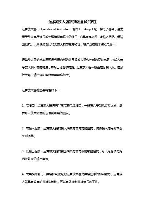
运算放大器的原理及特性
运算放大器(Operational Amplifier,简称Op Amp)是一种电子器件,通常用于放大电压信号或处理模拟电路中的信号。
它具有高增益、高输入阻抗、低输出阻抗、大共模抑制比和无穷大的带宽等特性,被广泛应用于模拟电路中。
运算放大器的基本原理是利用内部的共尺极放大器和外部的反馈电路,将输入信号放大到所需的幅度,并输出给后续电路。
运算放大器一般由差分输入级、差分放大器、输出级和电源供电电路组成。
运算放大器的主要特性如下:
1. 高增益:运算放大器具有非常高的电压增益,一般在几千到几百万之间。
这样可以放大微弱的信号到可用的幅度。
2. 高输入阻抗:运算放大器的输入端具有非常高的阻抗,使得输入信号源不会受到损耗。
3. 低输出阻抗:运算放大器的输出端具有非常低的输出阻抗,可以给后续电路提供较大的输出电流。
4. 大共模抑制比:共模抑制比是指运算放大器对共模信号的抑制能力。
运算放大器具有较高的共模抑制比,可以有效抑制共模信号的干扰。
5. 无穷大的带宽:运算放大器的带宽足够大,可以处理宽频带的信号。
6. 可调节增益:通过调整反馈电阻,可以调节运算放大器的增益。
运算放大器常常用于放大电压信号、求和运算、积分运算、微分运算等,广泛应用于滤波器、放大器、比较器、多路选择器等电路中。
运算放大器电路原理

运算放大器电路原理运算放大器(Operational Amplifier,简称Op-Amp)是一种极为重要的电子元器件,广泛应用于各种电路中。
它具有高增益、差分输入、单端输出等特点,能够放大电压、电流和功率等信号,并提供微弱信号的放大和处理功能。
本文将介绍运算放大器的基本原理及其电路结构。
一、运算放大器的基本原理运算放大器是一个多元件集成电路(IC),通常由几个晶体管、电阻和电容器等元件组成。
它的核心部分是一个差分放大器,具有高增益特性。
运算放大器的输出电压与输入电压之间的关系可以通过下面的公式表示:Vout = Av (V+ - V-)其中,Vout为输出电压,Av为放大器的开环增益,V+和V-分别为非反相输入和反相输入。
二、运算放大器的电路结构运算放大器的电路图可以简化为以下几个主要部分:1.差动放大器:差动放大器是运算放大器的核心部分,它由两个输入电源、两个输入电容和两个晶体管等电路组成。
它的作用是将输入信号进行差分放大,增益高达几千倍。
2.电流镜:电流镜是一个由晶体管组成的电流源,用于提供稳定的电流输出。
它的作用是保持差动放大器的工作点稳定,使得差动放大器的输出可以线性放大。
3.级联放大器:级联放大器由多个差分放大器组成,用于提高整个运算放大器的放大倍数。
每个差分放大器都会放大之前的放大器的输出信号。
4.反馈网络:反馈网络是运算放大器的重要部分,通过它可以实现对输出信号进行控制和调整。
反馈网络可以分为正反馈和负反馈两种形式,具体的选择取决于应用的要求。
三、运算放大器的应用运算放大器在电子电路中具有广泛的应用,主要包括以下几个方面:1.信号放大:运算放大器可将输入信号放大到所需的幅度,用于增强微弱信号。
2.滤波:运算放大器可以配合电容器和电阻等元件,构成滤波电路,用于滤除不需要的频率成分,提取特定频率的信号。
3.比较器:运算放大器可以作为比较器使用,用于判断输入信号的大小关系,并输出相应的逻辑电平。
- 1、下载文档前请自行甄别文档内容的完整性,平台不提供额外的编辑、内容补充、找答案等附加服务。
- 2、"仅部分预览"的文档,不可在线预览部分如存在完整性等问题,可反馈申请退款(可完整预览的文档不适用该条件!)。
- 3、如文档侵犯您的权益,请联系客服反馈,我们会尽快为您处理(人工客服工作时间:9:00-18:30)。
如图 1 是运算放大器的特性曲线,一般用到的只是曲线中的线性部分。如图 2 所示。U-对应的端子为 “-”,当输入 U-单独加于该端子时,输出电压与输入电压 U反相,故称它为反相输入端。U+对应的端子为“+”,当输入 U+单独由该端加入时, 输出电压与 U+同相,故称它为同相输入端。 输出:U0= A(U+-U-) ; A称为运算放大器的开环增益(开环电压放大倍数)
1 运算放大器的原理
虽然各种不同的运放结构不同,但对于外部电路而言,其特性都是一样的。运算 放大器一般由4个部分组成,偏置电路,输入级,中间级,输出级,其中输入级一般 是采用差动放大电路(抑制电源),中间级一般采用有源负载的共射负载电路(提 高放大倍数),输出级一般采用互补对称输出级电路(提高电路驱动负载的能力)。 工业上,用来衡量一个运算放大器的性能的指标有很多,一般认为实际运算放大 器越接近理想运放就越好,课堂上我们涉及到的只是要求输入端等效电阻无穷大, 开环增益无穷大,其实还有很多其他的指标,我就简要介绍下吧,运算放大器的性 能指标包括5个,开环差模电压放大倍数,最大输出电压,差模输入电阻,输出电阻, 共模抑制比CMRR。(开环差模放大倍数是指集成运放在无外加反馈回路的情况下 的差模电压的放大倍数。最大输出电压是指它是指一定电压下,集成运放的最大不 失真输出电压的峰--峰值。 差模输入电阻的大小反映了集成运放输入端向差模输入信 号源索取电流的大小。要求它愈大愈好。输出电阻的大小反映了集成运放在小信号 输出时的负载能力。共模抑制比放映了集成运放对共模输入信号的抑制能力,其定 义同差动放大电路。CMRR越大越好。)
5
极管代替即组成了对数运算电路。电路图如图 12 所示。于是他的输出输入电压关系 是
其实也可以用三极管代替二极管,原理是一样的,除了要多连接一条线路。 (2) 指数运算电路:
U O I S e uT R
ui
指数运算电路与对数运算电路差别仅仅只是把二极管和电阻互相位置,指数运 算电路是对数运算的逆运算,将指数运算电路的二极管(三级管)与电阻R对换即可。 电 路图如图13所示。 利用对数和指数运算以及比例,和差运算电路,可组成乘法或除法运算电路和 其它非线性运算电路,此处就不再介绍了。
UO Rf ( U I 3 U I 4 U I1 U I 2 ) R3 R4 R1 R2
图 8 和差电路电路图
2.3
积分和微分电路: 以上用到的元件基本上都是电阻元件,如果其中端的电阻换成电容,那么结果就
会变成积分电路和微分电路。 (1) 积分电路:
4
如图 10 所示的电路,它可实现积分运算及产生三角波形等。积分运算是:输出 电压与输入电压呈积分关系。它是利用电容的充放电来实现积分运算,它的输入、 输出电压的关系为:
2
即改变两个电阻的阻值就可以改变输出电压的值。反向比例电路对于运放的性能也 有一定的性能要求,比如对输入信号的负载能力有一定的要求.。 (2) 同向比例电路(图4):
跟反向比例电路本质上差不多,除了同向接地的一段是反向输入端,由
UP UN UI IR IF
得: U N / R (U O U N ) / R f
U O (1 Rf R )U I
于是只要改变比例系数就能改变输出电压,且Ui与U0的方向相同,当然同向比 例电路也是有一定要求的,比如对集成运放的共模抑制比要求高. (3) 差动比例电路(图5):
UO R f ( U I1 U I 2 U I 3 ) R1 R2 R3
图 5 差动比例电路电路图
U O RC d UI dt
2.4
对数和指数运算电路: 对数电路使用了二极管,二极管最重要的特性就是单方向导电性。在电路中,电
流只能从二极管的正极流入,负极流出,正是利用这个特性而实现了对数和指数电 路。 (1) 对数运算电路:
U O U T ln ui is r
对数运算电路输出电压与输入电压呈对数函数。我们把反相比例电路中 Rf 用二
2 运算放大器的应用
这里只谈理想运放的应用,实际运放可以近似看作是理想运放。运算放大器的应 用很广泛,这里我们只谈谈由运算放大器加上其他一些集中性元件组成的运算电路。 运算电路的应用相对其他而言更加广泛,而且理解起来方便一些。运算电路包括比 例电路,和差电路,积分微分电路,对数和指数运算电路。 2.1 比例电路: 所谓的比例电路就是将输入信号按比例放大的电路, 比例电路又分为反向比例电 路、同相比例电路、差动比例电路。 (1) 反向比例电路:
毕业设计/论文
外 文 文 献 翻 译
院
系
机电与自动化学院 自动化 0902 卢 扬
专 业 班 级 姓 名
原 文 出 处
Operational amplifier circuits: theory and applications
评
分
指 导 教 师
华中科技大学武昌分校
20 年 月 日
运算放大器的原理和应用
图 6 反向求和电路电路图
3
同向求和电路的输出电压和输入电压的关系为:
UO Rf ( U I 3 U I 4 U I1 U I 2 ) R3 R4 R1 R2
虽然两者比较类似, 但还是有区别的, 反向求和电路的特点与反相比例电路相同。 它可十分方便的某一电路的输入电阻,来改变电路的比例关系,而不影响其它路的 比例关系。而同向求和电路的应用不是很广泛,主要由于它的调节不如反相求和电 路,而且它的共模输入信号大。 (4) 和差电路: 它的电路图如图 8 所示。此电路的功能是对 Ui1、Ui2 进行反相求和,对 Ui3、Ui4 进行同相求和,然后进行的叠加即得和差结果,他的输入输出电压关系为:
UO 1 U I dt RC
其中:表示电容两端的初始电压值。如果电路输入的电压波形是方形,则产生三 角波形输出。 (2) 微分电路:
微分电路与积分电路的区别只是电阻和电容位置互换。微分是积分的逆运算, 它的输出电压与输入电压呈微分关系。电路图如图 11 所示:它的输入、输出电压的 关系为:
反向比例电路如图 3 所示,输入信号加入反相输入端,有
UP UN 0
IP IN 0
由基尔霍夫定律知: I R I F
(U I U N ) / R (U N U O ) / R f I R I F UO RF UI R
由此知道,输出电压 U0 与输入电压 Ui 称比例关系,方向相反,改变比例系数,
6
Operational amplifier theory and applications
1 The principle of operational amplifier
Although the different structure of different operational amplifier, but the external circuit, the characteristics of Op amp are the same. Op amp is usually 4 parts, bias circuits, input stage, intermediate-level, output level, which is generally used input stage differential amplifier circuit (inhibitory power), the middle class in general the use of active load circuit loads the total radio (increase the magnification), the complementary output stage generally symmetrical output stage circuit (drive circuit to increase the capacity of the load). Industries, an operational amplifier used to measure the performance of many of the indicators, the actual operational amplifier is generally believed that the closer the ideal op amp, the better, the classroom involved, we are only asking the equivalent input resistance of infinity, infinite open-loop gain, In fact, there are many other indicators, I will, are you a brief introduction, the performance of operational amplifiers including the five indicators, open-loop differential-mode voltage amplification factor, the maximum output voltage, differential-mode input resistance, output resistance, common mode rejection ratio CMRR. (Open-loop differential-mode is the magnification on the integrated delivery without additional feedback loop in case of differential-mode voltage amplification. Maximum output voltage is saying that it refers to a certain voltage, the integrated operational amplifier is not the largest output voltage distortion peak - peak. differential-mode input resistance reflects the size of integrated operational amplifier input differential-mode input signal to obtain the current size of the source. requiring the greater the better. reflect the size of the output resistance of an integrated transport on the small-signal output load capacity. CMRR shown on the integrated operational amplifier common-mode rejection of input signals, which is defined with the differential amplifier circuit. CMRR the better.)