Optimizing PCB assembly for family setup strategy
AltiumDesignerPCB拼板流程权威指导
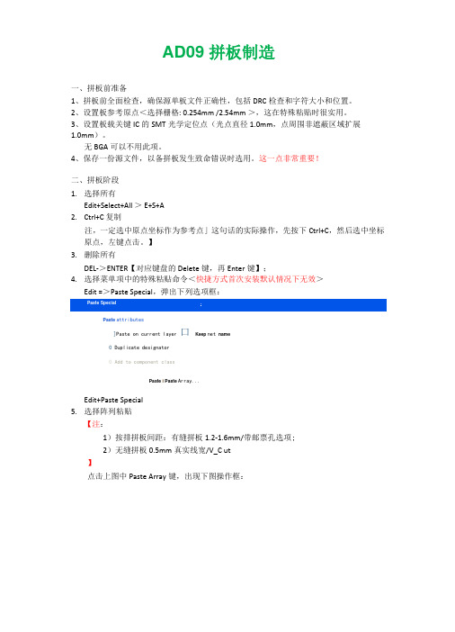
AD09 拼板制造一、拼板前准备1、拼板前全面检查,确保源单板文件正确性,包括DRC检查和字符大小和位置。
2、设置板参考原点<选择栅格: 0.254mm /2.54mm >,这在特殊粘贴时很实用。
3、设置板载关键IC的SMT光学定位点(光点直径1.0mm,点周围非遮蔽区域扩展1.0mm)。
无BGA可以不用此项。
4、保存一份源文件,以备拼板发生致命错误时选用。
这一点非常重要!二、拼板阶段1.选择所有Edit+Select+All > E+S+A2.Ctrl+C 复制注,一定选中原点坐标作为参考点」这句话的实际操作,先按下Ctrl+C,然后选中坐标原点,左键点击。
】3.删除所有DEL->ENTER【对应键盘的Delete键,再Enter键】;4.选择菜单项中的特殊粘贴命令<快捷方式首次安装默认情况下无效>Edit =>Paste Special,弹出下列选项框:Paste attributes]Paste on current layer 口Keep net name0 Duplicate designator0 Add to component classPaste i Paste Array...Edit+Paste Special5.选择阵列粘贴【注:1)按排拼板间距:有缝拼板1.2-1.6mm/带邮票孔选项;2)无缝拼板0.5mm真实线宽/V_C ut】点击上图中Paste Array键,出现下图操作框:上图中的各选项含义:1)Item Count 表示纵向或者横向的数目,由X-Spacing 或Y-Spacing 决定,即X-Spacing 或Y-Spacing 其中一个不为零的决定,二者必须一者为零;2)X-Spacing :板子的宽度+Vcut 的0.5或者有缝拼板1.2-1.6mm/带邮票孔; 3)Y-Spacing :板子的高度+Vcut 的0.5或者有缝拼板1.2-1.6mm/带邮票孔; 4) Linear :表示线性排列;选中参考点坐标(0,0)纵向陈列在粘贴后,如果提示有铜皮是否需要编译,选择NO.【此步的操作含义是粘贴,只要选中了参考点坐标(0,0),左键点击后自动粘贴。
NuMicro N9H30系列开发板用户手册说明书
NuMicro®FamilyArm® ARM926EJ-S BasedNuMaker-HMI-N9H30User ManualEvaluation Board for NuMicro® N9H30 SeriesNUMAKER-HMI-N9H30 USER MANUALThe information described in this document is the exclusive intellectual property ofNuvoton Technology Corporation and shall not be reproduced without permission from Nuvoton.Nuvoton is providing this document only for reference purposes of NuMicro microcontroller andmicroprocessor based system design. Nuvoton assumes no responsibility for errors or omissions.All data and specifications are subject to change without notice.For additional information or questions, please contact: Nuvoton Technology Corporation.Table of Contents1OVERVIEW (5)1.1Features (7)1.1.1NuMaker-N9H30 Main Board Features (7)1.1.2NuDesign-TFT-LCD7 Extension Board Features (7)1.2Supporting Resources (8)2NUMAKER-HMI-N9H30 HARDWARE CONFIGURATION (9)2.1NuMaker-N9H30 Board - Front View (9)2.2NuMaker-N9H30 Board - Rear View (14)2.3NuDesign-TFT-LCD7 - Front View (20)2.4NuDesign-TFT-LCD7 - Rear View (21)2.5NuMaker-N9H30 and NuDesign-TFT-LCD7 PCB Placement (22)3NUMAKER-N9H30 AND NUDESIGN-TFT-LCD7 SCHEMATICS (24)3.1NuMaker-N9H30 - GPIO List Circuit (24)3.2NuMaker-N9H30 - System Block Circuit (25)3.3NuMaker-N9H30 - Power Circuit (26)3.4NuMaker-N9H30 - N9H30F61IEC Circuit (27)3.5NuMaker-N9H30 - Setting, ICE, RS-232_0, Key Circuit (28)NUMAKER-HMI-N9H30 USER MANUAL3.6NuMaker-N9H30 - Memory Circuit (29)3.7NuMaker-N9H30 - I2S, I2C_0, RS-485_6 Circuit (30)3.8NuMaker-N9H30 - RS-232_2 Circuit (31)3.9NuMaker-N9H30 - LCD Circuit (32)3.10NuMaker-N9H30 - CMOS Sensor, I2C_1, CAN_0 Circuit (33)3.11NuMaker-N9H30 - RMII_0_PF Circuit (34)3.12NuMaker-N9H30 - RMII_1_PE Circuit (35)3.13NuMaker-N9H30 - USB Circuit (36)3.14NuDesign-TFT-LCD7 - TFT-LCD7 Circuit (37)4REVISION HISTORY (38)List of FiguresFigure 1-1 Front View of NuMaker-HMI-N9H30 Evaluation Board (5)Figure 1-2 Rear View of NuMaker-HMI-N9H30 Evaluation Board (6)Figure 2-1 Front View of NuMaker-N9H30 Board (9)Figure 2-2 Rear View of NuMaker-N9H30 Board (14)Figure 2-3 Front View of NuDesign-TFT-LCD7 Board (20)Figure 2-4 Rear View of NuDesign-TFT-LCD7 Board (21)Figure 2-5 Front View of NuMaker-N9H30 PCB Placement (22)Figure 2-6 Rear View of NuMaker-N9H30 PCB Placement (22)Figure 2-7 Front View of NuDesign-TFT-LCD7 PCB Placement (23)Figure 2-8 Rear View of NuDesign-TFT-LCD7 PCB Placement (23)Figure 3-1 GPIO List Circuit (24)Figure 3-2 System Block Circuit (25)Figure 3-3 Power Circuit (26)Figure 3-4 N9H30F61IEC Circuit (27)Figure 3-5 Setting, ICE, RS-232_0, Key Circuit (28)Figure 3-6 Memory Circuit (29)Figure 3-7 I2S, I2C_0, RS-486_6 Circuit (30)Figure 3-8 RS-232_2 Circuit (31)Figure 3-9 LCD Circuit (32)NUMAKER-HMI-N9H30 USER MANUAL Figure 3-10 CMOS Sensor, I2C_1, CAN_0 Circuit (33)Figure 3-11 RMII_0_PF Circuit (34)Figure 3-12 RMII_1_PE Circuit (35)Figure 3-13 USB Circuit (36)Figure 3-14 TFT-LCD7 Circuit (37)List of TablesTable 2-1 LCD Panel Combination Connector (CON8) Pin Function (11)Table 2-2 Three Sets of Indication LED Functions (12)Table 2-3 Six Sets of User SW, Key Matrix Functions (12)Table 2-4 CMOS Sensor Connector (CON10) Function (13)Table 2-5 JTAG ICE Interface (J2) Function (14)Table 2-6 Expand Port (CON7) Function (16)Table 2-7 UART0 (J3) Function (16)Table 2-8 UART2 (J6) Function (16)Table 2-9 RS-485_6 (SW6~8) Function (17)Table 2-10 Power on Setting (SW4) Function (17)Table 2-11 Power on Setting (S2) Function (17)Table 2-12 Power on Setting (S3) Function (17)Table 2-13 Power on Setting (S4) Function (17)Table 2-14 Power on Setting (S5) Function (17)Table 2-15 Power on Setting (S7/S6) Function (18)Table 2-16 Power on Setting (S9/S8) Function (18)Table 2-17 CMOS Sensor Connector (CON9) Function (19)Table 2-18 CAN_0 (SW9~10) Function (19)NUMAKER-HMI-N9H30 USER MANUAL1 OVERVIEWThe NuMaker-HMI-N9H30 is an evaluation board for GUI application development. The NuMaker-HMI-N9H30 consists of two parts: a NuMaker-N9H30 main board and a NuDesign-TFT-LCD7 extensionboard. The NuMaker-HMI-N9H30 is designed for project evaluation, prototype development andvalidation with HMI (Human Machine Interface) function.The NuMaker-HMI-N9H30 integrates touchscreen display, voice input/output, rich serial port serviceand I/O interface, providing multiple external storage methods.The NuDesign-TFT-LCD7 can be plugged into the main board via the DIN_32x2 extension connector.The NuDesign-TFT-LCD7 includes one 7” LCD which the resolution is 800x480 with RGB-24bits andembedded the 4-wires resistive type touch panel.Figure 1-1 Front View of NuMaker-HMI-N9H30 Evaluation BoardNUMAKER-HMI-N9H30 USER MANUAL Figure 1-2 Rear View of NuMaker-HMI-N9H30 Evaluation Board1.1 Features1.1.1 NuMaker-N9H30 Main Board Features●N9H30F61IEC chip: LQFP216 pin MCP package with DDR (64 MB)●SPI Flash using W25Q256JVEQ (32 MB) booting with quad mode or storage memory●NAND Flash using W29N01HVSINA (128 MB) booting or storage memory●One Micro-SD/TF card slot served either as a SD memory card for data storage or SDIO(Wi-Fi) device●Two sets of COM ports:–One DB9 RS-232 port with UART_0 used 75C3232E transceiver chip can be servedfor function debug and system development.–One DB9 RS-232 port with UART_2 used 75C3232E transceiver chip for userapplication●22 GPIO expansion ports, including seven sets of UART functions●JTAG interface provided for software development●Microphone input and Earphone/Speaker output with 24-bit stereo audio codec(NAU88C22) for I2S interfaces●Six sets of user-configurable push button keys●Three sets of LEDs for status indication●Provides SN65HVD230 transceiver chip for CAN bus communication●Provides MAX3485 transceiver chip for RS-485 device connection●One buzzer device for program applicationNUMAKER-HMI-N9H30 USER MANUAL●Two sets of RJ45 ports with Ethernet 10/100 Mbps MAC used IP101GR PHY chip●USB_0 that can be used as Device/HOST and USB_1 that can be used as HOSTsupports pen drives, keyboards, mouse and printers●Provides over-voltage and over current protection used APL3211A chip●Retain RTC battery socket for CR2032 type and ADC0 detect battery voltage●System power could be supplied by DC-5V adaptor or USB VBUS1.1.2 NuDesign-TFT-LCD7 Extension Board Features●7” resolution 800x480 4-wire resistive touch panel for 24-bits RGB888 interface●DIN_32x2 extension connector1.2 Supporting ResourcesFor sample codes and introduction about NuMaker-N9H30, please refer to N9H30 BSP:https:///products/gui-solution/gui-platform/numaker-hmi-n9h30/?group=Software&tab=2Visit NuForum for further discussion about the NuMaker-HMI-N9H30:/viewforum.php?f=31 NUMAKER-HMI-N9H30 USER MANUALNUMAKER-HMI-N9H30 USER MANUAL2 NUMAKER-HMI-N9H30 HARDWARE CONFIGURATION2.1 NuMaker-N9H30 Board - Front View Combination Connector (CON8)6 set User SWs (K1~6)3set Indication LEDs (LED1~3)Power Supply Switch (SW_POWER1)Audio Codec(U10)Microphone(M1)NAND Flash(U9)RS-232 Transceiver(U6, U12)RS-485 Transceiver(U11)CAN Transceiver (U13)Figure 2-1 Front View of NuMaker-N9H30 BoardFigure 2-1 shows the main components and connectors from the front side of NuMaker-N9H30 board. The following lists components and connectors from the front view:NuMaker-N9H30 board and NuDesign-TFT-LCD7 board combination connector (CON8). This panel connector supports 4-/5-wire resistive touch or capacitance touch panel for 24-bits RGB888 interface.Connector GPIO pin of N9H30 FunctionCON8.1 - Power 3.3VCON8.2 - Power 3.3VCON8.3 GPD7 LCD_CSCON8.4 GPH3 LCD_BLENCON8.5 GPG9 LCD_DENCON8.7 GPG7 LCD_HSYNCCON8.8 GPG6 LCD_CLKCON8.9 GPD15 LCD_D23(R7)CON8.10 GPD14 LCD_D22(R6)CON8.11 GPD13 LCD_D21(R5)CON8.12 GPD12 LCD_D20(R4)CON8.13 GPD11 LCD_D19(R3)CON8.14 GPD10 LCD_D18(R2)CON8.15 GPD9 LCD_D17(R1)CON8.16 GPD8 LCD_D16(R0)CON8.17 GPA15 LCD_D15(G7)CON8.18 GPA14 LCD_D14(G6)CON8.19 GPA13 LCD_D13(G5)CON8.20 GPA12 LCD_D12(G4)CON8.21 GPA11 LCD_D11(G3)CON8.22 GPA10 LCD_D10(G2)CON8.23 GPA9 LCD_D9(G1) NUMAKER-HMI-N9H30 USER MANUALCON8.24 GPA8 LCD_D8(G0)CON8.25 GPA7 LCD_D7(B7)CON8.26 GPA6 LCD_D6(B6)CON8.27 GPA5 LCD_D5(B5)CON8.28 GPA4 LCD_D4(B4)CON8.29 GPA3 LCD_D3(B3)CON8.30 GPA2 LCD_D2(B2)CON8.31 GPA1 LCD_D1(B1)CON8.32 GPA0 LCD_D0(B0)CON8.33 - -CON8.34 - -CON8.35 - -CON8.36 - -CON8.37 GPB2 LCD_PWMCON8.39 - VSSCON8.40 - VSSCON8.41 ADC7 XPCON8.42 ADC3 VsenCON8.43 ADC6 XMCON8.44 ADC4 YMCON8.45 - -CON8.46 ADC5 YPCON8.47 - VSSCON8.48 - VSSCON8.49 GPG0 I2C0_CCON8.50 GPG1 I2C0_DCON8.51 GPG5 TOUCH_INTCON8.52 - -CON8.53 - -CON8.54 - -CON8.55 - -NUMAKER-HMI-N9H30 USER MANUAL CON8.56 - -CON8.57 - -CON8.58 - -CON8.59 - VSSCON8.60 - VSSCON8.61 - -CON8.62 - -CON8.63 - Power 5VCON8.64 - Power 5VTable 2-1 LCD Panel Combination Connector (CON8) Pin Function●Power supply switch (SW_POWER1): System will be powered on if the SW_POWER1button is pressed●Three sets of indication LEDs:LED Color DescriptionsLED1 Red The system power will beterminated and LED1 lightingwhen the input voltage exceeds5.7V or the current exceeds 2A.LED2 Green Power normal state.LED3 Green Controlled by GPH2 pin Table 2-2 Three Sets of Indication LED Functions●Six sets of user SW, Key Matrix for user definitionKey GPIO pin of N9H30 FunctionK1 GPF10 Row0 GPB4 Col0K2 GPF10 Row0 GPB5 Col1K3 GPE15 Row1 GPB4 Col0K4 GPE15 Row1 GPB5 Col1K5 GPE14 Row2 GPB4 Col0K6GPE14 Row2GPB5 Col1 Table 2-3 Six Sets of User SW, Key Matrix Functions●NAND Flash (128 MB) with Winbond W29N01HVS1NA (U9)●Microphone (M1): Through Nuvoton NAU88C22 chip sound input●Audio CODEC chip (U10): Nuvoton NAU88C22 chip connected to N9H30 using I2Sinterface–SW6/SW7/SW8: 1-2 short for RS-485_6 function and connected to 2P terminal (CON5and J5)–SW6/SW7/SW8: 2-3 short for I2S function and connected to NAU88C22 (U10).●CMOS Sensor connector (CON10, SW9~10)–SW9~10: 1-2 short for CAN_0 function and connected to 2P terminal (CON11)–SW9~10: 2-3 short for CMOS sensor function and connected to CMOS sensorconnector (CON10)Connector GPIO pin of N9H30 FunctionCON10.1 - VSSCON10.2 - VSSNUMAKER-HMI-N9H30 USER MANUALCON10.3 - Power 3.3VCON10.4 - Power 3.3VCON10.5 - -CON10.6 - -CON10.7 GPI4 S_PCLKCON10.8 GPI3 S_CLKCON10.9 GPI8 S_D0CON10.10 GPI9 S_D1CON10.11 GPI10 S_D2CON10.12 GPI11 S_D3CON10.13 GPI12 S_D4CON10.14 GPI13 S_D5CON10.15 GPI14 S_D6CON10.16 GPI15 S_D7CON10.17 GPI6 S_VSYNCCON10.18 GPI5 S_HSYNCCON10.19 GPI0 S_PWDNNUMAKER-HMI-N9H30 USER MANUAL CON10.20 GPI7 S_nRSTCON10.21 GPG2 I2C1_CCON10.22 GPG3 I2C1_DCON10.23 - VSSCON10.24 - VSSTable 2-4 CMOS Sensor Connector (CON10) FunctionNUMAKER-HMI-N9H30 USER MANUAL2.2NuMaker-N9H30 Board - Rear View5V In (CON1)RS-232 DB9 (CON2,CON6)Expand Port (CON7)Speaker Output (J4)Earphone Output (CON4)Buzzer (BZ1)System ResetSW (SW5)SPI Flash (U7,U8)JTAG ICE (J2)Power ProtectionIC (U1)N9H30F61IEC (U5)Micro SD Slot (CON3)RJ45 (CON12, CON13)USB1 HOST (CON15)USB0 Device/Host (CON14)CAN_0 Terminal (CON11)CMOS Sensor Connector (CON9)Power On Setting(SW4, S2~S9)RS-485_6 Terminal (CON5)RTC Battery(BT1)RMII PHY (U14,U16)Figure 2-2 Rear View of NuMaker-N9H30 BoardFigure 2-2 shows the main components and connectors from the rear side of NuMaker-N9H30 board. The following lists components and connectors from the rear view:● +5V In (CON1): Power adaptor 5V input ●JTAG ICE interface (J2) ConnectorGPIO pin of N9H30Function J2.1 - Power 3.3V J2.2 GPJ4 nTRST J2.3 GPJ2 TDI J2.4 GPJ1 TMS J2.5 GPJ0 TCK J2.6 - VSS J2.7 GPJ3 TD0 J2.8-RESETTable 2-5 JTAG ICE Interface (J2) Function●SPI Flash (32 MB) with Winbond W25Q256JVEQ (U7); only one (U7 or U8) SPI Flashcan be used●System Reset (SW5): System will be reset if the SW5 button is pressed●Buzzer (BZ1): Control by GPB3 pin of N9H30●Speaker output (J4): Through the NAU88C22 chip sound output●Earphone output (CON4): Through the NAU88C22 chip sound output●Expand port for user use (CON7):Connector GPIO pin of N9H30 FunctionCON7.1 - Power 3.3VCON7.2 - Power 3.3VCON7.3 GPE12 UART3_TXDCON7.4 GPH4 UART1_TXDCON7.5 GPE13 UART3_RXDCON7.6 GPH5 UART1_RXDCON7.7 GPB0 UART5_TXDCON7.8 GPH6 UART1_RTSCON7.9 GPB1 UART5_RXDCON7.10 GPH7 UART1_CTSCON7.11 GPI1 UART7_TXDNUMAKER-HMI-N9H30 USER MANUAL CON7.12 GPH8 UART4_TXDCON7.13 GPI2 UART7_RXDCON7.14 GPH9 UART4_RXDCON7.15 - -CON7.16 GPH10 UART4_RTSCON7.17 - -CON7.18 GPH11 UART4_CTSCON7.19 - VSSCON7.20 - VSSCON7.21 GPB12 UART10_TXDCON7.22 GPH12 UART8_TXDCON7.23 GPB13 UART10_RXDCON7.24 GPH13 UART8_RXDCON7.25 GPB14 UART10_RTSCON7.26 GPH14 UART8_RTSCON7.27 GPB15 UART10_CTSCON7.28 GPH15 UART8_CTSCON7.29 - Power 5VCON7.30 - Power 5VTable 2-6 Expand Port (CON7) Function●UART0 selection (CON2, J3):–RS-232_0 function and connected to DB9 female (CON2) for debug message output.–GPE0/GPE1 connected to 2P terminal (J3).Connector GPIO pin of N9H30 Function J3.1 GPE1 UART0_RXDJ3.2 GPE0 UART0_TXDTable 2-7 UART0 (J3) Function●UART2 selection (CON6, J6):–RS-232_2 function and connected to DB9 female (CON6) for debug message output –GPF11~14 connected to 4P terminal (J6)Connector GPIO pin of N9H30 Function J6.1 GPF11 UART2_TXDJ6.2 GPF12 UART2_RXDJ6.3 GPF13 UART2_RTSJ6.4 GPF14 UART2_CTSTable 2-8 UART2 (J6) Function●RS-485_6 selection (CON5, J5, SW6~8):–SW6~8: 1-2 short for RS-485_6 function and connected to 2P terminal (CON5 and J5) –SW6~8: 2-3 short for I2S function and connected to NAU88C22 (U10)Connector GPIO pin of N9H30 FunctionSW6:1-2 shortGPG11 RS-485_6_DISW6:2-3 short I2S_DOSW7:1-2 shortGPG12 RS-485_6_ROSW7:2-3 short I2S_DISW8:1-2 shortGPG13 RS-485_6_ENBSW8:2-3 short I2S_BCLKNUMAKER-HMI-N9H30 USER MANUALTable 2-9 RS-485_6 (SW6~8) FunctionPower on setting (SW4, S2~9).SW State FunctionSW4.2/SW4.1 ON/ON Boot from USB SW4.2/SW4.1 ON/OFF Boot from eMMC SW4.2/SW4.1 OFF/ON Boot from NAND Flash SW4.2/SW4.1 OFF/OFF Boot from SPI Flash Table 2-10 Power on Setting (SW4) FunctionSW State FunctionS2 Short System clock from 12MHzcrystalS2 Open System clock from UPLL output Table 2-11 Power on Setting (S2) FunctionSW State FunctionS3 Short Watchdog Timer OFFS3 Open Watchdog Timer ON Table 2-12 Power on Setting (S3) FunctionSW State FunctionS4 Short GPJ[4:0] used as GPIO pinS4Open GPJ[4:0] used as JTAG ICEinterfaceTable 2-13 Power on Setting (S4) FunctionSW State FunctionS5 Short UART0 debug message ONS5 Open UART0 debug message OFFTable 2-14 Power on Setting (S5) FunctionSW State FunctionS7/S6 Short/Short NAND Flash page size 2KBS7/S6 Short/Open NAND Flash page size 4KBS7/S6 Open/Short NAND Flash page size 8KBNUMAKER-HMI-N9H30 USER MANUALS7/S6 Open/Open IgnoreTable 2-15 Power on Setting (S7/S6) FunctionSW State FunctionS9/S8 Short/Short NAND Flash ECC type BCH T12S9/S8 Short/Open NAND Flash ECC type BCH T15S9/S8 Open/Short NAND Flash ECC type BCH T24S9/S8 Open/Open IgnoreTable 2-16 Power on Setting (S9/S8) FunctionCMOS Sensor connector (CON9, SW9~10)–SW9~10: 1-2 short for CAN_0 function and connected to 2P terminal (CON11).–SW9~10: 2-3 short for CMOS sensor function and connected to CMOS sensorconnector (CON9).Connector GPIO pin of N9H30 FunctionCON9.1 - VSSCON9.2 - VSSCON9.3 - Power 3.3VCON9.4 - Power 3.3V NUMAKER-HMI-N9H30 USER MANUALCON9.5 - -CON9.6 - -CON9.7 GPI4 S_PCLKCON9.8 GPI3 S_CLKCON9.9 GPI8 S_D0CON9.10 GPI9 S_D1CON9.11 GPI10 S_D2CON9.12 GPI11 S_D3CON9.13 GPI12 S_D4CON9.14 GPI13 S_D5CON9.15 GPI14 S_D6CON9.16 GPI15 S_D7CON9.17 GPI6 S_VSYNCCON9.18 GPI5 S_HSYNCCON9.19 GPI0 S_PWDNCON9.20 GPI7 S_nRSTCON9.21 GPG2 I2C1_CCON9.22 GPG3 I2C1_DCON9.23 - VSSCON9.24 - VSSTable 2-17 CMOS Sensor Connector (CON9) Function●CAN_0 Selection (CON11, SW9~10):–SW9~10: 1-2 short for CAN_0 function and connected to 2P terminal (CON11) –SW9~10: 2-3 short for CMOS sensor function and connected to CMOS sensor connector (CON9, CON10)SW GPIO pin of N9H30 FunctionSW9:1-2 shortGPI3 CAN_0_RXDSW9:2-3 short S_CLKSW10:1-2 shortGPI4 CAN_0_TXDSW10:2-3 short S_PCLKTable 2-18 CAN_0 (SW9~10) Function●USB0 Device/HOST Micro-AB connector (CON14), where CON14 pin4 ID=1 is Device,ID=0 is HOST●USB1 for USB HOST with Type-A connector (CON15)●RJ45_0 connector with LED indicator (CON12), RMII PHY with IP101GR (U14)●RJ45_1 connector with LED indicator (CON13), RMII PHY with IP101GR (U16)●Micro-SD/TF card slot (CON3)●SOC CPU: Nuvoton N9H30F61IEC (U5)●Battery power for RTC 3.3V powered (BT1, J1), can detect voltage by ADC0●RTC power has 3 sources:–Share with 3.3V I/O power–Battery socket for CR2032 (BT1)–External connector (J1)●Board version 2.1NUMAKER-HMI-N9H30 USER MANUAL2.3 NuDesign-TFT-LCD7 -Front ViewFigure 2-3 Front View of NuDesign-TFT-LCD7 BoardFigure 2-3 shows the main components and connectors from the Front side of NuDesign-TFT-LCD7board.7” resolution 800x480 4-W resistive touch panel for 24-bits RGB888 interface2.4 NuDesign-TFT-LCD7 -Rear ViewFigure 2-4 Rear View of NuDesign-TFT-LCD7 BoardFigure 2-4 shows the main components and connectors from the rear side of NuDesign-TFT-LCD7board.NuMaker-N9H30 and NuDesign-TFT-LCD7 combination connector (CON1).NUMAKER-HMI-N9H30 USER MANUAL 2.5 NuMaker-N9H30 and NuDesign-TFT-LCD7 PCB PlacementFigure 2-5 Front View of NuMaker-N9H30 PCB PlacementFigure 2-6 Rear View of NuMaker-N9H30 PCB PlacementNUMAKER-HMI-N9H30 USER MANUALFigure 2-7 Front View of NuDesign-TFT-LCD7 PCB PlacementFigure 2-8 Rear View of NuDesign-TFT-LCD7 PCB Placement3 NUMAKER-N9H30 AND NUDESIGN-TFT-LCD7 SCHEMATICS3.1 NuMaker-N9H30 - GPIO List CircuitFigure 3-1 shows the N9H30F61IEC GPIO list circuit.Figure 3-1 GPIO List Circuit NUMAKER-HMI-N9H30 USER MANUAL3.2 NuMaker-N9H30 - System Block CircuitFigure 3-2 shows the System Block Circuit.NUMAKER-HMI-N9H30 USER MANUALFigure 3-2 System Block Circuit3.3 NuMaker-N9H30 - Power CircuitFigure 3-3 shows the Power Circuit.NUMAKER-HMI-N9H30 USER MANUALFigure 3-3 Power Circuit3.4 NuMaker-N9H30 - N9H30F61IEC CircuitFigure 3-4 shows the N9H30F61IEC Circuit.Figure 3-4 N9H30F61IEC CircuitNUMAKER-HMI-N9H30 USER MANUAL3.5 NuMaker-N9H30 - Setting, ICE, RS-232_0, Key CircuitFigure 3-5 shows the Setting, ICE, RS-232_0, Key Circuit.NUMAKER-HMI-N9H30 USER MANUALFigure 3-5 Setting, ICE, RS-232_0, Key Circuit3.6 NuMaker-N9H30 - Memory CircuitFigure 3-6 shows the Memory Circuit.NUMAKER-HMI-N9H30 USER MANUALFigure 3-6 Memory Circuit3.7 NuMaker-N9H30 - I2S, I2C_0, RS-485_6 CircuitFigure 3-7 shows the I2S, I2C_0, RS-486_6 Circuit.NUMAKER-HMI-N9H30 USER MANUALFigure 3-7 I2S, I2C_0, RS-486_6 Circuit3.8 NuMaker-N9H30 - RS-232_2 CircuitFigure 3-8 shows the RS-232_2 Circuit.NUMAKER-HMI-N9H30 USER MANUALFigure 3-8 RS-232_2 Circuit3.9 NuMaker-N9H30 - LCD CircuitFigure 3-9 shows the LCD Circuit.NUMAKER-HMI-N9H30 USER MANUALFigure 3-9 LCD Circuit3.10 NuMaker-N9H30 - CMOS Sensor, I2C_1, CAN_0 CircuitFigure 3-10 shows the CMOS Sensor,I2C_1, CAN_0 Circuit.NUMAKER-HMI-N9H30 USER MANUALFigure 3-10 CMOS Sensor, I2C_1, CAN_0 Circuit3.11 NuMaker-N9H30 - RMII_0_PF CircuitFigure 3-11 shows the RMII_0_RF Circuit.NUMAKER-HMI-N9H30 USER MANUALFigure 3-11 RMII_0_PF Circuit3.12 NuMaker-N9H30 - RMII_1_PE CircuitFigure 3-12 shows the RMII_1_PE Circuit.NUMAKER-HMI-N9H30 USER MANUALFigure 3-12 RMII_1_PE Circuit3.13 NuMaker-N9H30 - USB CircuitFigure 3-13 shows the USB Circuit.NUMAKER-HMI-N9H30 USER MANUALFigure 3-13 USB Circuit3.14 NuDesign-TFT-LCD7 - TFT-LCD7 CircuitFigure 3-14 shows the TFT-LCD7 Circuit.Figure 3-14 TFT-LCD7 CircuitNUMAKER-HMI-N9H30 USER MANUAL4 REVISION HISTORYDate Revision Description2022.03.24 1.00 Initial version NUMAKER-HMI-N9H30 USER MANUALNUMAKER-HMI-N9H30 USER MANUALImportant NoticeNuvoton Products are neither intended nor warranted for usage in systems or equipment, anymalfunction or failure of which may cause loss of human life, bodily injury or severe propertydamage. Such applications are deemed, “Insecure Usage”.Insecure usage includes, but is not limited to: equipment for surgical implementation, atomicenergy control instruments, airplane or spaceship instruments, the control or operation ofdynamic, brake or safety systems designed for vehicular use, traffic signal instruments, all typesof safety devices, and other applications intended to support or sustain life.All Insecure Usage shall be made at customer’s risk, and in the event that third parties lay claimsto Nuvoton as a result of customer’s Insecure Usage, custome r shall indemnify the damagesand liabilities thus incurred by Nuvoton.。
dfm 英文 制造流程

dfm 英文制造流程DFM in Manufacturing Processes.In the world of manufacturing, Design for Manufacturing (DFM) is a crucial concept that ensures the design of a product is optimized for efficient and cost-effective production. DFM considers the manufacturing constraints, capabilities, and processes early in the design stage, ensuring that the final design is not only aesthetically pleasing but also practical to produce.The primary goal of DFM is to identify and address potential manufacturing issues before the product goes into production. This approach helps to minimize redesigns, reduce waste, and improve overall product quality. DFM also aims to make the manufacturing process as efficient as possible, reducing lead times and costs.To achieve these goals, DFM involves a collaborative effort between designers, engineers, and manufacturingexperts. This teamwork ensures that the design considersall relevant factors, such as material selection, part complexity, assembly requirements, and production methods.Material Selection:DFM considers the impact of material choice on manufacturing processes. Different materials have unique properties that can affect the cost, time, and ease of manufacturing. For example, some materials may require special machining or finishing techniques, while others may be more suitable for certain production methods. By selecting materials that are compatible with the manufacturing processes, DFM can help to reduce costs and improve efficiency.Part Complexity:The complexity of a product's design can have a significant impact on manufacturing costs and lead times. DFM aims to simplify the design by identifying and eliminating unnecessary features or complexities that couldmake manufacturing more difficult or expensive. This might involve reducing the number of parts, simplifying geometry, or using standardized components.Assembly Requirements:DFM also considers the assembly process, ensuring that the design facilitates efficient and reliable assembly. This includes considering the order of assembly, the tools and equipment required, and the ease with which parts can be aligned and secured. By optimizing the assembly process, DFM can help to reduce production time, minimize defects, and improve overall product reliability.Production Methods:DFM is closely aligned with the manufacturing processes used to produce the product. It considers the capabilities and limitations of different production methods, such as machining, injection molding, casting, or additive manufacturing. By understanding these processes, DFM can help to design products that are compatible with the chosenproduction method, minimizing the need for expensive or time-consuming modifications later in the production cycle.In addition to considering these factors, DFM also involves the use of specialized tools and software to analyze and optimize the design. These tools can help to identify potential manufacturing issues early in the design process, allowing designers to make necessary changes before the product goes into production.The benefits of DFM are numerous. It can help to reduce manufacturing costs by minimizing waste, improving material utilization, and optimizing production processes. It can also shorten lead times by eliminating the need for redesigns or modifications later in the production cycle. Most importantly, DFM can improve product quality by ensuring that the design is robust and suitable for manufacturing.In conclusion, Design for Manufacturing (DFM) is a critical aspect of the manufacturing process. By optimizing the design for manufacturing constraints, capabilities, andprocesses, DFM can help to improve efficiency, reduce costs, and enhance product quality. It is an essential componentof any manufacturing strategy, enabling companies to compete effectively in today's global market.。
Athlete FA Corporation 半导体装配设备和装置设计文档说明书

BGA-CSP Systems are cutting-edge surface mount equip-SolidWorks EuropePhone: +33-(0)4-42-15-03-85Email:*************************Corporate HeadquartersDassault Systèmes SolidWorks Corporation 300 Baker AvenueConcord, MA 01742 USA Phone: +1-978-371-5011Email:*******************Japan Headquarters SolidWorks JapanTekko Building No. 1, 3F1-8-2 Marunouchi Chiyoda-Ku,Tokyo 100-0005 Japan Phone : +81-3-6270-8700Email:******************.jphttp://www.athlete-fa.co.jp/Gaining a competitive edge through tolerance optimization and verification using TolAnalyst The managing director of Planer Ltd., Mr. Hiroshi Kuriyama, worked for 25 years in design and development at Seiko Epson Inc. before establishing Planer in 2001. Mr . Kuriyama is currently a visiting professor at Nagano Technical College and a part-time lecturer in engineering at Shin-shu University. A keen supporter of Athlete FA’s enterprises, Mr . Kuriyama explains the relevance of tolerance analysis in the design process:“For the majority of manufactured goods, it is only after the design specifications and costing of the finished article have been decided - that is, only after the end goal is determined - that the creation of detailed designs begins. As products become increasingly miniaturised and multi-functional, so the demands placed on each of their individual components continually increase. If tolerance settings are tight, there is a corresponding jump in costs and it becomes difficult to meet delivery deadlines. So, in order to reach the end goal, that is the finished product, it is essential to achieve a balance through optimal tolerance design. Of course, without tolerance design it is impossible to maintain the quality of the end product.”In the past, tolerance design was considered to be tacit knowledge in the manufacturing indus-try, and as such was communicated from designer to designer on the job. However, due to a generational change in engineers and developments in the design environment, recently this method of knowledge transfer has become increasingly difficult. There are now overwhelming numbers of young designers across all sectors of the industry who do not know tolerance design theory. So, in collaboration with Planer, Athlete FA provided not only introductory and intermedi-ate SolidWorks seminars for their design engineers but also training for all employees in the basic principles of tolerance design.Having implemented the SolidWorks tolerance analysis tool, TolAnalyst, innovative activities such as comparing and verifying the results of manually calculated analysis are being tested. Through such activities the company aims to utilize the SolidWorks design tools to maximum effect.The Challenge: Athlete FA provided a 2-day lecture course in the fundamentals of tolerance design to all employees, including design engineers. Successful tolerance design has significant impact on cost, quality and time to market. Therefore, in addition to becoming profi-cient in using SolidWorks, design engi-neers need to be able to design product functionality itself that incorporates assembly and tolerance. A pioneering example in the equipment manufacturing industry, Athlete FA is proactively verify-ing the analytical results of tolerance optimization obtained by manual calcula-tion and those obtained using the Solid-Works TolAnalyst.The Solution: In the design section at Athlete FA there is one SolidWorks seat per engineer. Thanks to a comprehensive training program for all employees and the creation of a standard operation manual covering features, modelling and assembly, the skill level of all engineers is consistent. To make full use of the benefits of a transition to 3D, a set of standard design guidelines was estab-lished on the basis of detailed consulta-tions at the time of introducing Solid-Works. All Athlete FA products are now designed using SolidWorks.A 3D model of the Micro Ball Mounter BM-1100W created in SolidWorksA drawing of th e main unit of th e CSP-capable BGA Ball Mounting System BA-1500PP sketched by Athlete FA design engineers (to give a simple example). There are 39 tolerance factors in total, 19 dimensional and 20 geometrical tolerance factors. Using tolerance design th e possibilities for optimizing tolerance distribution (cost reduction) and eliminating th e need to readjust tolerance have widened.Analytical results produced by TolAnalyst (first section only shown here). Calculating tolerance in mainly height directions would take approximately half a day to calculate manually but is completed in around 20-30 minutes with TolAnalyst.Athlete FA CorporationHeadquarters: 2970-1 Shiga, Suwa City, Nagano, JapanEstablished: March 1, 1988Business outline: Factory Automation Engineering- Development, design and marketing of a range of high-precision mount-ing and assembly systems for vari-ous industrial applications including office automation equipment, semi-conductors, electronic components, automobiles, and communications devices.- Design, manufacture and marketing of automation equipment.。
Allegro-PCB后处理
Allegro PCB后处理——孙海峰在完成PCB的布局、布线和覆铜工作后,要做些后续处理工作,包括可装配性检查、测试点生成等,而后才能输出可供厂家生产的PCB光绘文件。
接下来按照顺序,来具体阐述Allegro PCB 的后处理。
一、设计的可装配性检查设计的可装配性检查就是DFA检查,是检查设计中的元件装配方面问题。
检查对象包括:元件间距、引脚跨距、焊盘跨距轴向、过孔及测试点等。
在可装配性检查时,PCB设计中与约束不一致时将会以DRC形式标示出来。
在Allegro PCB工作界面中执行Manufacture/DFx check(legacy)命令,弹出Design For Assembly对话框,可进行设计的可装配性检查。
在该对话框中,点击Constraint Setup可对设计的可装配性进行规则设置,如下图,点击Run Audit可根据规则设置进行DFA检查,点击Report即可查看检查报告。
接下来,对DFA Audit Setup对话框进行详细的解释,这也就是可装配性检查的基本项目介绍。
1、检查元件间距为了确保满足组装、调试和维修所需要的元件间隔要求,在PCB完成后,还需要对元件间距进行检查。
在DFA Audit Setup对话框中,点击component_clearance_audit/Default,则在下方Constraints窗口进行规则设置。
其中可设置:设定规则名称;选择所需检查元件间距的两元件;规则具体设置。
其中:Edge1和Edge2设定间隔检查时所用元件的边界,Layer设定检查间距的板层,Units设定显示单位,Spacing设定最小间距,Subclass设定检查元件间距时按照Assembly还是Place_Bound层。
2、检查元件元件检查包括:(1)元件摆放方向是否适合焊接;(2)元件是否摆放在允许摆放的两个板层Top、Bottom或者Either。
在DFA Audit Setup对话框中点击component_orientation_layer_audit,在下方Constraints窗口如下图。
流程图相关英语作文

流程图相关英语作文Title: The Importance and Application of Flowcharts。
Flowcharts are essential tools in various fields, providing a visual representation of processes, systems, or workflows. They play a crucial role in organizing, understanding, and communicating complex information. This essay explores the significance of flowcharts and their applications across different domains.Firstly, flowcharts serve as a universal language for conveying processes and procedures. Regardless of language barriers, individuals can interpret a flowchart's symbols and understand the sequence of steps involved in a process. This universality makes flowcharts an effective communication tool in multicultural and multinational environments.Moreover, flowcharts enhance clarity and comprehension. By breaking down complex processes into manageable stepsand illustrating decision points, flowcharts simplify intricate concepts. Whether used for training purposes or troubleshooting procedures, flowcharts enable individuals to grasp information quickly and accurately.In addition to their communicative benefits, flowcharts aid in process optimization and efficiency improvement. By visualizing workflows, stakeholders can identify bottlenecks, redundancies, or inefficiencies within a system. This insight empowers organizations to streamline processes, allocate resources effectively, and enhance overall productivity.Furthermore, flowcharts facilitate problem-solving and decision-making processes. When faced with a challenge or dilemma, individuals can refer to a flowchart to determine the appropriate course of action. The structured layout of a flowchart guides users through logical steps, helping them arrive at solutions efficiently.The versatility of flowcharts extends across various industries and sectors. In the field of softwaredevelopment, flowcharts are instrumental in designing algorithms, defining software architecture, and mapping out user interfaces. Similarly, in manufacturing and production environments, flowcharts aid in optimizing assembly lines, inventory management, and quality control processes.In project management, flowcharts assist in planning, scheduling, and tracking project milestones. They visualize the sequential flow of tasks, dependencies between activities, and critical paths. Project managers rely on flowcharts to ensure projects stay on track and meet deadlines effectively.Furthermore, flowcharts find applications in healthcare, where they depict patient care pathways, treatment protocols, and medical decision-making processes. By visualizing healthcare workflows, clinicians can enhance patient safety, optimize resource utilization, and improve overall quality of care.In the realm of education, flowcharts are valuable instructional tools for explaining complex concepts,illustrating problem-solving strategies, and guiding students through procedural tasks. Teachers utilize flowcharts to engage students visually and enhance their understanding of academic subjects.Overall, flowcharts play a vital role in organizing information, facilitating communication, optimizing processes, and guiding decision-making across diverse domains. Their universal appeal, clarity-enhancing features, and versatility make them indispensable tools in today's complex and dynamic world.In conclusion, flowcharts represent more than just graphical representations of processes; they are powerful instruments for fostering understanding, efficiency, and innovation. Whether in business, technology, healthcare, education, or any other field, flowcharts continue to shape the way we visualize, analyze, and improve processes. Embracing the utility of flowcharts enables individuals and organizations to navigate complexity with clarity and confidence.。
zbc埋入式电容的英文单词
zbc埋入式电容的英文单词The English word for "zbc埋入式电容" is "embedded capacitor".Embedded capacitors, also known as buried capacitors, are an essential component in modern electronic devices and circuits. They are designed to provide capacitance within the circuit board itself, eliminating the need for discrete capacitors. This integration not only saves space but also improves the overall performance and reliability of the electronic system.The concept of embedded capacitors involves incorporating a layer of dielectric material with a high dielectric constant into the printed circuit board (PCB) itself. This dielectric layer acts as a capacitor, capable of storing and releasing electrical energy. The dielectric material used in embedded capacitors is typically a high-performance polymer or ceramic with excellent electrical properties.One of the main advantages of embedded capacitors is their ability to minimize the parasitic inductance and resistance associated with discrete capacitors. In traditional PCB designs, the leads and traces connecting the capacitors introduce parasitic elements that can degrade the performance of the circuit. By integrating the capacitor directly into the PCB, these parasitic elements are significantly reduced, leading to improved signal integrity and faster response times.Embedded capacitors also offer enhanced thermal management capabilities. By distributing the capacitors throughout the PCB, heat generated during operation can be dissipated more efficiently. This reduces the risk of overheating and improves the overall reliability of the electronic device.Furthermore, the integration of capacitors into the PCB simplifies the assembly process and reduces manufacturing costs. The need for manual placement of discrete capacitors is eliminated, saving time and reducing the risk of human error. Additionally, the smaller form factor of embedded capacitors allows for higher-density circuit designs, further optimizing the use of available space on the PCB.The application of embedded capacitors is widespread across various industries, including telecommunications, automotive, aerospace, and consumer electronics. They are commonly used in power management circuits, high-frequency filters, decoupling networks, and signal conditioning circuits. The demand for embedded capacitors continues to grow as electronic devices become more compact and require higher performance levels.In conclusion, "zbc埋入式电容" translates to "embedded capacitor" in English. Embedded capacitors offer numerous benefits, including improved circuit performance, enhanced thermal management, reduced manufacturing costs, and increased design flexibility. As electronic devices continue to evolve, embedded capacitors play a crucial role in enabling smaller, more efficient, and reliable systems.。
最详细的FLEXA编程教程
设定供料器中是否存在料卷托架。如果将其设定为“Reel holder”,则根据料卷托架式供料器的搭载条件执行优化。如果将其设定为“Reel Holder-E”,则根据料斗型供料器托架的供料器搭载条件执行优化
Configuration 设定的各项解释
Optimize NozzleStation
Job编辑器的优化 Job编辑器的优化 如果是制作程式,建议重新配置供料器。如果是修改程式,建议不要勾选。
选择要优化的机器
Job编辑器的优化
2.Job编辑器的优化
注意: 不要优化一半,按终止 影响优化效果
优化 到无错误发生,并检查数据是否各个模组已经很平衡。如果单一模组不能平衡,找出原因。尽量做到各个模组平衡,提高机器利用率
Conveyor Mode
Dual
用于设定电路板的搬运方法,在执行优化时被参照
Target Conveyor
Lane1
设定进行Job 优化的通道。如果选择“Lane 1”,则优化通道1 上进行生产Job
Optimizer Type
Speed
选择“Speed”进行优化后,实际生产周期时间会 相对变短。选择“Optimal”进行优化后,实际生 产周期时间会变为最短,但此方法所需优化处理 时间最长。“Time Limit”则是在规定时间(分 钟)内进行和“Optimal”相同的优化处理。
Feeder Duplication
Yes
在贴装多贴装数的元件时,设定是否将元件分配给多个供料器并分配给其他模组。如果设定为“Yes”,则将贴装数较多的元件分配给多个供料器,并且在多个模组上进行贴装
Configuration 设定的各项解释
Use Current Feeder Setup
GenFlex菜单命令中英文对照
Custom 钻-铜定制优化 Lecagy做间距
Legend Detection 文字侦测 Construct Pads(Auto.) 自动换pad Construct Pads(Auto.All Angles) 自动换pad,无论角度
大小,建议不用 Construct Pads(Ref.) 手动换pad Set SMD Attribute 设定SMD属性 Line Unification 线路简化(合并线) Redundant Line Removal 重复多余的线路删除 NFP Removal 无功能独立点删除(删除独立PAD) Drawn to Outline 绘制外框线(以线或轮廓来代替线绘
Step Compare 料号对比 Multi Layer Copy 焊接层拷贝 Quote Summary 引用数据
New 新的Checklist Open 开启Checklist Rename 更改Checklist名称 Delete 删除Checklist Copy From Library 将其从数据库copy出来 Copy To Library 将其 copy至数据库
File 档案 Save 存档 Script 自动化程序
Locks 锁住的管理
Print Layer 打印 Close 结束
Alt + F + S 养成随时保存的好习惯。
Run 执行程式 Record 录制指令 History 查看指令历史 Binding 连结(对应快速键) Debug 程式除错器 Continue 暂停继续 Check Out 开启 Check In 关闭 Lock Status 状态
Critcal Via Analysis 关键导通孔检查
编译器keil的优化选项针对ARM
编译器_keil的优化选项问题分类:编译器类2013-01-11 14:12 280人阅读评论(0) 收藏举报applicationApplicationcompilationcompileroptimizationperformancePerformance最近发现在keil编译的时候,出现莫名的问题,貌似代码有被优化掉的问题,后来查了下相关的资料,貌似懂了点。
我选择的是默认的default优化方式,上网看了下,默认的是level2级别优化,最后选择level0就没有问题了下面是网上找的资料,介绍了优化功能介绍Getting the Best Optimized Code for your Embedded ApplicationARM Compilation ToolsThe ARM Compilation Tools are the only compilation tool s co -developed with the ARM processors, and specificallydesigned to optimally support the ARM architecture. They are a result of 20 years of development, and are recognized as theindustry -leading C and C++ compilation tools for the ARM, Thumb, and Thumb -2 instructions sets.The ARM Compilation tools consist of:• The ARM Compiler, which enables you to compile C and C++ code. It is an optimizing compiler, and featurescommand - line options to enable you to control the level of optimization• Linker and Utilities, which assign addresses and lay out sections of code to form a final image• A selection of libraries, including the ISO standard C libraries, and the MicroLIB C library which is optimized forembedded applications• Assembler, which generates machine code instructions from ARM, Thumb orThumb-2 assembly- level source codeCompiler Options for Embedded ApplicationsThe ARM Compilation Tools include a number of compiler optimizations to help you besttarget your code for your chosenmicrocontroller device and application area.They can be accessed from within µVision by clicking on Project –Options for Target. T he options described this document can be found on the Target and C/C++ tabs of the Options for Targets dialog.MDK Compiler Optimizations• Cross- ModuleOptimization takes information from a prior build and uses it to place UNUSED functions into theirown ELF section in the corresponding object file. This option is also known as Linker Feedback, and requires you tobuild your application twice to take adv antage of it for reduced code size.Cross-Module Optimization has been shown to reduce code size, by removing unused functions from your application. Itcan also improve the performance of your application, by allowing modules to share inline code.• The M icroLIB C libraryhas been optimized to reduce the size of embedded applications. It is a subset of the ISOstandard C runtime library, and offers a tradeoff between functionality and code size. Some of the standard C libraryfunctions such as memcpy() are slower, while some features of the default library are not supported. Unsupportedfeatures include:o Operating system functions e.g. abort(), exit(), time(), system(), getenv(),o Wide character and multi-byte support e.g. mbtowc(), wctomb()o The stdio file I/O function, with the exception of stdin, stdout and stderro Position-independent and thread -safe codeUse the MicroLIB C library for applications where overall performance can be traded off against the need to reduce codesize and memory cost.• Link- Time Code Generation instructs the compiler to create objects in an intermediate format so that the linker canperform further code optimizations. This gives the code generator visibility into cross - file dependencies of all objectssimultaneously, allowing it t o apply a higher level of optimizations. Link -time code generation can reduce code size, andallow your application to run faster.• Optimization Levels can also be adjusted. The different levels of optimization allow you to trade off between the levelof debug information available in the compiled code, and the performance of the code. The following optimization levelsare available:o - O0 applies minimum optimizations.Most optimizations are switched off, and the code generated has the best debug view.o - O1 applies restricted optimization.For example, unused inline functions and unused static functions are removed. At this level of optimization, thecompiler also applies automatic optimizations such as removing redundant code and re -ordering instructions s oas to avoid an interlock situation. The code generated is reasonably optimized, with a good debug view.o - O2 applies high optimization (This is the default setting).Optimizations app lied at this level take advantage of ARM’s in-depth knowledge of the processor architecture,to exploit processor -specific behavio r of the given target. It generates well optimized code, but with limiteddebug view.o - O3 applies th e most aggressive optimization.The optimization is in accordance with the user’s – Ospace/- Otime choice . By default, multi - file compilation isenabled, which leads to a longer compile time, but gives the highest levels ofoptimization.• The Optimize for Time checkbox causes the compiler to optimize with a greater focus on achieving the bestperformance when checked ( - O time) or the smallest code siz e when unchecked ( -O space).Unchecking Optimize for Time selects the – Ospace option which instructs the compiler to perform optimizations toreduce the image size at the expense of a poss ible increase i n execution time. F or example, using out -of -line functioncalls instead of inline code for large structure copies. This is the default option. When running the compiler from thecommand line, this option is invoked using ‘ -Ospace’Checking Optimize for Time selects the – Otime option which instructs the compiler to optimize the code for the fastestexecution time, at the risk of an increase in the image size. It is recommended that you compile the time -critical parts ofyour code with – Otime, and the rest us ing the – Ospace directive .• Split Load and Store Multiples instructs the compiler to split LDM and STM instructions involving a large number ofregisters into a series of loads/stores of fewer multiple registers. This means that an LDM of 16 registers can be split into4 separate LDMs of 4 registers each. This option helps to reduce the interrupt latency on ARM systems which do nothave a cache or write buffer, and systems which use zero - wait state 32-bit memory.For example, the ARM7 and ARM9 processor s t ake can only take an exception on an instruction boundary. If anexception occurs at the start of an LDM of 16 registers in a cacheless ARM7/ARM9 system, the system will finishmaking 16 accesses to memory before taking the exception. Depending on the memory arbitration system, this can resultin a very high interrupt latency. Breaking the LDM into 4 individual LDMs for 4 registers means that the processor willtake the exception after loading a maximum of 4 registers, thereby greatly reducing theinterrupt latency.Selecting this option improves the overall performance of the system.• The One ELF Section per Function option tells the compiler to put all functions into their own individual ELFsections. This allows the linker to remove unused functions.An ELF code section typically contains the code for a number of functions. The linker is normally only able to removeunused ELF sections, not unused functions. An ELF section can only be removed if all its contents are unused.Therefore, splitting each function into its own ELF section allows the compiler to easily identify which ones are unused,and remove them.Selecting this option increases the time required to compile your code, but results in improved performance .The combination of options applied will depend on your optimization goal – whether you are optimizing for smallest codesize, or best performance.The next section illustrates the best optimization options for each of these goals.Optimizing for Smallest Code SizeTo optimize your code for the smallest size, the best options to apply are:• The MicroLIB C library• Cross- module optimization• Optimization level 2 ( -O2)Compile the Measure example without any optimizationsThe Measure example uses analog and digital inputs to simulate a data l ogger.File -- Open ProjectC: \Keil \ARM\Boards \Keil \MCBSTM32\Measure\Measure.uv2Click the Options for Target buttonIn the Target tab:• Uncheck Cross- Module Optimization• Uncheck Use MicroLIB• Uncheck Use Link- Time Code GenerationIn the C/C++ tab:• Set Optimization Level to ZeroThen click OK to save your changes.Project – Build targetWithout any compiler optimizations applied, the initial code size is 13,656 Bytes.MDK Compiler OptimizationsOptimize the Measur e example for SizeApply the compiler optimizations in turn, and re-compile each time to see their effect in reducing the code size for theexample.• Options for Target – Target tab: Use the MicroLIB C library• Options for Target – Target tab: Use cross - mod ule optimization - Remember to compile twice• Options for Target –C/C++ tab: Enable Optimization level 2 ( -O2)Optimization Applied Compile Size Size Reduction ImprovementMicroLIB C library 8,960 Bytes 4,696 Bytes 34% smallerCross- Module Compilation 13,500 Bytes 156 Bytes 1.1% smallerOptimization level – O2 12,936 Bytes 720 Bytes 5.3% smallerAll 3 optimization options 8,116 Bytes 5,540 Bytes 40.6% smallerApplying all the optimizations will reduce the code size down to 8,116 Bytes.The fully optimized code is 5,540 Bytes smaller, a total code size reduction of 40.6%MDK Compiler OptimizationsOptimizing for Best PerformanceTo optimize your code for performance, the best options to apply are:• Cross- module optimization• Optimization level 3 ( -O3)• Optimize for timeRun the Dhrystone benchmark without any optimizationsThe Dhrystone benchmark is used to measure and compare the performance of different computers, or the efficiency of thecode generated for the same computer by different compilers.File –Open ProjectC: \Keil \ARM\Examples \DHRY \DHRY.uv2Click the Options for Target buttonTurn off optimization settings in the Target and C/C++ tabs , thenclick OKProject – Build targetEnter D ebug modeView –Se rial Windows –UART #1Open the UART #1 windowView –Analysis Windows –Performance AnalyzerOpen the Performance AnalyzerDebug –RunStart running the applicationWhen prompted:Enter 50000 in the UART#1 window and press EnterIn the Performance Analyzer window, note that• The drhy_1 loop took 2.829s• The dhry_2 took 2.014sIn the UAR T #1 window, note that• It took 138.0 ms for 1 run through Dhrystone• The application is executing 7246.4 Dhrystones per secondOptimize the Dhrystone example for PerformanceRe-compile the example with all three of the following optimizations applied:• Options f or Target – Target tab: Cross - module optimization –Remember to compile twice• Options for Target –C/C++ tab: Optimization level 3 ( -O3)• Options for Target –C/C++ tab: Optimize for TimeRe-run the application, and examine the performance.Measurement Without optimizations With Optimizations Improvementdhry_1 2.829s 1.695s 40.1% fasterdhry_2 2.014s 1.011s 49.8% fasterMicroseconds for 1 runthrough Dhrystone138.0 70 49.3% fasterDhrystones per second 7246.4 14,285.7 97.1% moreThe fu lly optimize d code achieves approximate ly 2x the performance of the un-optimized code.SummaryThe ARM Compilation Tools offer a range of options to apply when compiling your code. These options can be combined tooptimize your code for best performance, for smallest code size, or for any performance point between these two extremes, tobest suit your targeted microcontroller device and market.When optimizing your code, MDK- ARM makes it easy and convenient to measure the effect of the different optimizationsett ings on your application. The code size is clearly displayed after compilation, and a range of analysis tools such as thePerformance Analyzer enable you to measure performance.The optimization options in the ARM Compilation Tools, together with the easy- to - use analysis tools in MDK - ARM, helpyou to easily optimize your application to meet your specific requirements.获得最佳优化的代码为您的嵌入式应用ARM编译工具ARM编译工具是唯一的编译工具与ARM处理器共同开发,并专门最佳支持ARM架构。
- 1、下载文档前请自行甄别文档内容的完整性,平台不提供额外的编辑、内容补充、找答案等附加服务。
- 2、"仅部分预览"的文档,不可在线预览部分如存在完整性等问题,可反馈申请退款(可完整预览的文档不适用该条件!)。
- 3、如文档侵犯您的权益,请联系客服反馈,我们会尽快为您处理(人工客服工作时间:9:00-18:30)。
Research articleOptimizing PCB assembly for familysetup strategyY ongzhong Wu and P.JiIndustrial and Systems Engineering,The Hong Kong Polytechnic University,Kowloon,People’s Republic of China,andWilliam HoAston University,Aston,UKAbstractPurpose–The purpose of this paper is to investigate the optimization for a placement machine in printed circuit board(PCB)assembly when family setup strategy is adopted.Design/methodology/approach–A complete mathematical model is developed for the integrated problem to optimize feeder arrangement and component placement sequences so as to minimize the makespan for a set of PCB batches.Owing to the complexity of the problem,a specific genetic algorithm(GA)is proposed.Findings–The established model is able tofind the minimal makespan for a set of PCB batches through determining the feeder arrangement and placement sequences.However,exact solutions to the problem are not practical due to the complexity.Experimental tests show that the proposed GA can solve the problem both effectively and efficiently.Research limitations/implications–When a placement machine is set up for production of a set of PCB batches,the feeder arrangement of the machine together with the component placement sequencing for each PCB type should be solved simultaneously so as to minimize the overall makespan.Practical implications–The paper investigates the optimization for PCB assembly with family setup strategy,which is adopted by many PCB manufacturers for reducing both setup costs and human errors.Originality/value–The paper investigates the feeder arrangement and placement sequencing problems when family setup strategy is adopted,which has not been studied in the literature.Keywords Assembly,Printed circuits,Process planning,Process efficiencyPaper type Research paper1.IntroductionPrinted circuit board(PCB)assembly consists of mounting electronic components onto a bare board by the so-called placement machines(Figure1).A typical placement machine has a feeder carrier,a PCB holder,and a placement device. The feeder carrier consists of many feeder slots where the component feeders are located.The component feeders are used to provide the machine with a continuous supply of components.Generally,the placement device picks components from the feeders and places them onto the board.According to different operation modes,the placement machines can be classified into different types,e.g.sequential pick-and-place machines,turret-type machines,collect-and-place machines,multi-station machines(Figure1shows the first two machine types).Optimization of the feeder setup and component placement sequence are two most important factors for improving the efficiency of placement machines.They correspond to two fundamental subproblems for machine optimization,i.e.the feeder arrangement problem(FAP)and the placement sequencing problem(PSP).The FAP is to decide the assignment of different component feeders to the slots on the feeder carrier,while the PSP is to decide the placement sequence of the components.Nowadays,many PCB manufacturers face with the difficulties caused by the wide variety of products.High-mix environment often requires frequent machine setups.While the batch sizes are small,setup time may constitute as great as 50percent of the total production time(Jain et al.,1996). Therefore,families of similar PCBs are clustered so that setups are only required between switching of families.This setup strategy is referred to as family setup strategy. However,the family setup strategy makes the already complicated machine optimization problems even more difficult.When a family setup is adopted,the machine is required to be set up for a family of boards.In this situation, the feeder arrangement and placement sequence should be optimized with respect to multiple boards.The current issue and full text archive of this journal is available at /0144-5154.htmAssembly Automation29/1(2009)61–67q Emerald Group Publishing Limited[ISSN0144-5154][DOI10.1108/01445150910929875]This research investigates the optimization of feeder arrangement and placement sequencing for a PCB placement machine adopting a family setup strategy,i.e.the placement machine is set up (feeder arrangement)once for a set of PCB batches.The paper is organized as follows.Literature relating to machine optimization problems in PCB assembly is surveyed in Section 2.In Section 3,a complete mathematical model for the problem is established.In Section 4,the model is verified through solving some problem instances.A specific genetic algorithm (GA)for the problem is proposed and described in Section 5.Finally,the paper is concluded in Section 6.2.Literature reviewThere are many planning problems in PCB assembly owing to the great variety of production environments concerning shop layout,production mix,setup policy,etc.These problems can be classified according to different planning levels on the planning hierarchy.This paper focuses on the optimization of a single placement machine.For the optimization of an assembly line with multiple machines,one may refer to Sze et al.(2001)and Wan and Ji (2001).Numerous researchers have investigated machine optimization problems in PCB assembly,i.e.feeder arrangement and PSP .Owing to the complexity of these two problems,some researchers focused on only one of them,while assuming the solution to the other is given in advance (Drezner and Nof,1984;Ball and Magazine,1988;Moyer and Gupta,1996a,b;Ahmadi and Mamer,1999;Klomp et al.,2000;Kim and Park,2004;Li et al.,2007).However,most researchers agree that these two problems are intertwined with each other to influence the efficiency of the machine,and should be considered at the same time.Some researchers focused on an approach that consists of tackling both problems by iterating between (heuristic)both solutions.Among these,Foulds and Hamacher (1993)used an iterative approach for a sequential pick-and-place machine.The PSP was solved by a TSP heuristic and the feeder arrangement problem was solved by a QAP heuristic.Egbelu et al.(1996)also considered a sequential pick-and-place machine and solved the two problems with two heuristics iteratively.Crama et al.(1990)solved the two problems iteratively for a collect-and-place machine,with each problem solved by a heuristic.Leipa ¨la ¨and Nevalainen (1989)stated that the iterative approach was fast but obtained inferior solutions.For this reason,many other researchers proposed approaches for solvingthe two problems simultaneously.Broad et al.(1996)established an integrated integer programming (IP)model for the two problems for a sequential pick-and-place machine.The model was solved by a binary IP package.Leu et al.(1993)proposed a two-link GA to simultaneously solve the feeder arrangement and PSP for both a sequential pick-and-place and a turret-type machine.Ho and Ji (2003,2004)modified the two-link GA proposed by Leu et al.for both a sequential pick-and-place and a turret-type machine and obtained better results.Moyer and Gupta (1996a,b)proposed a heuristic called AAT for solving the two problems simultaneously for a turret-type machine.They also stated that on average,their approach was superior to the GA proposed by Leu et al.(1993).Y eo et al.(1996)proposed a rule-based approach to simultaneously solve the feeder arrangement problem and PSP for a turret-type machine.Ellis et al.(2001)proposed a heuristic for solving the two problems simultaneously for a turret-type machine.They used a construction procedure with a set of rules to generate an initial component placement sequence and feeder arrangement,and an improvement procedure to improve the initial solution.Some researchers studied the optimization problems for some more advanced placement machines.Kulak et al.(2007)proposed GA for collect-and-place machines with revolving heads.Ho et al.(2007)also proposed a GA to solve the feeder arrangement and PSP simultaneously for a dual-gantry collect-and-place machine.Wang et al.(1999)proposed a GA to optimize feeder setup for a multi-station placement machine.Recently,Grunow et al.(2003)established an IP model for the optimization of a multi-station machine.It can be seen from the survey that numerous researchers have investigated the machine optimization problems in PCB assembly.However,all the researchers considered optimizing a machine for a single board type.T o the best of our knowledge,no researchers have considered the situation when a machine is set up for production of multiple boards,i.e.the family setup strategy is adopted.3.A mathematical modelSince the investigated problem has not been investigated by other researchers,a mathematical model for the problem is required.In this paper,the sequential pick-and-place machine (as shown in Figure 1(a))is studied.For a sequential pick-and-place machine,the placement head can move in the X -Y plane.After the placement head travels to a feeder and picks a component,it moves to the placing location on the board and places the component.Then it travels to another feeder to pickFigure 1Different PCB placement machine types(a) Sequential pick-and-place (b) Turret-typeFeedersup another component.The same operations are repeated until all required components are placed on the board.As discussed earlier,optimization of placement machines consists of solving the feeder arrangement problem,which deals the assignment of different component feeders to different feeder slots on the machine,and the PSP,which decides the sequence for the components to be placed.These two problems intertwine with each other to influence the process time for a specific board.When the machine is set up for producing different board types,the feeder arrangement problem should consider the characteristics of all the board types.At the same time,different placement sequences corresponding to different board types should also be determined.The optimization of feeder arrangement and placement sequencing should aim to minimize the makespan for all PCB batches.Here,an integrated mathematical model for the stated problem is established.The parameters and variables used in this model are defined as follows:1Parameters:.t ijs ,time elapsed between placing component i and placing component j when feeder f (j )is stored in slot s ;.n ,total number of components on all board types;.m ,number of board types;.n h ,number of components on a PCB of type h ;.q i ,batch size of the PCB that consists of component i ;.n ,total number of component types;.c ,total number of feeder slots on the machine;.C h ,set of components on a PCB of type h ;and .G h ,arbitrary (n h 21)components on a PCB of type h .2Decision variables:.x ij ,0-1variables.x ij ¼1if component j is placed immediately after component i (i ,j ¼1,...,n );.y f (i ),s ,0-1decision variables.y f (i ),s ¼1if a feeder type for component i is stored in slot s ;and .u i ,auxiliary integer variables,indicating the placement order of component i .With the above parameters and variables,an IP model can be formulated as follows:Model 1:min X n i ¼1X n j ¼1X c s ¼1q i t ijs x ij y f ðj Þ;sð1Þs :t :j [C hXx ij ¼1;i [C h ;i –j ;;h #mð2Þi [C hXx ij ¼1;j [C h ;i –j ;;h #mð3Þu i 2u j þn h x ij #n h 21;i [G h ;;j [G h ;i –j ;;h #m ð4Þs #cXy ks ¼1;k #n ð5Þk # nXy ks #1;s #cð6ÞObjective function (1)is to minimize the makespan,i.e.totalplacement time for all the PCBs.Constraints (2)-(4)guarantee that the placement sequence for each board type constitutes aHamiltonian cycle.Constraint (2)requires that for each boardtype there must be exactly one motion to leave each component location;constraint (3)requires that for each board type there must be exactly one motion entering each component location;constraint (4)is a sub-tour elimination constraint,which guarantees that for each subset of component locations,the sequence of motions must not form a cycle.Constraint (5)requires that each type of components must be assigned to exactly one pickup slot location.This constraint may not hold for some cases where a feeder may occupy more than one feeder slots.However,for the machine investigated in this paper,most of the components to be placed are those small ones which require one-slot feeders.Accordingly,constraint (6)requires that each pickup slot location must contain at most one type of components.There is a nonlinear term x ij y f ðj Þ;s in the objective function,which can be eliminated by introducing an auxiliary integer variable w ijs .Let w ijs be an n £n £c dimensional binary decision variable where w ijs ¼1if and only if after the i th component is placed,the j th component from the s th feeder slot will be placed immediately.Clearly,the operating time t ijs is spent if and only if w ijs ¼1.Thus,the problem can be reformulated as:Model 2:minX n i ¼1X n j ¼1X c s ¼1q i t ijs w ijs ð7Þs :t :j [C hXx ij ¼1;i #C h ;i –j ;;h #mð8Þi [C hXx ij ¼1;j #C h ;i –j ;;h #mð9Þu i 2u j þn h x ij #n h 21;j [G h ;i –j ;;h #mð10Þs #cXy ks ¼1;k #n ð11Þk # nXy ks #1;s #cð12Þw ijs #x ij ;i #n ;;j #n ;;s #c ð13Þw ijs #y f ðj Þ;s;i #n ;;j #n ;;s #cð14Þw ijs $x ij þy f ðj Þ;s 21;i #n ;;j #n ;s #cð15ÞThe time elapsed between placing component i and placingcomponent j when the feeder f (j )is stored in slot s ,i.e.t ijs ,is assumed to be proportionate to the sum of the chebyshev distance between component i and slot s ,d is and the chebyshev distance between component j and slot s ,d js .The Chebyshev distance,which is defined as the greater one of the distances along x and y direction,is adopted because movements along x and y directions are separated for the placement head.Let d ijs ¼d is þd js .Then the objective function in Model 2can be reformulated as:minX n i ¼1X n j ¼1X c s ¼1q i d ijs w ijs ð16ÞAs can be seen,the established mathematical model is an integer linear programming (ILP)model,which can be solvedby many existing software packages.In order to verify the established model,a set of test instances are generated and solved,which is described in the next section.4.Exact solutions to the problemIn this section,some testing instances of the problem are generated.A commercial package,CPLEX 10.2,is utilized to solve these instances which are formulated as the ILP using Model 2.4.1Testing instancesT otally,seven problems of different sizes are created for testing.T able I summarizes the characteristics of these problem instances.For instance,one,which is the smallest,there are two PCB batches with the same batch size.Because each board type has the same batch size,so reasonably,let q i ¼1.There are five components on each PCB.These components belong to six different component types.There are exactly six slots on the machine.So each slot will be assigned to exactly one feeder type.The component location and type data for the two boards are shown in T ables II and III,respectively.The locations of the feeder slots on the machine are shown in T able IV .All the coordinates are based on the same origin point (0,0).Based on the coordinate data,Chebyshev distances between each feeder slot and each component can be calculated,as shown in T able V .4.2Solutions and analysisCPLEX 10.2is used to solve the testing instances.The software was run on a desktop computer with Intel Xeon 2.4GHz CPU and 3G RAM.The results are summarized in T able VI.For instance,one,CPLEX spent 2.61s to obtain the optimal solution.Following the solution,feeder types f 1,f 2,f 3,f 4,f 5,f 6are assigned to feeder slots s 2,s 5,s 6,s 1,s 3,s 4,respectively.The component placement sequence for board type 1is c 1!c 4!c 5!c 3!c 2.The component placement sequence for board type 2is c 10!c 9!c 6!c 7!c 8.The total distance traveled by the placement head is 505mm.Table IV Coordinate data of feeder slots on the machineSlots Coordinates (mm)(s )x y 110502103531020430105501067010Table I Characteristics of the problem instancesInstance Number of boardtypes Total number of components (number of component on each board)Total number of component types Number of feeder slots on the machine1210(5,5)662215(7,8)683320(6,6,8)884325(7,8,10)8105430(6,6,8,10)101064120(30,30,30,30)153074260(60,60,60,80)2030Table II Component coordinate and type data for board 1Components Types Coordinates (mm)(i )(k )x y 163020213030313040453050543060Table III Component coordinate and type data for board 2Components Types Coordinates (mm)(i )(k )x y 6250207350308350409550501045060Table V Chebyshev distances between each feeder slot and each componentSlotComponent 12345613020201020402202020202040320202030304042020304040405202540505050640404020102074040402020208404040303030940404040404010404040505050Table VI Computational results for testing instances by CPLEXInstance Optimal solution CPU time (hh:mm:ss)150500:00:02262800:00:3731,55300:02:2643,02101:15:1957,37269:36:566No result for seven days No result for seven days 7No result for seven daysNo result for seven daysIn Model 2,there are totally n 2c þn 2þ nc binary variables plus n integer variables.So the complexity of the model grows exponentially with the problem size.From the results shown in T able VI,it can be seen that CPLEX spent seven days without finding the optimal solutions for instances six and seven,which are more realistic instances.The exact solutions seem to be not practical for solving real-sized problems.5.A genetic algorithmFrom the experimental results discussed in Section 4,it can be seen that the complexity of the investigated problem is great.In order to solve the problem efficiently,a heuristic method is required.In this paper,a GA is proposed for solving the investigated problem.GA are a population-based metaheuristic which aims to find near-optimal solutions in reasonably computational time.GA have been used to solve different types of optimization problems that are difficult for exact algorithms.One may refer to (Man et al.,1999)for more detailed description of GA.Nevertheless,the adoption of GA in this paper does not necessarily mean that GA is the best heuristic method for solving the parison of different heuristic methods is out of the scope of this paper.5.1Description of the proposed GAThe key issues in developing a GA are the representation scheme,genetic operators,fitness evaluation,and reproduction process.In this section,these issues are described in details.5.1.1Representation schemeFor the investigated problem,a solution shall include a common feeder assignment and several placement sequences that correspond to different board types.In order to represent the unique solution structure,a multi-link chromosome is proposed,as shown in Figure 2.As shown in Figure 2,each chromosome consists of several links.The first link represents the feeder arrangement solution,while the following links represent the component placement sequences for different board types. 5.1.2Crossover and mutationSince each link in the chromosome is similar to the permutation type,genetic operators for permutation representation can be used for the proposed GA.In this paper,the order crossover (OX)and the swap mutation is adopted.The OX operator was designed by Davis (1991)and is suitable especially for order-based permutation problems.The process of the operator is described as follows:.choose two crossover points at random,and copy the segment between them from the first parent into the first offspring;.starting from the second crossover point in the second parent,copy the remaining unused numbers into the first child in the order that they appear in the second parent,wrapping around at the end of the list;and .create the second offspring in an analogous manner,with the parent roles reversed.The swap mutation works simply by randomly picking two genes in the string and swapping their values.It should be noted that for the proposed multi-link representation (Figure 2),the genetic operators,i.e.the crossover and the mutation,need to be performed on each link separately to ensure the feasibility of the offspring.5.1.3Fitness evaluationThe objective of the proposed GA is the same as that described in Model 2.The objective function (16)is used to calculate the objective values of each chromosome.Let F h be the objective value if the feeder arrangement and placement sequences are represented by the chromosome X h ,then the fitness function of X h is defined as:eval ðX h Þ¼1F hð17Þ5.1.4General processThe selection mechanisms are the driving force for GA.There are two places in GA where selection occurs:when choosing parents to produced offspring,and when choosing which individuals will survive.If the combined selection pressure is too strong,the GA is likely to converge too quickly to aFigure 2One representation scheme for the proposed GAlink 1(feeder arrangement)link 2(placement sequence for board 1)link 3(placement sequence for board 2)component 9 on board 2 is placed secondsuboptimal region of the space.As a consequence,one of the two selection mechanisms(i.e.either parent or survival selection)is generally chosen to be random selection(de Jong, 2006).In the proposed GA,the parents are randomly selected. The replace-worst replacement strategy is adopted for selecting the chromosomes for survival,that is,a new generation is formed by selecting the best individuals from the parents and the offspring.The general framework of the proposed GA can be shown in Figure3.The general process for the proposed GA is described as follows.At the beginning of the algorithm,an initial population of chromosomes is randomly generated.Then, for each generation,randomly select pairs of chromosomes and apply crossover operator to each pair of parents to produce offspring.The number of parents is determined by the crossover rate C r,which represents the percentage of population to be chosen as parents.The generated children are then mutated according to a certain mutation possibility M r.For the swap mutation,M r represents the possibility for a chromosome to be selected for mutation.After the reproductive operations,the best chromosomes from the original chromosomes and the offspring are selected for survival in the next generation.5.2Experimental results for the GAIn this section,the same testing instances in Section4are used to test the performance of the proposed GA.The population size for the GA is set to100.The crossover rate,C r,is set to0.3and the mutation rate,M r,is set to0.1. The algorithm is run until1,000generations are produced. The program is coded in Microsoft Visual Cþþ6.0,and runs on the same computer described in Section 4.For each instance,the algorithm is run20times.T able VII summarizes the computational results.From the results,it can be seen that the proposed GA obtains the optimal solutions for all the instances that can be solved by CPLEX in all20runs,while the computation times are much shorter than those required by CPLEX.Although it cannot guarantee optimal solutions for large problems(instances six and seven),the standard deviations of objective values for20 runs are not large,indicating that the GA has relatively stable performance on solving the problems.In addition,the computational times are paring with exact solutions by CPLEX,the proposed GA approach can solve the investigated problem both effectively and efficiently.6.ConclusionThe family setup strategy is adopted when PCB manufacturers want to save setup cost.This is significant especially setup cost is relatively large.In this paper,the optimization problem for PCB placement machines adopting family setup strategy is studied.In this sense,the approach established in this paper forms the basic requirement for PCB manufacturers to make strategic decisions on setup policy. When a family setup strategy is adopted,the feeder arrangement of the machine should be optimized for several board types simultaneously while the placement sequences should be optimized with respect to each board type.In this paper,a complete mathematical model for the investigated problem is developed for obtaining overall optimal solutions. The model has been verified through solving some problem instances.However,the great complexity makes the exact solutions impractical for realistic problems.Therefore,a specific GA has been proposed.In the proposed GA,a multi-link representation scheme is used to represent the combined solution.Experimental results show that the GA can solve the problem both effectively and efficiently.The model developed in this paper adopts some simplified assumptions,e.g.the moving speed of the placement head is assumed to be constant(in fact,the speed may vary a bit according to the component size).As the result,the established approach should be further examined through real case studies,which form a logical extension to this research.Figure3General framework for the proposed GA for the CAPTable VII Computational results for the proposed GAInstance Objective a SD b CPU time c1505(optimal)00.012628(optimal)00.0131,553(optimal)00.0343,021(optimal)00.2357,372(optimal)0 1.49616,60134.6914.58759,363178.8158.24Notes:a Average objective value for20runs(in mm);b SD of objectivevalues for20runs;c average CPU time(in min)ReferencesAhmadi,R.H.and Mamer,J.W.(1999),“Routing heuristics for automated pick and place machines”,European Journal of Operational Research,Vol.117,pp.533-52.Ball,M.O.and Magazine,M.J.(1988),“Sequencing of insertions in printed circuit board assembly”,Operations Research,Vol.36,pp.192-201.Broad,K.,Mason,A.,Ro¨nnqvist,M.and Frater,M.(1996),“Optimal robotic component placement”,Journal of the Operational Research Society,Vol.47,pp.1343-54. Crama,Y.,Kolen,A.W.J.,Oerlemans,A.G.and Spieksma, F.C.R.(1990),“Throughput rate optimization in the automated assembly of printed circuit boards”,Annals of Operations Research,Vol.26,pp.455-80.Davis,L.(1991),Handbook of Genetic Algorithms, Van Nostrand Reinhold,New Y ork,NY.de Jong,K.A.(2006),Evolutionary Computation:A Unified Approach,The MIT Press,London.Drezner,Z.and Nof,S.(1984),“On optimizing bin picking and insertion plans for assembly robots”,IIE Transactions, Vol.16,pp.262-70.Egbelu,P.J.,Wu,C.T.and Pilgaonkar,R.(1996),“Robotic assembly of printed circuit boards with component feeder location consideration”,Production Planning&Control, Vol.7,pp.162-75.Ellis,K.P.,Vittes,F.J.and Kobza,J.E.(2001),“Optimizing the performance of a surface mount placement machine”, IEEE Transactions on Electronics Packaging Manufacturing, Vol.24No.3,pp.160-70.Foulds,L.R.and Hamacher,H.W.(1993),“Optimal bin location and sequencing in printed circuit board assembly”, European Journal of Operational Research,Vol.66, pp.279-90.Grunow,M.,Gu¨nther,H.O.and Schleusener,M.(2003),“Component allocation for printed circuit board assembly using modular placement machines”,International Journal of Production Research,Vol.41No.6,pp.1311-31.Ho,W.and Ji,P.(2003),“Component scheduling for chip shooter machines:a hybrid genetic algorithm approach”, Computers&Operations Research,Vol.30,pp.2175-89. Ho,W.and Ji,P.(2004),“A hybrid genetic algorithm for component sequencing and feeder arrangement”,Journal of Intelligent Manufacturing,Vol.15,pp.307-15.Ho,W.,Ji,P.and Wu,Y.(2007),“A heuristic approach for component scheduling on a high-speed PCB assembly machine”,Production Planning&Control,Vol.18No.8, pp.655-65.Jain,S.,Johnson,M.E.and Safai,F.(1996),“Implementing setup optimization on the shopfloor”,Operations Research, Vol.44,pp.843-51.Kim,K.M.and Park,T.H.(2004),“PCB assembly optimization of chip mounters for multiple feederassignment”,SICE Annual Conference,Sapporo, pp.1425-30.Klomp,C.,Klundert,J.V.D.,Spieksma,F.C.R.and Voogt,S. (2000),“The feeder rack assignment problem in PCB assembly:a case study”,International Journal of Production Economics,Vol.64,pp.399-407.Kulak,O.,Yilmaz,I.O.and Gu¨nther,H.O.(2007),“PCB assembly scheduling for collect-and-place machines using genetic algorithms”,International Journal of Production Research,Vol.45No.17,pp.3949-69.Leipa¨la¨,T.and Nevalainen,O.(1989),“Optimization of the movements of a component placement machine”,European Journal of Operational Research,Vol.38,pp.167-77. Leu,M.C.,Wong,H.and Ji,Z.(1993),“Planning of component placement/insertion sequence and feeder setup in PCB assembly using genetic algorithm”,Journal of Electronic Packaging,Vol.115,pp.424-32.Li,S.,Hu,C.and Tian,F.(2007),“Enhancing optima feeder assignment of the multi-head surface mounting machine using genetic algorithms”,Applied Soft Computing,Vol.8, pp.522-9.Man,K.F.,T ang,K.S.and Kwong,S.(1999),Genetic Algorithm:Concepts and Design,Springer,New Y ork,NY. Moyer,L.K.and Gupta,S.M.(1996a),“SMT feeder slot assignment for predetermined component placement paths”,Journal of Electronics Manufacturing,Vol.6, pp.173-92.Moyer,L.K.and Gupta,S.M.(1996b),“Simultaneous component sequencing and feeder assignment for high speed chip shooter machines”,Journal of Electronics Manufacturing,Vol.6,pp.271-305.Sze,M.T.,Ji,P.and Lee,W.B.(2001),“Modeling the component assignment problem in PCB assembly”, Assembly Automation,Vol.21No.1,pp.55-66.Wan,Y.F.and Ji,P.(2001),“A tabu search heuristic for the component assignment problem in PCB assembly”, Assembly Automation,Vol.21No.3,pp.236-40.Wang,W.,Nelson,P.C.and Tirpak,T.M.(1999),“Optimization of high-speed multistation SMT placement machines using evolutionary algorithms”,IEEE Transactions on Electronics Packaging Manufacturing,Vol.22No.2, pp.137-46.Y eo,S.H.,Low,C.W.and Y ong,K.H.(1996),“A rule-based frame system for concurrent assembly machines”, International Journal of Advanced Manufacturing T echnology, Vol.12,pp.370-6.Corresponding authorY ongzhong Wu can be contacted at:w.yz@.hkT o purchase reprints of this article please e-mail:reprints@ Or visit our web site for further details:/reprints。