FM3130 中文资料 RTC
TPA2013D1_1资料
FEATURESAPPLICATIONSDESCRIPTIONGPIO2.7-W CONSTANT OUTPUT POWER CLASS-D AUDIO AMPLIFIER WITH INTEGRATEDBOOST CONVERTER•Cell Phones •High Efficiency Integrated Boost Converter (Over 90%Efficiency)•PDA •GPS• 2.2-W into an 8-ΩLoad from a 3.6-V Supply •Portable Electronics• 2.7-W into an 4-ΩLoad from a 3.6-V Supply •Operates from 1.8V to 5.5V•Efficient Class-D Prolongs Battery LifeThe TPA2013D1is a high efficiency Class-D audio •Independent Shutdown for Boost Converter power amplifier with an integrated boost converter.It and Class-D Amplifierdrives up to 2.7W (10%THD+N)into a 4Ωspeaker.•Differential Inputs Reduce RF Common Noise With 85%typical efficiency,the TPA2013D1helps extend battery life when playing audio.•Built-in INPUT Low Pass Filter Decreases RF and Out of Band Noise SensitivityThe built-in boost converter generates the voltage rail •Synchronized Boost and Class-D Eliminates for the Class-D amplifier.This provides a louder Beat Frequenciesaudio output than a stand-alone amplifier connected directly to the battery.It also maintains a consistent •Thermal and Short-Circuit Protectionloudness,regardless of battery voltage.Additionally,•Available in 2.275mm x 2.275mm 16-ball the boost converter can be used to supply external WCSP and 4mm x 4mm 20-Lead QFN devices.PackagesThe TPA2013D1has an integrated low pass filter to •3Selectable Gain Settings of 2V/V,6V/V,and improve RF rejection and reduce out-of-band noise,10V/Vincreasing the signal to noise ratio (SNR).A built-in PLL synchronizes the boost converter and Class-D switching frequencies,thus eliminating beat frequencies and improving audio quality.All outputs are fully protected against shorts to ground,power supply,and output-to-output shorts.Please be aware that an important notice concerning availability,standard warranty,and use in critical applications of Texas Instruments semiconductor products and disclaimers thereto appears at the end of this data sheet.PRODUCTION DATA information is current as of publication date.Copyright ©2007,Texas Instruments IncorporatedProducts conform to specifications per the terms of the Texas Instruments standard warranty.Production processing does not necessarily include testing of all parameters.DEVICE INFORMATIONV CC FBSWSWVCCOUTVCCINSDbIN+IN–PGNDPGNDSDdV DDPGNDRGP(QFN) Package(Top View)TPA2013D1RGPGAINAGND VOUT–VOUT–VOUT+VOUT+VOUT+YZH(WCSP) Package(Top View)TPA2013D1YZHTPA2013D1SLOS520–AUGUST2007These devices have limited built-in ESD protection.The leads should be shorted together or the device placed in conductive foam during storage or handling to prevent electrostatic damage to the MOS gates.BOOST CONVERTER TERMINAL FUNCTIONSTERMINALI/O DESCRIPTIONNAME QFN WCSPIN+8D2I Positive audio inputIN–7D3I Negative audio inputVOUT+13,14,15B1O Positive audio outputVOUT–11,12C1O Negative audio outputSDb6D4I Shutdown terminal for the Boost ConverterSDd5C3I Shutdown terminal for the Class D AmplifierSW18,19A3–Boost and rectifying switch inputV CC OUT17A2–Boost converter output-connect to V CC INGAIN3B2I Gain selection pinV CC IN16A1–Class-D audio power amplifier voltage supply-connect to V CC OUTV CC FB2B3I Voltage feedbackV DD1B4–Supply voltageAGND4C4–Analog ground-connect all GND pins togetherPGND9,10,20D1,C2,A4–Power ground-connect all GND pins togetherThermal Solder the thermal pad on the bottom of the QFN package to the GND plane of the PCB.Die Pad N/A PPad It is required for mechanical stability and will enhance thermal performance.2Submit Documentation Feedback Copyright©2007,Texas Instruments IncorporatedProduct Folder Link(s):TPA2013D1AGNDIN+IN–SDb V DDSWV OUTCC V FBCC V INCC VOUT+VOUT–PGNDSDdGAINTPA2013D1SLOS520–AUGUST 2007Functional Block DiagramTable 1.BOOST CONVERTER MODE CONDITIONCASE OUTPUT CURRENTMODE OF OPERATIONV DD <V CC Low Continuous (fixed frequency)V DD <V CC High Continuous (fixed frequency)V DD ≥V CC Low Discontinuous (variable frequency)V DD ≥V CCHighDiscontinuous (variable frequency)Table 2.DEVICE CONFIGURATIONBoost Class D SDb SDd CommentsConverter Amplifier low low OFF OFF Device is in shutdown mode Iq ≤1μABoost converter is off.Class-D Audio Power Amplifier (APA)can be driven by an low high OFF ON external pass transistor connected to the battery.high low ON OFF Class-D APA is off.Boost Converter is on and can be used to drive an external device.Boost converter and Class-D APA are on.Normal operation.Boost converter can be highhighONONused to drive an external device in parallel to the Class-D APA within the limits of the boost converter output current.Copyright ©2007,Texas Instruments Incorporated Submit Documentation Feedback3Product Folder Link(s):TPA2013D1ABSOLUTE MAXIMUM RATINGSDISSIPATION RATINGSAVAILABLE OPTIONSRECOMMENDED OPERATING CONDITIONSTPA2013D1SLOS520–AUGUST 2007over operating free-air temperature range (unless otherwise noted)(1)VALUE UNIT V DD Supply voltage–0.3to 6V V I Input voltage,Vi:SDb,SDd,IN+,IN–,V CC FB –0.3to V DD +0.3V Continuous total power dissipation See Dissipation Rating TableT A Operating free-air temperature range –40to 85°C T J Operating junction temperature range –40to 150°C T stg Storage temperature range–65to 150°C(1)Stresses beyond those listed under absolute maximum ratings may cause permanent damage to the device.These are stress ratings only,and functional operations of the device at these or any other conditions beyond those indicated under recommended operating conditions is not implied.Exposure to absolute-maximum-rated conditions for extended periods may affect device reliability.PACKAGE T A ≤25°C DERATING FACTOR (1)T A =70°C T A =85°C 16ball WCSP 1.5W 12.4mW/°C 1W 0.8W 20pin QFN2.5W20.1mW/°C1.6W1.3W(1)Derating factor measured with JEDEC High K board.T APACKAGED DEVICES (1)PART NUMBER SYMBOL 16-ball,2.275mm ×2.275mm WCSPTPA2013D1YZH BTH (±0.05mm tolerance)–40°C TO 85°C 20-pin,4mm ×4mm QFNTPA2013D1RGP (2)BTI(1)For the most current package and ordering information,see the Package Option Addendum at the end of this document,or see the TI website at .(2)The RGP package is only available taped and reeled.To order,add suffix R to the end of the part number for a reel of 3000(e.g.,TPA2013D1RGPR).MINMAX UNIT V DD Supply voltage 1.8 5.5V V IH High-level input voltage SDb,SDd 1.3V V IL Low-level input voltage SDb,SDd0.35V |I IH |High-level input current SDb =SDd =5.8V,V DD =5.5V,V CC =5.5V 1μA |I IL |Low-level input current SDb =SDd =-0.3V,V DD =5.5V,V CC =5.5V20μA T AOperating free-air temperature–4085°C4Submit Documentation FeedbackCopyright ©2007,Texas Instruments IncorporatedProduct Folder Link(s):TPA2013D1DC CHARACTERISTICSTPA2013D1 SLOS520–AUGUST2007T A=25°C(unless otherwise noted)PARAMETER TEST CONDITIONS MIN TYP MAX UNITClass-D audio power amplifierV CC3 5.5V voltage supply range,V CC INSDd=SDb=0V,V DD=1.8V,R L=8Ω0.04 1.5SDd=SDb=0V,V DD=3.6V,R L=8Ω0.04 1.5SDd=SDb=0V,V DD=4.5V,R L=8Ω0.02 1.5I SD Shutdown quiescent currentμASDd=SDb=0.35V,V DD=1.8V,R L=8Ω0.03 1.5SDd=SDb=0.35V,V DD=3.6V,R L=8Ω0.03 1.5SDd=SDb=0.35V,V DD=4.5V,R L=8Ω0.02 1.5Boost converter quiescent SDd=0V,SDb=1.3V,V DD=3.6V,V CC=5.5V,No 1.3I DD mAcurrent Load,No FilterV DD=3.6,V cc=5.5V,No Load,No Filter 4.36 Class D amplifier quiescentI CC mAcurrent VDD=4.5,V cc=5.5V,No Load,No Filter 3.66SDd=SDb=1.3V,V DD=3.6,V cc=5.5V,No Load,No16.523 Boost converter and audio FilterI DD power amplifier quiescent mASDd=SDb=1.3V,V DD=4.5,V cc=5.5V,No Load,No1118.5 current,Class D(1)FilterBoost converter switching500600700kHzfrequencyfClass D switching frequency250300350kHz UVLO Under voltage lockout 1.7V Gain input low level Gain=2V/V(6dB)00.35V GAIN Gain input mid level Gain=6V/V(15.5dB)(floating input)0.70.81V Gain input high level Gain=10V/V(20dB) 1.35VClass D Power on reset ON 2.8V POR Dthreshold(1)I DD is calculated using I DD=(I CC×V CC)/(V DD×η),where I CC is the class D amplifier quiescent current;η=40%,which is the boostconverter efficiency when class D amplifier has no load.To achieve the minimal40%η,it is recommended to use the suggested inductors in table4and to follow the layout guidelines.Copyright©2007,Texas Instruments Incorporated Submit Documentation Feedback5Product Folder Link(s):TPA2013D1BOOST CONVERTER DC CHARACTERISTICSCLASS D AMPLIFIER DC CHARACTERISTICSAC CHARACTERISTICSTPA2013D1SLOS520–AUGUST 2007T A =25°C (unless otherwise noted)PARAMETERTEST CONDITIONSMIN TYPMAX UNIT V CC Output voltage range 3.0 5.5V V FB Feedback voltage490500510mV I OL Output current limit,Boost_max 130015001700mA R ON_PB PMOS switch resistance 220m ΩR ON_NBNMOS resistance 170m ΩNo Load,1.8V <V DD <5.2Line regulation 3mV/V V,V CC =5.5VV DD =3.6V,0<I L <500mA,Load regulation30mV/A V CC =5.5VI LStart up current limit,Boost0.4×I BoostmAT A =25°C (unless otherwise noted)PARAMETERTEST CONDITIONSMIN TYPMAX UNITV in =±100mV,V DD =1.8V,V CC =3V,R L =8Ω0.5 2.2CMRInput common mode rangeV in =±100mV,V DD =2.5V,V CC =3.6V,R L =8Ω0.5 2.8V V in =±100mV,V DD =3.6V,V CC =5.5V,R L =8Ω0.54.7R L =8Ω,V icm =0.5and V icm =V CC –0.8,differential CMRRInput common mode rejection–75dB inputs shortedV CC =3.6V,Av =2V/V,IN+=IN–=V ref ,R L =8Ω16V CC =3.6V,Av =6V/V,IN+=IN–=V ref ,R L =8Ω16Output offset voltage V OOmVClass-DV CC =3.6V,Av =10V/V,IN+=IN–=V ref ,R L =8Ω16V CC =5.5V,Av =2V/V,IN+=IN–=V ref ,R L =8Ω16Gain =2V/V (6dB)32R inInput ImpedanceGain =6V/V (15.5dB)15k ΩGain =10V/V (20dB)9.5OUTP High-side FET On-state 0.36series resistanceR DS(on)OUTP Low-side FET On-state 0.36series resistanceI OUTx =–300mA;V CC =3.6VΩOUTN High-side FET On-state 0.36series resistanceR DS(on)OUTN Low-side FET On-state 0.36series resistance Low GainGAIN ≤0.35V 1.82 2.2V/V A VMid Gain GAIN =0.8V 5.76 6.3V/V High GainGAIN ≥1.35V9.51010.5V/V T A =25°C,V DD =3.6V,R L =8Ω,L =4.7μH (unless otherwise noted)PARAMETERTEST CONDITIONSMINTYP MAXUNIT t START Start up time1.8V ≤V DD ≤5.5V,C IN ≤1μF7.5msTHD+N =1%,V CC =5.5V,V DD =3.6V,85%R L =8Ω,Pout =1.7W,C boost =47μF ηEfficiencyTHD+N =1%,V CC =5.5V,V DD =4.2V,87.5%R L =8Ω,Pout =1.7W Thermal ShutdownThreshold150°C6Submit Documentation FeedbackCopyright ©2007,Texas Instruments IncorporatedProduct Folder Link(s):TPA2013D1CLASS D AMPLIFIER AC CHARACTERISTICSTPA2013D1TPA2013D1SLOS520–AUGUST 2007T A =25°C,V DD =3.6V,R L =8Ω,L =4.7μH (unless otherwise noted)PARAMETERTEST CONDITIONSMINTYP MAXUNIT KSVR Output referred power supply V DD =3.6V,V CC =5.5V,200mV PP ripple,f =217–95dBClass-D rejection ratioHzf =1kHz,P o =1.7W,V CC =5.5V1%f =1kHz,P o =1.2W,V CC =4.5V 1%THD+N Total harmonic distortion +noiseClass-D f =1kHz,P o =2.2W,V CC =5.5V 10%f =1kHz,P o =1W,V CC =5.5V0.1%VnOutput integrated noise floor Av =6dB (2V/V)31Class-DμVrmsOutput integrated noise floor Av =6dB (2V/V)23A-weightedTHD+N =10%,V CC =5.5V,V DD =3.6V ,R L =8Ω 2.2THD+N =1%,V CC =5.5V,V DD =3.6V ,R L =8Ω1.7THD+N =1%,V CC =4.5V,V DD =3.6V ,R L =8Ω 1.2P OMaximum output powerW THD+N =10%,V CC =5.5V,V DD =3.6V ,R L =4Ω 2.7THD+N =1%,V CC =5.5V,V DD =3.6V ,R L =4Ω 2.2THD+N =1%,V CC =4.5V,V DD =3.6V ,R L =4Ω1.9TEST SET-UP FOR GRAPHS(1)C I was shorted for any common-mode input voltage measurement.All other measurements were taken with a 1-μF C I (unless otherwise noted).(2)A 33-μH inductor was placed in series with the load resistor to emulate a small speaker for efficiency measurements.(3)The 30-kHz low-pass filter is required,even if the analyzer has an internal low-pass filter.An RC low-pass filter (100Ω,47-nF)is used on each output for the data sheet graphs.(4)L =4.7μH is used for the boost converter unless otherwise noted.Copyright ©2007,Texas Instruments Incorporated Submit Documentation Feedback7Product Folder Link(s):TPA2013D1TYPICAL CHARACTERISTICSP O − Output Power − W0204060801000.00.51.01.5E f f i c i e n c y − %G001P O − Output Power − W0204060801000.00.51.01.52.0E f f i c i e n c y − %G002P O − Output Power − W0.00.10.20.30.40.50.60.00.51.01.5P D − P o w e r D i s s i p a t i o n − WG003P O − Output Power − W0.00.10.20.30.40.50.60.00.5 1.01.52.0P D − P o w e r D i s s i p a t i o n − WG004P O − Output Power − W0.00.20.40.60.81.00.00.51.01.5I D D − S u p p l y C u r r e n t − AG005P O − Output Power − W0.00.20.40.60.81.01.20.00.5 1.01.52.0I D D − S u p p l y C u r r e n t − AG006TPA2013D1SLOS520–AUGUST 2007EFFICIENCYEFFICIENCYvsvsOUTPUT POWEROUTPUT POWERFigure 1.Figure 2.POWER DISSIPATIONPOWER DISSIPATIONvsvsOUTPUT POWEROUTPUT POWERFigure 3.Figure 4.SUPPLY CURRENTSUPPLY CURRENTvsvsOUTPUT POWEROUTPUT POWERFigure 5.Figure 6.8Submit Documentation FeedbackCopyright ©2007,Texas Instruments IncorporatedProduct Folder Link(s):TPA2013D1V DD − Supply Voltage − V 0.00.51.01.52.02.51.82.2 2.63.0 3.4 3.84.2 4.6P O − O u t p u t P o w e r − WG007V DD − Supply Voltage − V0.00.51.01.52.02.51.82.22.63.03.43.84.24.65.05.4P O − O u t p u tP o w e r − WG008V DD − Supply Voltage − V 0.00.51.01.52.02.51.82.2 2.63.03.43.84.24.6P O − O u t p u t P o w e r − WG009V DD − Supply Voltage − V0.00.51.01.52.02.51.82.22.63.03.43.84.24.65.05.4P O − O u t p u tP o w e r − WG010R L − Load Resistance − Ω0.00.51.01.52.02.53.048121620242832P O − O u t p u t P o w e r − WG011R L − Load Resistance − Ω0.00.51.01.52.02.53.048121620242832P O − O u t p u t P o w e r − WG012TPA2013D1SLOS520–AUGUST 2007TYPICAL CHARACTERISTICS (continued)OUTPUT POWEROUTPUT POWERvsvsSUPPLY VOLTAGESUPPLY VOLTAGEFigure 7.Figure 8.OUTPUT POWEROUTPUT POWERvsvsSUPPLY VOLTAGESUPPLY VOLTAGEFigure 9.Figure 10.OUTPUT POWEROUTPUT POWERvs vs LOADLOADFigure 11.Figure 12.Copyright ©2007,Texas Instruments Incorporated Submit Documentation Feedback9Product Folder Link(s):TPA2013D1P O − Output Power − W0.010.113G0130.010.113P O− Output Power − WG014P O − Output Power − W0.010.115G015T H D +N − %f − Frequency − Hz201001k20k0.10.010.001G016110k T H D +N − %10f − Frequency − Hz0.10.010.001G0171201001k20k10kT H D +N − %10201001k20k10k f − Frequency − Hz0.10.010.001G0181T H D +N − %10TPA2013D1SLOS520–AUGUST 2007TYPICAL CHARACTERISTICS (continued)TOTAL HARMONIC DISTORTION +NOISETOTAL HARMONIC DISTORTION +NOISEvsvsOUTPUT POWEROUTPUT POWERFigure 13.Figure 14.TOTAL HARMONIC DISTORTION +NOISETOTAL HARMONIC DISTORTION +NOISEvsvsOUTPUT POWERFREQUENCYFigure 15.Figure 16.TOTAL HARMONIC DISTORTION +NOISETOTAL HARMONIC DISTORTION +NOISEvsvsFREQUENCYFREQUENCYFigure 17.Figure 18.10Submit Documentation FeedbackCopyright ©2007,Texas Instruments IncorporatedProduct Folder Link(s):TPA2013D1201001k20k10kf − Frequency − Hz0.10.010.001G0191T H D +N − %10201001k20k10k f − Frequency − Hz0.10.010.001G0201T H D +N − %10201001k20k10kf − Frequency − Hz0.10.010.001G0211T H D +N − %10−120−100−80−60−40−200 f − Frequency − HzP S R R − d BG022201001k20k10k −120−100−80−60−40−200 f − Frequency − HzP S R R − d BG023201001k20k10k−120−100−80−60−40−200f − Frequency − HzC M R R − dBG024201001k20k10k SLOS520–AUGUST 2007TYPICAL CHARACTERISTICS (continued)TOTAL HARMONIC DISTORTION +NOISETOTAL HARMONIC DISTORTION +NOISEvsvsFREQUENCYFREQUENCYFigure 19.Figure 20.TOTAL HARMONIC DISTORTION +NOISEPOWER SUPPLY REJECTION RATIOvsvsFREQUENCYFREQUENCYFigure 21.Figure 22.POWER SUPPLY REJECTION RATIOCOMMON-MODE REJECTION RATIOvsvsFREQUENCYFREQUENCYFigure 23.Figure 24.−90−80−70−60−50−40−30−20−100 f − Frequency − HzC M R R − d BG025201001k20k10k50556065707580859095100I O − Output Current − A0.010.11B o o s t E f f i c i e n c y − %G02650556065707580859095100I O − Output Current − A0.010.11B o o s t E f f i c i e n c y − %G027V DD − Supply Voltage − V50607080901001.82.22.63.03.43.84.2B o o s t E f f i c i e n c y − %G028V DD − Supply Voltage (Boost) − V0.00.20.40.60.81.01.21.41.82.2 2.63.0 3.4 3.84.2I O M − M a x . C o n t i n u o u s O u t p u t C u r r e n t − AG029t − Time − ms02468101214161820V − V o l t a g e − VG030SLOS520–AUGUST 2007TYPICAL CHARACTERISTICS (continued)COMMON-MODE REJECTION RATIOBOOST EFFICIENCYvsvsFREQUENCYOUTPUT CURRENTFigure 25.Figure 26.BOOST EFFICIENCYBOOST EFFICIENCYvsvsOUTPUT CURRENTSUPPLY VOLTAGEFigure 27.Figure 28.MAXIMUM CONTINUOUS OUTPUT CURRENTvsSUPPLY VOLTAGE (BOOST)Start-Up TimeFigure 29.Figure 30.APPLICATION INFORMATION FULLY DIFFERENTIAL AMPLIFIERAdvantages of Fully Differential AmplifiersBOOST CONVERTERBoost Terms SLOS520–AUGUST2007The TPA2013D1is a fully differential amplifier with differential inputs and outputs.The fully differential amplifier consists of a differential amplifier with common-mode feedback.The differential amplifier ensures that the amplifier outputs a differential voltage on the output that is equal to the differential input times the gain.The common-mode feedback ensures that the common-mode voltage at the output is biased around V CC/2regardless of the common-mode voltage at the input.The fully differential TPA2013D1can still be used with a single-ended input;however,the TPA2013D1should be used with differential inputs when in a noisy environment,like a wireless handset,to ensure maximum noise rejection.•Input-coupling capacitors not required:–The fully differential amplifier allows the inputs to be biased at voltage other than mid-supply.The inputs of the TPA2013D1can be biased anywhere within the common mode input voltage range listed in the Recommended Operating Conditions table.If the inputs are biased outside of that range,input-coupling capacitors are required.•Midsupply bypass capacitor,C(BYPASS),not required:–The fully differential amplifier does not require a bypass capacitor.Any shift in the midsupply affects both positive and negative channels equally and cancels at the differential output.•Better RF-immunity:–GSM handsets save power by turning on and shutting off the RF transmitter at a rate of217Hz.The transmitted signal is picked-up on input and output traces.The fully differential amplifier cancels the signal better than the typical audio amplifier.The TPA2013D1consists of a boost converter and a Class-D amplifier.The boost converter takes a low supply voltage,V DD,and increases it to a higher output voltage,V CC.V CC is the power supply for the Class-D amplifier. The two main passive components necessary for the boost converter are the boost inductor and the boost capacitor.The boost inductor stores current,and the boost capacitor stores charge.As the Class-D amplifier depletes the charge in the boost capacitor,the boost inductor charges it back up with the stored current.The cycle of charge/discharge occurs at a frequency of f boost.The TPA2013D1allows a range of V CC voltages,including setting V CC lower than V DD.The following is a list of terms and definitions used in the boost equations found later in this document.C Minimum boost capacitance required for a given ripple voltage on V CC.L Boost inductorf boost Switching frequency of the boost converter.I CC Current pulled by the Class-D amplifier from the boost converter.I L Average current through the boost inductor.R1and R2Resistors used to set the boost voltage.V CC Boost voltage.Generated by the boost converter.Voltage supply for the Class-Damplifier.V DD Supply voltage to the IC.ΔI L Ripple current through the inductor.ΔV Ripple voltage on V CC due to capacitance.SETTING THE BOOST VOLTAGECC 0.5(R1+R2)V =R1´æöç÷èø(1)INDUCTOR SELECTION CCL CC DD V I =I V 0.8æö´ç÷´èø(2)DDCC DD L CC V(V V )L =I f V boost ´-D ´´(3)SLOS520–AUGUST 2007Use Equation 1to determine the value of R1for a given V CC .The maximum recommended value for V CC is 5.5V.The typical value of the V CC FB pin is 500mV.The current through the resistor divider should be about 100times greater than the current into the V CC FB pin,typically 0.01μA.Based on those two values,the recommended value of R2is 500k Ω.V CC must be greater than 3V and less than or equal to 5.5V.SURFACE MOUNT INDUCTORSWorking inductance decreases as inductor current increases.If the drop in working inductance is severe enough,it may cause the boost converter to become unstable,or cause the TPA2013D1to reach its current limit at a lower output power than expected.Inductor vendors specify currents at which inductor values decrease by a specific percentage.This can vary by 10%to 35%.Inductance is also affected by dc current and temperature.TPA2013D1INDUCTOR EQUATIONSInductor current rating is determined by the requirements of the load.The inductance is determined by two factors:the minimum value required for stability and the maximum ripple current permitted in the e Equation 2to determine the required current rating.Equation 2shows the approximate relationship between the average inductor current,I L ,to the load current,load voltage,and input voltage (I CC ,V CC ,and V DD ,respectively).Insert I CC ,V CC ,and V DD into Equation 2to solve for I L .The inductor must maintain at least 90%of its initial inductance value at this current.The minimum working inductance is 2.2μH.A lower value may cause instability.Ripple current,ΔI L ,is peak-to-peak variation in inductor current.Smaller ripple current reduces core losses in theinductor as well as the potential for e Equation 3to determine the value of the inductor,L.Equation 3shows the relationship between inductance L,V DD ,V CC ,the switching frequency,f boost ,and ΔI L .Insert the maximum acceptable ripple current into Equation 3to solve for L.ΔI L is inversely proportional to L.Minimize ΔI L as much as is necessary for a specific application.Increase theinductance to reduce the ripple current.Note that making the inductance too large will prevent the boost converter from responding to fast load changes properly.Typical inductor values for the TPA2013D1are 4.7μH to 6.8μH.Select an inductor with a small dc resistance,DCR.DCR reduces the output power due to the voltage drop across the inductor.SLOS520–AUGUST2007 CAPACITOR SELECTIONSURFACE MOUNT CAPACITORSTemperature and applied dc voltage influence the actual capacitance of high-K materials.Table3shows the relationship between the different types of high-K materials and their associated tolerances, temperature coefficients,and temperature ranges.Notice that a capacitor made with X5R material can lose up to 15%of its capacitance within its working temperature range.High-K material is very sensitive to applied dc voltage.X5R capacitors can have losses ranging from15to45% of their initial capacitance with only half of their dc rated voltage applied.For example,if5Vdc is applied to a10 V,1μF X5R capacitor,the measured capacitance at that point may show0.85μF,0.55μF,or somewhere in between.Y5V capacitors have losses that can reach or exceed50%to75%of their rated value.In an application,the working capacitance of components made with high-K materials is generally much lower than nominal capacitance.A worst case result with a typical X5R material might be–10%tolerance,–15% temperature effect,and–45%dc voltage effect at50%of the rated voltage.This particular case would result in a working capacitance of42%(0.9×0.85×0.55)of the nominal value.Select high-K ceramic capacitors according to the following rules:e capacitors made of materials with temperature coefficients of X5R,X7R,or better.e capacitors with dc voltage ratings of at least twice the application e minimum10V capacitorsfor the TPA2013D1.3.Choose a capacitance value at least twice the nominal value calculated for the application.Multiply thenominal value by a factor of2for safety.If a10μF capacitor is required,use20μF.The preceding rules and recommendations apply to capacitors used in connection with the TPA2013D1.The TPA2013D1cannot meet its performance specifications if the rules and recommendations are not followed.Table3.Typical tolerance and temperature coefficient of capacitance by materialMaterial COG/NPO X7R X5R Typical Tolerance±5%±10%80/–20% Temperature Coefficient±30ppm±15%22/–82%Temperature Range,°C–55/125°C–55/125°C-30/85°C()CC CC DD boost CCI V V C =2V f V ´-´D ´´(4)()CC CC DD boost CCI V V C =V f V ´-D ´´(5)SLOS520–AUGUST 2007TPA2013D1CAPACITOR EQUATIONSThe value of the boost capacitor is determined by the minimum value of working capacitance required for stability and the maximum voltage ripple allowed on V CC in the application.The minimum value of working capacitance is 10μF.Do not use any component with a working capacitance less than 10μF.For X5R or X7R ceramic capacitors,Equation 4shows the relationship between the boost capacitance,C,to load current,load voltage,ripple voltage,input voltage,and switching frequency (I CC ,V CC ,ΔV,V DD ,f boost respectively).Insert the maximum allowed ripple voltage into Equation 4to solve for C.A factor of 2is included to implement the rules and specifications listed earlier.For aluminum or tantalum capacitors,Equation 5shows the relationship between he boost capacitance,C,to load current,load voltage,ripple voltage,input voltage,and switching frequency (I CC ,V CC ,ΔV,V DD ,f boost respectively).Insert the maximum allowed ripple voltage into Equation 5to solve for C.Solve this equation assuming ESR is zero.Capacitance of aluminum and tantalum capacitors is normally not sensitive to applied voltage so there is no factor of 2included in Equation 5.However,the ESR in aluminum and tantalum capacitors can be significant.Choose an aluminum or tantalum capacitor with ESR around 30m Ω.For best perfornamce using of tantalum capacitor,use at least a 10V rating.Note that tantalum capacitors must generally be used at voltages of half their ratings or less.。
STM8S103中文资料

10 电气特性 .................................................................................................................32
10.1 参数条件............................................................................................................................32 10.1.1 最小和最大值 .............................................................................................................32 10.1.2 典型数值 ....................................................................................................................32 10.1.3 典型曲线 ....................................................................................................................32 10.1.4 负载电容 ....................................................................................................................32 10.1.5 引脚输入电压 .............................................................................................................32
MAX3232中文资料.pdf
MAX3222/MAX3232/MAX3237/MAX32413.0V至5.5V、低功耗、1Mbps、真RS-232收发器,使用四只0.1µF外部电容________________________________________________________________Maxim Integrated Products119-0273; Rev 7; 1/07MegaBaud和UCSP是Maxim Integrated Products, Inc.的商标。
本文是英文数据资料的译文,文中可能存在翻译上的不准确或错误。
如需进一步确认,请在您的设计中参考英文资料。
有关价格、供货及订购信息,请联络Maxim亚洲销售中心:10800 852 1249 (北中国区),10800 152 1249 (南中国区),或访问Maxim的中文网站:。
M A X 3222/M A X 3232/M A X 3237/M A X 32413.0V至5.5V、低功耗、1Mbps、真RS-232收发器,使用四只0.1µF外部电容2_______________________________________________________________________________________ABSOLUTE MAXIMUM RATINGSELECTRICAL CHARACTERISTICS(V CC = +3.0V to +5.5V, C1–C4 = 0.1µF (Note 2), T A = T MIN to T MAX , unless otherwise noted. Typical values are at T A = +25°C.)Stresses beyond those listed under “Absolute Maximum Ratings” may cause permanent damage to the device. These are stress ratings only, and functional operation of the device at these or any other conditions beyond those indicated in the operational sections of the specifications is not implied. Exposure to absolute maximum rating conditions for extended periods may affect device reliability.Note 1:V+ and V- can have a maximum magnitude of 7V, but their absolute difference cannot exceed 13V.V CC ...........................................................................-0.3V to +6V V+ (Note 1)...............................................................-0.3V to +7V V- (Note 1)................................................................+0.3V to -7V V+ + V- (Note 1)...................................................................+13V Input VoltagesT_IN, SHDN , EN ...................................................-0.3V to +6V MBAUD...................................................-0.3V to (V CC + 0.3V)R_IN.................................................................................±25V Output VoltagesT_OUT...........................................................................±13.2V R_OUT....................................................-0.3V to (V CC + 0.3V)Short-Circuit DurationT_OUT....................................................................ContinuousContinuous Power Dissipation (T A = +70°C)16-Pin TSSOP (derate 6.7mW/°C above +70°C).............533mW 16-Pin Narrow SO (derate 8.70mW/°C above +70°C)....696mW 16-Pin Wide SO (derate 9.52mW/°C above +70°C)........762mW 16-Pin Plastic DIP (derate 10.53mW/°C above +70°C)...842mW 18-Pin SO (derate 9.52mW/°C above +70°C)..............762mW 18-Pin Plastic DIP (derate 11.11mW/°C above +70°C)..889mW 20-Pin SSOP (derate 7.00mW/°C above +70°C).........559mW 20-Pin TSSOP (derate 8.0mW/°C above +70°C).............640mW 28-Pin TSSOP (derate 8.7mW/°C above +70°C).............696mW 28-Pin SSOP (derate 9.52mW/°C above +70°C).........762mW 28-Pin SO (derate 12.50mW/°C above +70°C).....................1W Operating Temperature RangesMAX32_ _C_ _.....................................................0°C to +70°C MAX32_ _E_ _ .................................................-40°C to +85°C Storage Temperature Range.............................-65°C to +150°C Lead Temperature (soldering, 10s).................................+300°CMAX3222/MAX3232/MAX3237/MAX32413.0V至5.5V、低功耗、1Mbps、真RS-232收发器,使用四只0.1µF外部电容_______________________________________________________________________________________3TIMING CHARACTERISTICS—MAX3222/MAX3232/MAX3241(V CC = +3.0V to +5.5V, C1–C4 = 0.1µF (Note 2), T A = T MIN to T MAX , unless otherwise noted. Typical values are at T A = +25°C.)ELECTRICAL CHARACTERISTICS (continued)(V CC = +3.0V to +5.5V, C1–C4 = 0.1µF (Note 2), T A = T MIN to T MAX , unless otherwise noted. Typical values are at T A = +25°C.)A X 3222/M A X 3232/M A X 3237/M A X 32413.0V至5.5V、低功耗、1Mbps、真RS-232收发器,使用四只0.1µF外部电容4_______________________________________________________________________________________典型工作特性Ω, T A = +25°C, unless otherwise noted.)LOAD CAPACITANCE (pF)0246810121416182022150MAX3222/MAX3232SLEW RATEvs. LOAD CAPACITANCELOAD CAPACITANCE (pF)S L E W R A T E (V /µs )20003000100040005000510152025303540MAX3222/MAX3232SUPPLY CURRENT vs. LOAD CAPACITANCEWHEN TRANSMITTING DATALOAD CAPACITANCE (pF)S U P P L Y C U R R E N T (m A )20003000100040005000TIMING CHARACTERISTICS—MAX3237(V CC = +3.0V to +5.5V, C1–C4 = 0.1µF (Note 2), T A = T MIN to T MAX , unless otherwise noted. Typical values are at T A = +25°C.)Note 2:MAX3222/MAX3232/MAX3241: C1–C4 = 0.1µF tested at 3.3V ±10%; C1 = 0.047µF, C2–C4 = 0.33µF tested at 5.0V ±10%.MAX3237: C1–C4 = 0.1µF tested at 3.3V ±5%; C1–C4 = 0.22µF tested at 3.3V ±10%; C1 = 0.047µF, C2–C4 = 0.33µF tested at 5.0V ±10%.Note 3:Transmitter input hysteresis is typically 250mV.MAX3222/MAX3232/MAX3237/MAX32413.0V至5.5V、低功耗、1Mbps、真RS-232收发器,使用四只0.1µF外部电容_______________________________________________________________________________________5-7.5-5.0-2.502.55.07.50MAX3241TRANSMITTER OUTPUT VOLTAGEvs. LOAD CAPACITANCELOAD CAPACITANCE (pF)T R A N S M I T T E R O U T P U T V O L T A G E (V )2000300010004000500046810121416182022240MAX3241SLEW RATEvs. LOAD CAPACITANCELOAD CAPACITANCE (pF)S L E W R A T E (V /µs )20003000100040005000510152025303545400MAX3241SUPPLY CURRENT vs. LOADCAPACITANCE WHEN TRANSMITTING DATALOAD CAPACITANCE (pF)S U P P L Y C U R R E N T (m A )20003000100040005000-7.5-5.0-2.502.55.07.50MAX3237TRANSMITTER OUTPUT VOLTAGE vs. LOAD CAPACITANCE (MBAUD = GND)LOAD CAPACITANCE (pF)T R A N S M I T T E R O U T P U T V O L T A G E (V )200030001000400050000102030504060700MAX3237SLEW RATE vs. LOAD CAPACITANCE(MBAUD = V CC )LOAD CAPACITANCE (pF)S L E W R A T E (V /µs )500100015002000-7.5-5.0-2.502.55.07.50MAX3237TRANSMITTER OUTPUT VOLTAGE vs. LOAD CAPACITANCE (MBAUD = V CC )LOAD CAPACITANCE (pF)T R A N S M I T T E R O U T P U T V O L T A G E (V )5001000150020001020304050600MAX3237SUPPLY CURRENT vs.LOAD CAPACITANCE (MBAUD = GND)LOAD CAPACITANCE (pF)S U P P L Y C U R R E N T (m A )200030001000400050000246810120MAX3237SLEW RATE vs. LOAD CAPACITANCE(MBAUD = GND)LOAD CAPACITANCE (pF)S L E W R A T E (V /µs )2000300010004000500010302040506070MAX3237SKEW vs. LOAD CAPACITANCE(t PLH - t PHL )LOAD CAPACITANCE (pF)1000150050020002500____________________________________________________________________典型工作特性(续)(V CC = +3.3V, 235kbps data rate, 0.1µF capacitors, all transmitters loaded with 3k Ω, T A = +25°C, unless otherwise noted.)M A X 3222/M A X 3232/M A X 3237/M A X 32413.0V至5.5V、低功耗、1Mbps、真RS-232收发器,使用四只0.1µF外部电容6_________________________________________________________________________________________________________________________________________________________________引脚说明MAX3222/MAX3232/MAX3237/MAX32413.0V至5.5V、低功耗、1Mbps、真RS-232收发器,使用四只0.1µF外部电容_______________________________________________________________________________________7_______________________________详细说明双电荷泵电压转换器MAX3222/MAX3232/MAX3237/MAX3241的内部电源由两路稳压型电荷泵组成,只要输入电压(V CC )在3.0V至5.5V范围以内,即可提供+5.5V (倍压电荷泵)和-5.5V (反相电荷泵)输出电压。
STM8S103F2P6

4.10 TIM1 — 16位高级控制定时器............................................................................................11
4.11
TIM2 — 16位通用定时器...................................................................................................11
6 存储器和寄存器映像................................................................................................19
6.1
存储器映像 ........................................................................................................................19
21个高吸收电流输出 非常强健的I/O设计,对倒灌电流有非常
强的承受能力
开发支持 单线接口模块(SWIM)和调试模块(DM),
可以方便地进行在线编程和非侵入式调 试
本文档英文原文下载地址: /stonline/products/literature/ds/15441.pdf
参照2009年6月 STM8S103x 数据手册英文第3版 本译文仅供参考,如有翻译错误,请以英文原稿为准。请读者随时注意在ST网站下载更新版本
目录
STM8S103xx数据手册
目录
1 简介...........................................................................................................................4
安立s331d中文说明书(驻波仪)
Site MasterS113C,S114C,S331C,S332C,天线、电缆和频谱分析仪用户指南专门用于传输线和其它射频器件的手持式测试仪目录第一章—概述简介………………………………………………………………..1-1说明………………………………………………………………..1-1标准附件……………………………………………………………1-1选件…………………………………………………………………1-2可选附件……………………………………………………………1-2性能指标…………………………………………………………..1-3维护事项……………………………………………………………1-6校准…………………………………………………………………1-6自动校准InstaCal 模块…………… ………………………………1-7年检………………………………………………………………….1-7第二章—功能和操作简介…………………………………………………………….…….2-1测试连接器面板…………………………………………………….2-1前面板概述………………………………………………………….2-2功能区硬键……………………………………………………………2-3 键盘区硬键…………………………………………………………2-4软键…. ………………………………………………………………2-6功率监测菜单……………………………………………………….2-15符号………………………………………………………………….2-19自检………………………………………………………………….2-19错误代码…………………………………………………………….2-19自检错误…………..…………………………………………….2-19范围错误……..………………………………………………….2-21自动校准InstaCal错误消息………….…………………………2-22电池信息…………………………………………….………………2-24新电池充电…………………………………………………………2-24在Site Master上给电池充电…………………………………….2-24用充电器给电池充电………………………………………………2-24电池充电指示……………………………………………………2-25电池寿命…………………………………………………………..2-25关于电池的重要信息……………………………………………..2-26第三章—操作入门简介…………………………………………………………3-1开机过程……………………………………………………3-1选择频率/距离………………………………………………3-2校准…………………………………………………………..3-2校准确认……………………………………………….3-3手动校准过程………………………………………….3-4自动校准InstaCal 模块确认…………………………3-5自动校准InstaCal模块校准过程……………………. 3-6有测试端口延长电缆的校准………………………3-6设置刻度…………………………………………………3-7自动刻度……………………………………………….3-7幅度刻度………………………………………………3-7保存和调用设置………………………………………….3-7保存设置……………………………………………...3-7调用设置……………………………………………..3-8保存和调用显示…………………………………………3-8保存显示…………………………………………….3-8调用显示……………………………………………3-8设置距离和电缆类型……………………………..3-9改变单位…………………………………………………..3-9改变显示语言……………………………………………..3-9打印………………………………………………………..3-10打印屏幕……………………………………………..3-10打印机开关设置……………………………………..3-11使用软背包……………………………………………….3-12第四章—电缆测量和天线测量简介……………………………………………………….4-1传输线扫描的基本原理………………………………….4-1进行传输线扫描所需的信息…………………………….4-2典型传输线扫描的测试过程…………………………….4-3系统回波损耗测量………………………………….4-3插入损耗测量………………………………………4-4故障点定位(DTF)传输线测试…………………4-8天线子系统回波损耗测试………………………..4-10第五章—频谱分析仪测量简介……………………………………………………….5-1占用带宽………………………………………………….5-1通道功率测量…………………………………………….5-2Site Master的通道功率测量…………………………5-2邻道功率测量…………………………………………….5-4带外杂波散射测量……………………………………….5-6带内/通道外测量…………………………………………5-7场强测量…………………………………………………5-8天线校准………………………………………………….5-9第六章—功率测量简介………………………………………………………..6-1功率测量…………………………………………………..6-1第七章—Site Master软件工具简介…………………………………………………………7-1特点…………………………………………………………7-1系统需求……………………………………………………7-1安装…………………………………………………………7-2通讯口设置……………………………………………7-2接口电缆安装………………………………………….7-3使用软件工具……………………………………………….7-3从Site Master下载图形曲线………………………………..7-3图形获取……………………………………………………..7-3图形属性…………………………………………………….7-4曲线叠加或图形叠加…………………………………..7-4保存曲线………………………………………………7-5常规电缆列表…………………………………………7-6输入天线因子…………………………………………7-7上载天线因子………………………………………...7-8创建数据库…………………………………………..7-8打印格式……………………………………………..7-8附录 A—参考数据同轴电缆技术数据…………………………………………………A-1附录B—视窗简介…………………………………………………………………B-1样例…………………………………………………………………B-1第一章概述简介本章对Site Master S113C、S114C、S331C和S332C型号及其性能指标、选用附件、日常维护和校准要求进行了说明。
CMM1530-LC-00S0中文资料
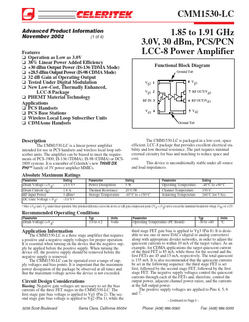
Features❏Operation as Low as 3.0V❏38% Linear Power Added Efficiency❏+30 dBm Output Power (IS-136 TDMA Mode) ❏+28.5 dBm Output Power (IS-98 CDMA Mode)❏32 dB Gain at Operating Output ❏Tested Under Digital Modulation ❏New Low-Cost, Thermally Enhanced,LCC-8 Package❏PHEMT Material Technology Applications ❏PCS Handsets ❏PCS Base Stations❏Wireless Local Loop Subscriber Units ❏CDMAone Handsets DescriptionThe CMM1530-LC is a linear power amplifierintended for use in PCS handsets and wireless local loop sub-scriber units. The amplifier can be biased to meet the require-ments of PCS-1900, IS-136 (TDMA), IS-98 (CDMA) or DCS-1800 systems. It is a member of Celeritek’s new Triniti DX Pro ™family of 3V power amplifier MMICs.The CMM1530-LC is packaged in a low-cost, spaceefficient, LCC-8 package that provides excellent electrical sta-bility and low thermal resistance. The part requires minimal external circuitry for bias and matching to reduce space and cost.This device is unconditionally stable under all sourceand load impedances.1.85 to 1.91 GHz3.0V , 30 dBm, PCS/PCN LCC-8 Power AmplifierAdvanced Product Information November 2002(1 of 4)d g d g br Application InformationThe CMM1530-LC is a three stage amplifier that requires a positive and a negative supply voltages for proper operation.It is essential when turning on the device that the negative sup-ply be applied before the positive supply. When turning the device off, the positive supply should be removed before the negative supply is removed.The CMM1530-LC can be operated over a range of sup-ply voltages and bias points. It is important that the maximum power dissipation of the package be observed at all times and that the maximum voltage across the device is not exceeded.Circuit Design ConsiderationsBiasing Negative gate voltages are necessary to set the bias currents of the three FET stages in the CMM1530-LC. The first stage gate bias voltage is applied to Vg1 (Pin 2). The sec-ond stage gate bias voltage is applied to Vg2 (Pin 1), while thethird stage FET gate bias is applied to Vg3 (Pin 8). It is desir-able to use one or more DACs (digital to analog converters)along with appropriate divider networks, in order to adjust the quiescent currents to within 10 mA of the target values. As an example, for CDMA applications the target quiescent current of the third FET is 85 mA, while those for the second and the first FETs are 45 and 15 mA, respectively. The total quiescent is 135 mA. It is also recommended that the quiescent currents be set in the following sequence: the third stage FET is set first, followed by the second stage FET, followed by the first stage FET. The negative supply voltages control the quiescent currents through each of the FETs and, therefore, control the output power, adjacent channel power ratios, and the currents at the full output power.The positive supply voltages are applied to Pins 4, 5, 6and 7.– Continued on Page 2 –3236 Scott Boulevard, Santa Clara, California 95054ParameterConditionMinTypMaxUnitsFrequency Range 1.85 1.91GHz Gain@ Digital power output2831dB Gain Ripple*1805-1880 MHz & 1850-1910 MHz 1.5dB Gain VariationOver supply voltage 2dB/V Over temperature 0.03dB/°C Power Output Control Range Vdd = 0 V to +3.5 V50dB Power Output Meets IS-136 TDMA mask +30.0dBm Meets IS-98 CDMA mask+28.5dBm Harmonics2nd @ Digital power output, no output trapping, Po=+28.5 dBm -30dBc 3rd @ Digital power output, no output trapping, Po=+28.5 dBm -40dBc Noise Power in Receive Band 30 kHz bandwidth-94dBmLinearityCDMA modulation @ +28.5 dBm Pout, 1.25 MHz offset -45dBc/30KHz TDMA modulation @ +30 dBm Pout - Adjacent -26dBc TDMA modulation @ +30 dBm Pout - Alternate -45dBc Spurious Signal VSWR = 3:1 in-band, VSWR = 10:1 out-of-band-80dBc Noise Figure3.0dB Input Return Loss 10dB Output Return Loss 8dB Efficiency (Vdd = 3.0 V)Pout = +30.0 dBm - TDMA 3638%Pout = +28.5 dBm - CDMA 3235%Positive Supply Current (I d )Pout IS-136 TDMA 750mA Pout IS-98 CDMA 595mA Quiescent Current (I q )No RF CDMA mode 130mA No RF TDMA mode200mA Negative Supply Current (-I g )Includes external resistor divider 1.1 2.0mA Negative Supply Voltage (-V g )Into external resistor divider-0.5-0.8-1.4VElectrical CharacteristicsUnless otherwise specified, the following specifications are guaranteed at room temperature with drain voltage (+V d ) = 3.5 V in Celeritek test fixture.* Specifications guaranteed over the temperature range of -20°C to +80°C(3 of 4)IS-98 CDMA Spectral Mask(Vdd=3.5V, 1,880 MHz, Po=+28.5 dBm)TDMA Power Output and Efficiency vs Input Power(3.0V, 1.91 GHz)Input Output, dBm0152535-13-117.5-10-7-452.535.0A d j a c e n t C h a n e l Id & IS-136 TDMA ACPR vs Power Output (3.5V, 1.91 GHz)-6020060010001930-40-20Adjacent channel power (worst case, Fc ±30 kHz)Alternate channel power (worst case, Fc ±60 kHz)21.7524.527.25Power Output, dBm (30 kHz BW)IdId & IS-98 CDMA ACPR vs Power Output (3.5V, 1.91 GHz)Power Output, dBm (1.25 MHz BW)-55100400800-50-45Adjacent channel power (worst case ±1.25 MHz)28.57.12514.521.625CDMA Power Output, 2nd and 3rd Harmonicsvs Input Power (3.5V, 1.91 GHz)Input Output, dBm-60152535-26.5-2.5-45P o w e r O u t p u t , d B m5-20.5-14.5-8.5-302nd3rd(Vdd=3.5V, 1,752 MHz, Po=+28.5 dBm)3236 Scott Boulevard, Santa Clara, California 95054Physical DimensionsRecommended Matching TopologyNote: This schematic represents the topology of the matching circuit recommended by Celeritek.Evaluation Board SchematicER = 4.60Thickness = 0.031 in.cc TXRF OUTRF IN 1.5 K 65V 元器件交易网。
涓流充电计时芯片DS1302中文手册
I特性★实时时钟计算年、月、日、时、分、秒、星期,直到 2100 年,并有闰年调节功能★31 x 8 位 通用暂存 RAM ★串行输入输出使管脚数最少★ 2.0V 至 5.5V 宽电压范围操作★在 2.0V 时工作电流小于 300nA★读写时钟或 RAM 数据时有单字节或多字节(脉冲串模式)数据传送方式★8 管脚 DIP封装或可选的 8 管脚表面安装 SO 封装★简单的 3 线接口★与 TTL 兼容 (VCC = 5V)★可选的工业温度范围:-40°C to +85°C ★与 DS1202 兼容★美国保险商试验室(UL®)认证订货信息型号温度范围管脚封装顶端标志+表示无铅/符合RoHS 标准的封装.*顶端标识上的N 表示工业温度范围器件,A 表示无铅器件. UL 是美国保险商试验室的注册商标.详细描述DS1302涓流充电计时芯片包含一个实时时钟/日历和31字节的静态RAM.通过简单的串行接口与微处理器通讯.这个实时时钟/日历提供年月日,时分秒信息.对于少于31天的月份月末会自动调整,还有闰年校正.由于有一个AM/PM 指示器,时钟可以工作在12小时制或者24小时制。
使用同步串行通讯简化了DS1302与微处理器的接口。
与时钟/RAM 通讯只需要三根线: CE, I/O (数据线), and SCLK (串行时钟). 数据输出输入时钟/RAM 一次1字节或者在脉冲串中多管脚定义D S 1302涓流充电计时芯片达31字节. DS1302被设计工作在非常低的电能下,在低于1μW 时还能保持数据和时钟信息. DS1302是DS1202的后继者. 除了DS1202的基本计时功能以外, DS1302有额外特点比如,双管脚主电源和备用电源,可编程涓流充电器V CC1,还附加7字节的暂存器.操作图1显示了串行计时器的主要元素:移位寄存器,控制逻辑,振荡器,实时时钟,还有RAM.典型工作电路图1框图: 典型工作性能(V C C = 3.3V , T A = +25°C ,除非另外声明.)电源控制输入移位寄存器命令控制逻辑实时时钟管脚描述管脚 名称 功能1V CC2双供电配置中的主电源供应管脚,V CC1连接到备用电源,在主电源失效时保持时间和日期数据.D S1302工作于V CC1和V CC2中较大者.当V CC2比V CC1高0.2V时,V CC2 给 D S1302供电.当V CC1比V CC2高时, V CC1给D S1302供电.2X1 3X2与标准的32.768k H z石英晶体相连.内部振荡器被设计与指定的6p F 装载电容的晶体一起工作.更多关于晶体选择和布局注意事项的信息请参考应用笔记58页:D a l l a s实时时钟晶振注意事项.D S1302也可以被外部的32.768k H z振荡器驱动.这种配置下,X1与外部震荡信号连接,X2悬浮.4G N D电源地5C E输入.C E信号在读写时必须保持高电平.此管脚内部有一个40kΩ(典型值)的下拉电阻连接到地.注意:先前的数据手册修正把C E当作R S T.管脚的功能没有改变.6I/O输入/推挽输出.I/O管脚是三线接口的双向数据管脚.此管脚内部有一个40kΩ(典型值)的下拉电阻连接到地.7S C L K输入.S C L K用来同步串行接口上的数据动作.此管脚内部有一个40kΩ(典型值)的下拉电阻连接到地.8V CC1低功率工作在单电源和电池工作系统和低功率备用电池.在使用涓流充电的系统中,这个管脚连接到可再充能量源.U L认证在使用锂电池时确保避免反向充电电流.振荡电路D S1302使用一个外部32.768k H z晶体.振荡电路工作时不需要任何外接的电阻或者电容表1 详细指明了几个外部晶体的参数.图1 显示了震荡电路的功能简图.如果使用指定规格的晶体,启动时间通常少于1秒钟.时钟精确度时钟的精确度取决于晶振的精确度,以及振荡电路容性负载与晶振校正的容性负载之间匹配的精确度。
SAT31技术说明书(3.00) 2011-02-17
SAT31测控保护装置技术说明书(3.00)-2011年1月-•装置的操作使用,请参见《产品使用手册》。
•本说明书的内容:1. SAT31概述 (1)SAT31装置概述2. SAT31-2变压器测控保护装置 (11)SAT31-2功能说明3. SAT31-3变压器测控保护装置 (42)SAT31-3功能说明4.附录A 插件E的配置应用 (69)5.附录B 插件B的配置应用 (73)6.附录C 插件F的配置应用 (75)7.附图概述SAT31测控保护装置适用于110kV及以下电压等级变压器单侧的后备保护及测量、控制,可满足保护及远动双重标准的要求。
1.1功能配置功能SAT31-2 SAT31-3过流保护◆◆过流复压闭锁◆◆过流方向闭锁◆过负荷◆◆过负荷启动风冷◆过负荷闭锁调压◆零序过流保护◆◆间隙零流保护(或小电阻零流)◆零序过压保护◆非电量保护◆◆低电压保护◆断线判别◆◆母线保护(充电保护/ 简易保护)◆故障录波◆◆变压器单侧测控◆◆可接打印机◆注:◆表示该型号装置具备此功能。
1.2技术数据1.2.1. 额定参数装置电源直流220V或110V(订货时请注明)交流电压100V交流电流5A或1A(订货时请注明)额定频率50Hz功率消耗直流电源回路:正常工作时,不大于25W;保护动作时,不大于30W交流电流回路:额定5A时每相不大于0.75VA;额定1A时每相不大于0.5VA交流电压回路:每相不大于0.5VA1.2.2. 性能参数交流量测量精度电压、电流:±0.2%功率及因数:±0.5%频率:±0.01Hz过载能力测控电流回路:1.2倍额定电流时,连续工作;20倍额定电流时,允许1s保护电流回路:2倍额定电流时,连续工作;10倍额定电流时,允许10s;40倍额定电流时,允许1s交流电压回路:1.2倍额定电压时,连续工作;1.4倍额定电压时,允许10s;2倍额定电压时,允许1s直流电源回路:0.8~1.2倍的额定电压时,连续工作(装置经受过载电流/电压后,无绝缘损坏,装置性能不下降)开关量采集信号电平:直流220V或110V或24V(订货时请注明)接入方式:无源空接点SOE站内分辨率:不大于2ms脉冲量采集信号电平:直流24V脉冲要求:宽度应不小于5ms;脉冲周期不小于50ms接入方式:无源空接点或有源脉冲保护精度电流精度:±3%或±0.02 In电压精度:±3%或±0.001 Un角度精度:±5°动作时间:零时限时不大于40ms;定时限时,±2%或±30ms出口接点容量直流220V,5A,不允许断弧绝缘性能绝缘电阻:符合DL/T478-2001中4.10.2和GB/T13729-2002中3.6.1的规定介质强度:符合DL/T478-2001中4.10.3和GB/T13729-2002中3.6.2的规定冲击电压:符合DL/T478-2001中4.10.4和GB/T13729-2002中3.6.3的规定电磁兼容性能辐射电磁场:装置能承受GB/T17626.3-1998中规定的试验等级为Ⅲ级的试验脉冲群干扰:装置能承受GB/T14598.13-1998规定的严酷等级为Ⅲ级的1MHz及100KHz试验浪涌:装置能承受GB/T17626.5-1999中规定的试验等级为Ⅳ级的试验快速瞬变:装置能承受GB/T14598.10-1996中规定的严酷等级为Ⅳ级的试验静电放电:装置能承受GB/T14598.14-1998中规定的严酷等级为Ⅳ级的试验射频传导:装置能承受GB/T17626.6-1998中规定的严酷等级为Ⅲ级的射频传导干扰试验工频干扰:装置能承受IEC60255-22-7:2003中规定的严酷等级为A级的工频干扰试验工频磁场:装置能承受GB/T17626.8-1998中规定的试验等级为Ⅴ级的工频磁场干扰试验脉冲磁场:装置能承受GB/T17626.9-1998中规定的严酷等级为Ⅳ级的脉冲磁场干扰试验传导发射:传导发射限值满足GB/T14598.16-2002中的规定机械性能 振动响应:装置能承受GB/T11287-2000中3.2.1规定的严酷等级为1级的振动响应试验振动耐久:装置能承受GB/T11287-2000中3.2.2规定的严酷等级为1级的振动耐久试验冲击响应:装置能承受GB/T14537-1993中4.2.1规定的严酷等级为1级的冲击响应试验冲击耐久:装置能承受GB/T14537-1993中4.2.2规定的严酷等级为1级的冲击耐久试验碰撞: 装置能承受GB/T14537-1993中4.3规定的严酷等级为1级的碰撞试验1.3 装置显示及操作装置的液晶和键盘操作的详细说明,请参见《产品使用手册》。
MAXIM DS3231 说明书
_________________________________概述DS3231是低成本、高精度I 2C 实时时钟(RTC),具有集成的温补晶体振荡器(TCXO) 和晶体。
该器件包含电池输入端,断开主电源时仍可保持精确的计时。
集成晶体振荡器提高了器件的长期精确度,并减少了生产线的元件数量。
DS3231提供商用级和工业级温度范围,采用16引脚、300mil 的SO 封装。
RTC 保持秒、分、时、星期、日期、月和年信息。
少于31天的月份,将自动调整月末日期,包括闰年补偿。
时钟的工作格式可以是24小时或带AM /PM 指示的12小时格式。
提供两个可编程日历闹钟和一路可编程方波输出。
地址与数据通过I 2C 双向总线串行传输。
精密的、经过温度补偿的电压基准和比较器用来监视V CC 状态,检测电源故障、提供复位输出,并在必要时自动切换到备用电源。
另外,RST 监视引脚可以作为手动按钮输入以产生外部复位信号。
_________________________________应用服务器电表远程信息处理系统GPS_________________________________特性♦0°C 至+40°C 范围内精度为±2ppm ♦-40°C 至+85°C 范围内精度为±3.5ppm ♦为连续计时提供备用电池输入♦工作温度范围商用级:0°C 至+70°C 工业级:-40°C 至+85°C♦低功耗♦实时时钟提供秒、分、时、星期、日期、月、年信息,并提供有效期到2100年的闰年补偿♦两个日历闹钟♦可编程方波输出♦快速(400kHz) I 2C 接口♦3.3V 工作电压♦数字温度传感器输出:精度为±3°C ♦老化修正寄存器♦RST 输入/输出DS3231高精度、I 2C 集成RTC/TCXO/晶体______________________________________________Maxim Integrated Products1Rev 1; 2/05______________________________定购信息引脚配置在数据资料的最后部分给出。
ST串行实时时钟(RTC)应用指南AN3060说明书
2015年11月DocID16253 Rev 1 [English Rev 3] 1/25 AN3060 应用笔记串行实时时钟(RTC )应用指南 Doug Sams前言ST 串行实时时钟(RTC )系列产品广受用户欢迎。
多年来,关于这些器件的许多问题已被支持它们的应用程序组解决了。
本文档汇集了一些已解决的最普遍问题,包括晶振的布线考虑到上电时正确的软件访问。
这会帮助读者理解RTC 的一些精微之处,以及怎样保持其可靠运行。
AN3060 目录目录1电池连接和充电保护 (5)1.1串联电阻 (5)1.2电池上的去耦电容 (5)1.3阻断二极管 (6)1.4面向ST实时时钟的Underwriters Laboratories文件 (6)1.5电池安装 (7)2布局考虑 (8)2.1RTC晶振的某些基本布局考虑是什么? (8)3振荡器电路 (9)3.1除了晶振之外,还需要添加什么其他元件来使RTC振荡器正确工作? (9)4负超调 (11)4.1负超调会影响我的实时时钟工作吗?如何影响?如何防止该影响? 11 5切换电压 (12)5.1切换电压是否依赖于电池电平?或者它始终是一个固定值?RTC的最大电池电压是多少? (12)6振荡器失效检测 (15)6.1什么是OF位?它如何工作? (15)7电池低电平检测 (16)7.1电池低电平位是如何工作的?它能检测缺失的电池吗? (16)8挂起(HT)位 (18)8.1挂起位(HT)有什么作用?如何使用它? (18)9RTC初始化 (21)9.1初次上电时访问RTC的最佳时序是什么?后续上电呢? (21)10版本历史 (24)DocID16253 Rev 1 [English Rev 3] 2/25表格索引表1:取消选择和切换阈值总结 (13)表2:M41T81S寄存器映射 (16)表3:M41ST85W寄存器映射 (18)表4:文档版本历史 (24)表5:中文文档版本历史 (24)DocID16253 Rev 1 [English Rev 3] 3/25图表索引图1:RTC/NVRAM中的电池切换电路 (5)图2:VBAT通路上二极管的影响 (6)图3:SNAPHAT SOIC封装 (6)图4:带有固定片的钮扣电池 (7)图5:布局考虑 (8)图6:内置负载电容 (9)图7:典型寄生二极管 (11)图8:负超调保护 (11)图9:典型切换电路 (12)图10:切换电路 (13)图11:振荡器失效检测电路 (15)图12:电池监测功能 (17)图13:时钟和非时钟寄存器 (19)图14:M41T83/M41T82上电默认值 (21)图15:初次上电 (22)图16:从备份上电 (23)DocID16253 Rev 1 [English Rev 3] 4/251 电池连接和充电保护ST串行实时时钟的电池连接非常简单。
- 1、下载文档前请自行甄别文档内容的完整性,平台不提供额外的编辑、内容补充、找答案等附加服务。
- 2、"仅部分预览"的文档,不可在线预览部分如存在完整性等问题,可反馈申请退款(可完整预览的文档不适用该条件!)。
- 3、如文档侵犯您的权益,请联系客服反馈,我们会尽快为您处理(人工客服工作时间:9:00-18:30)。
北京周立功
重庆周立功
地址:北京市海淀区知春路 113 号银网中心 712 室 地址:重庆市石桥铺科园一路二号大西洋国际大厦
(中发电子市场斜对面)
(赛格电子市场)1611 室
电话:(010)62536178 62536179 82628073
电话:(023)68796438 68796439
传真:(010)82614433
7.1 后备电源供电....................................................................................................................4 7.2 涓流充电器........................................................................................................................5 7.3 校准....................................................................................................................................5 7.4 晶振类型............................................................................................................................5 7.5 布线注意事项....................................................................................................................6 7.6 警报器................................................................................................................................8 7.7 ACS 引脚的功能 ................................................................................................................9 7.8 校准输出/方波输出...........................................................................................................9 8. 寄存器映射................................................................................................................................10 8.1 寄存器映射一览表..........................................................................................................10 9. 寄存器描述................................................................................................................................ 11 9.1 地址描述.......................................................................................................................... 11 10. 双线接口..................................................................................................................................14 10.1 开始状态........................................................................................................................14 10.2 停止状态........................................................................................................................14 10.3 数据/地址传输...............................................................................................................14 10.4 答应................................................................................................................................15 10.5 从机地址........................................................................................................................15 10.6 寻址概述——存储器....................................................................................................15 10.7 寻址概述——RTC/警报器 ...........................................................................................16 10.8 数据传输........................................................................................................................16 10.9 存储器写操作................................................................................................................16 10.10 存储器读操作..............................................................................................................17
海纳电子资讯网www.fpga-arm.com为您提供各种IC的应用资料
广州周立功单片机发展有限公司
技术支持
如果您对文档有所疑问,您可以在办公时间(星期一至星期五上午 8:30~11:50;下午 1:30~5:30;星期六上午 8:30~11:50)拨打技术支持电话或 E-mail 联系。
网 址: 联系电话: +86 (020) 22644358 22644359 22644360 22644361 E-mail: zlgmcu.support@
广州周立功单片机发展有限公司
目录
目录
1. 特性..............................................................................................................................................1 2. 概述..............................................................................................................................................1 3. 引脚配置......................................................................................................................................2 4. 引脚描述......................................................................................................................................3 5. 简述..............................................................................................................................................3 6. 存储器操作..................................................................................................................................3 7. 实时时钟操作..............................................................................................................................4