A single-inductor dual-output buck converter with self-adapted PCCM method
电力电子术语中英文对照
电力电子技术术语Absorber Circuit 吸收电路AC/ACFrequency Converter 交交变频电路AC power control 交流电力控制AC Power Controller 交流调功电路AC Power Electronic Switch 交流电力电子开关AC Voltage Controller 交流调压电路Asynchronous Modulation 异步调制Baker Clamping Circuit 贝克箝位电路Bi—directional Triode Thyristor 双向晶闸管Bipolar Junction Transistor——BJT 双极结型晶体管Boost—Buck Chopper 升降压斩波电路Boost Chopper 升压斩波电路Boost Converter 升压变换器Bridge Reversible Chopper 桥式可逆斩波电路Buck Chopper 降压斩波电路Buck Converter 降压变换器Commutation 换流Conduction Angle 导通角Constant Voltage Constant Frequency-—CVCF恒压恒频Continuous Conduction——CCM (电流)连续模式Control Circuit控制电路CUK Circuit CUK 斩波电路Current Reversible Chopper 电流可逆斩波电路Current Source Type Inverter——CSTI 电流(源)型逆变电路Cycloconvertor 周波变流器DC-AC-DC Converter 直交直电路DC Chopping 直流斩波DC Chopping Circuit直流斩波电路DC-DC Converter 直流-直流变换器Device Commutation 器件换流Direct Current Control 直接电流控制Discontinuous Conduction mode (电流)断续模式Displacement Factor 位移因数Distortion Power 畸变功率Double End Converter 双端电路Driving Circuit 驱动电路Electrical Isolation 电气隔离Fast Acting Fuse 快速熔断器Fast Recovery Diode 快恢复二极管Fast Recovery Epitaxial Diodes 快恢复外延二极管Fast Switching Thyristor 快速晶闸管Field Controlled Thyristor 场控晶闸管Flyback Converter 反激电流Forced Commutation 强迫换流Forward Converter 正激电路Frequency Converter 变频器Full Bridge Converter 全桥电路Full Bridge Rectifier 全桥整流电路Full Wave Rectifier 全波整流电路Fundamental Factor 基波因数Gate Turn—Off Thyristor—-GTO可关断晶闸管General Purpose Diode 普通二极管Giant Transistor—-GTR 电力晶体管Half Bridge Converter 半桥电路Hard Switching 硬开关High Voltage IC 高压集成电路Hysteresis Comparison 带环比较方式Indirect Current Control 间接电流控制Indirect DC-DC Converter 直接电流变换电路Insulated—Gate Bipolar Transistor--IGBT 绝缘栅双极晶体管Intelligent Power Module——IPM 智能功率模块Integrated Gate—Commutated Thyristor——IGCT集成门极换流晶闸管Inversion 逆变Latching Effect 擎住效应Leakage Inductance 漏感Light Triggered Thyristo--—LTT 光控晶闸管Line Commutation 电网换流Load Commutation 负载换流Loop Current 环流元件设备三绕组变压器:three-column transformer ThrClnTrans双绕组变压器:double-column transformer DblClmnTrans 电容器:Capacitor并联电容器:shunt capacitor电抗器:Reactor母线:Busbar输电线:TransmissionLine发电厂:power plant断路器:Breaker刀闸(隔离开关):Isolator分接头:tap电动机:motor状态参数有功:active power无功:reactive power电流:current容量:capacity电压:voltage档位:tap position有功损耗:reactive loss无功损耗:active loss功率因数:power—factor功率:power功角:power-angle电压等级:voltage grade空载损耗:no—load loss铁损:iron loss铜损:copper loss空载电流:no-load current阻抗:impedance正序阻抗:positive sequence impedance 负序阻抗:negative sequence impedance 零序阻抗:zero sequence impedance电阻:resistor电抗:reactance电导:conductance电纳:susceptance无功负载:reactive load 或者QLoad有功负载: active load PLoad遥测:YC(telemetering)遥信:YX励磁电流(转子电流):magnetizing current 定子:stator功角:power-angle上限:upper limit下限:lower limit并列的:apposable高压: high voltage低压:low voltage中压:middle voltage电力系统power system发电机generator励磁excitation励磁器excitor电压voltage电流current母线bus变压器transformer升压变压器step-up transformer高压侧high side输电系统power transmission system输电线transmission line固定串联电容补偿fixed series capacitor compensation 稳定stability电压稳定voltage stability功角稳定angle stability暂态稳定transient stability电厂power plant能量输送power transfer交流AC装机容量installed capacity电网power system落点drop point开关站switch station双回同杆并架double—circuit lines on the same tower 变电站transformer substation补偿度degree of compensation高抗high voltage shunt reactor无功补偿reactive power compensation故障fault调节regulation裕度magin三相故障three phase fault故障切除时间fault clearing time极限切除时间critical clearing time切机generator triping高顶值high limited value强行励磁reinforced excitation线路补偿器LDC(line drop compensation)机端generator terminal静态static (state)动态dynamic (state)单机无穷大系统one machine - infinity bus system 机端电压控制AVR电抗reactance电阻resistance功角power angle有功(功率)active power无功(功率)reactive power功率因数power factor无功电流reactive current下降特性droop characteristics斜率slope额定rating变比ratio参考值reference value电压互感器PT分接头tap下降率droop rate仿真分析simulation analysis传递函数transfer function框图block diagram受端receive-side裕度margin同步synchronization失去同步loss of synchronization 阻尼damping摇摆swing保护断路器circuit breaker电阻:resistance电抗:reactance阻抗:impedance电导:conductance电纳:susceptance导纳:admittance电感:inductance电容: capacitance一般术语电力电子变流器的型式(表1—2)电力电子开关和交流电力电子控制器电力电子设备的基本元件电力电子设备的电路和电路单元电力电子设备的运行电力电子设备的性能电力电子变流器的特性曲线稳定电源。
单相Boost_APFC电路的设计与分析
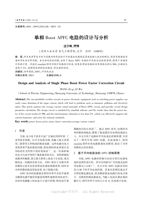
文章编号:1004-289X(2021)06-0055-03单相BoostAPFC电路的设计与分析汪子琦ꎬ厉伟(沈阳工业大学电气工程学院ꎬ辽宁㊀沈阳㊀110870)摘㊀要:开关电源等电力电子设备内部存在的不可控整流电路很容易造成输入电流的畸变ꎬ将会导致谐波污染和用电安全等问题ꎮ本文针对这些问题ꎬ分析了BoostAPFC电路的平均电流法控制原理ꎬ提供了电路设计参数计算ꎮ并通过simulink软件对设计电路进行仿真ꎬ结果表明该电路的功率因数达到0 996ꎬ总谐波失真低于2%ꎬ能够有效抑制电流谐波ꎬ符合国家标准ꎮ关键词:功率因数ꎻAPFCꎻ平均电流法中图分类号:TM13㊀㊀㊀㊀㊀文献标识码:BDesignandAnalysisofSinglePhaseBoostPowerFactorCorrectionCircuitWANGZi ̄qiꎬLIWei(SchoolofElectricEngineeringꎬShenyangUniversityofTechnologyꎬShenyang110870ꎬChina)Abstract:Theuncontrollablerectifiercircuitsinpowerelectronicequipmentsuchasswitchingpowersuppliescaneasilycausedistortionoftheinputcurrentꎬwhichwillleadtoproblemssuchasharmonicpollutionandelectricitysafety.ThisarticleanalyzestheaveragecurrentcontrolprincipleofBoostAPFCcircuitꎬandprovidescircuitdesignparametercalculation.Thedesigncircuitissimulatedbysimulinksoftwareꎬandtheresultsshowthatthepowerfac ̄torofthecircuitreaches0 996ꎬandthetotalharmonicdistortionislessthan2%ꎬwhichcaneffectivelysuppressthecurrentharmonicsandmeetthenationalstandards.Keywords:powerfactorꎻactivepowerfactorcorrectionꎻaveragecurrentcontrol1㊀引言目前ꎬ电力电子技术日益广泛地应用到军事㊁工业等技术领域ꎮ以开关电源为例ꎬ其输入级大多利用二极管等元件构成的整流电路ꎮ这些电路为电力系统带来严重的谐波问题ꎬ使电网的供电质量以及用电的安全性得不到有效保证[1]ꎮ这一负面影响在电力行业中得到了越来越多的关注ꎮ如何抑制电流脉冲的幅值ꎬ使之最大程度上接近于正弦波ꎬ成为解决这一问题的有效方法ꎮAPFC相比于无源功率因数校正技术有更加明显的谐波抑制效果ꎬ同时对功率因数的提高更加显著㊁抗干扰能力强ꎮ㊀㊀APFC技术的思路就是利用功率开关的开通和关断将电感中储存的能量周期性地释放到电容中ꎬ从而对电路输入的电流大小进行控制ꎬ使电流尽量跟随电压的正弦波[2]ꎮ通过APFC技术ꎬ电源的功率因数得到提高ꎬ降低了整流器件对电网的谐波注入ꎮ本文介绍了电路的平均电流法控制原理ꎬ并设计了一种升压型APFC电路ꎮ在此基础上ꎬ利用simulink软件对该电路搭建仿真模型ꎬ验证了功率因数校正的有效性ꎮ2㊀基于平均电流法的APFC控制原理㊀㊀目前ꎬAPFC电路的控制方法的分类以电感电流的连续性进行的ꎮ其中应用最为广泛的就是连续导电模式(CCM)[3]ꎮ本文中的APFC电路采用的是CCM下的平均电流控制ꎮ其基本原理是通过开关管控制电感电流ꎬ使其跟踪整流电路后的电压指令ꎮ具体的控制思路就是ꎬ当输入电流比乘法器的输出大ꎬ调节功率开关的占空比Dꎬ从而减小电流ꎮ反之当输入电流的有效值小于乘法器的输入信号时ꎬ则增大电流ꎮ这样输入电流和输入电压同相位ꎮ避免了整流元件对电网的谐波注入ꎬ提升能源效率ꎮ图1为平均电流法BoostAPFC电路图ꎮ其控制回路分为电流环和电压环ꎮ在连续电流模式下ꎬ电路工作时电感电流波形图如图2所示ꎮ图1㊀平均电流法BoostAPFC电路图图2㊀电感电流波形图3㊀BoostAPFC电路的设计3 1㊀电路的技术指标㊀㊀BoostAPFC电路在开关电源等电子装置中应用极为广泛ꎮ一方面能够实现功率因数校正的目的ꎬ另一方面也能稳定输出直流电压ꎬ其控制较简单适用中小功率电源中[4]ꎮ本文设计的BoostAPFC电路主要技术指标如表1所示ꎮ表1㊀BoostAPFC电路的技术指标序号参数数值1输入电压范围Uin180~260V2工作频率fN50Hz3输出直流电压U0400V4开关频率fsw100kHz5输出功率P600W6功率因数cosφ>0 993 2㊀升压电感计算㊀㊀Boost电路的升压电感的在电路中有储能㊁转换和滤波的作用ꎮ输入电压为最小(180V)ꎬ此时输入电流达到最大ꎮ按照表1的参数计算电流峰值:㊀㊀Ipk==2PUin(min)=5.12A(1)㊀㊀输入电流的纹波和电感的大小有着非常密切的关系ꎮ过大的电感能够有效降低纹波ꎬ但是也带来了电感尺寸的增大和成本的提升ꎬ不符合电源的小型化原则[5]ꎮ根据工程实践的经验ꎬ一般情况下电流的纹波系数取0 2ꎮ可以计算出电流纹波为:㊀㊀ΔIL=0 2Ipk=1 024A(2)㊀㊀此时电路的占空比为:㊀㊀D=U0-2Uin(min)U0=0 36(3)㊀㊀计算得出升压电感为:㊀㊀L=2Uin(min)ˑDΔIL=894 54μH(4)3 3㊀输出电容计算㊀㊀在BoostAPFC电路中输出电容可以降低纹波ꎬ稳定输出电压[6]ꎮ工程实践中一般采用按照维持时间Δt来计算ꎬ本电路的输出电容为:㊀㊀C=2PΔtU20-U20(min)=514μF(5)4㊀单相BoostAPFC电路的仿真分析㊀㊀为了验证本文所设计的BoostAPFC电路是否符合理论性和国家标准ꎬ利用MATLAB搭建出仿真模型ꎮ主回路的具体参数由第二部分计算得出ꎮ控制回路分为电流内环和电压外环ꎮ仿真模型整体如图3所示ꎮ图3㊀BoostAPFC电路仿真模型㊀㊀输出电压的仿真结果可以验证电路的输出稳定性ꎮ图4为输出直流电压的波形图ꎬ可以看出电路启动时电压的最大值为420V左右ꎬ超调量为5%ꎬ之后很快达到了稳态ꎬ电压值为设计的400Vꎮ本电路的纹波电压不超过 ʃ8V ꎬ满足纹波率不超过2%的设计指标ꎮ图4㊀BoostAPFC电路输出电压波形㊀㊀图5为输入交流电压㊁电流的波形图ꎬ可以看出当电路达到稳定状态时ꎬ输入电流㊁电压的相位基本相同ꎬ提高功率因数ꎬ达到了电路的工作目的ꎮ图5㊀BoostAPFC电路输入波形图6㊀BoostAPFC电路的功率因数变化曲线㊀㊀通过Power模块可以得到输入的有功功率和无功功率ꎬ搭建函数模块可以计算出cosφ的数值ꎮ图6为电路输入电流的功率因数cosφ变化曲线ꎮ由图可知ꎬ当电路处于刚开始的波动时ꎬ功率因数已经达到了0 996以上ꎻ电路处于稳定的状态时ꎬ功率因数大于0 999ꎮ在实际的APFC电路中可能有所降低ꎬ但是依然能够满足国家标准的要求ꎮ㊀㊀快速傅里叶变换(FFT)在数字处理领域是许多数字信号处理方法的基础[7]ꎮ通过FFT工具箱析输入电流ꎮ图7为仿真结果ꎬTHD仅为1 9%ꎬ满足设计标准ꎮ图7㊀输入电流的FFT分析频谱5㊀结论㊀㊀针对整流器件对电网产生的谐波污染问题ꎬ本文分析APFC电路在CCM下的平均电流控制原理ꎬ并设计了BoostAPFC电路ꎮ针对设计的电路搭建模型进行仿真ꎬ该电路能够将功率因数提升至0 996ꎬ总谐波失真为1 9%ꎬ符合国家标准ꎮ参考文献[1]㊀李明ꎬ莘炜杰ꎬ于千越ꎬ等.基于抗饱和积分的APFC仿真研究[J].通信电源技术ꎬ2021ꎬ38(1):14-17.[2]㊀王兆安ꎬ刘进军ꎬ电力电子技术[M].北京:机械工业出版社ꎬ2009:224-227.[3]㊀CanalesFꎬEscobarG.OlmosAꎬetal.Achargecontrolforinter ̄leavedoperationofaPFCboostconverter.IEEEInternationalSymposiumonIndustrialElectronics.IEEEꎬ2010:2987-2992.[4]㊀沈黎韬.CCM模式有源功率因数校正技术的研究[D].苏州大学ꎬ2018.[5]㊀LiuxSꎬXuJPꎬChenZYꎬetal.Single ̄inductordual ̄outputbuck ̄boostpowerfactorcorrectionconverter[J].IEEETransactionsonIndus ̄trialElectronicsꎬ2015ꎬ62(2):943-952.[6]㊀马鹏飞.基于平均电流法的单相Boost功率因数校正系统研究[D].华中科技大学ꎬ2018.[7]㊀FukaishiYꎬHiguchiKꎬFuruyaHꎬetal.DesignofrobustdigitalcontrollerforinterleavePFCboostconverterwithDC-DCconverterload.IEEEInternationalConferenceonElectronDevicesandSolidStateCircuit.IEEEꎬ2013:1-2.收稿日期:2021-07-26。
UPS中CLA协同控制双Buck逆变器设计

UPS中CLA协同控制双Buck逆变器设计陈裕成;卢德祥;王武【摘要】In view of the high reliability requirement of the UPS (uninterrupted power supply) to the inverter circuit,and the conventional DSP with single core in the UPS is difficult to implement the functions of detection,protection,communication and current converter.A design scheme of UPS system with high reliability by using the DSP CLA (control law accelerator) is processed.The topology structure of dual-buck inverter is adopted to improve the reliability of the inverter;through the analysis of the UPS circuit topology and the operating principles of the dual-buck inverter,and using the TMS320F28069 DSP with the CLA sharing the functions of the UPS' s task,and can achieve the UPS system without additional DSP.Finally,the feasibility of the design method is verified a 1 kW experimental prototype.%不间断电源(UPS)对逆变环节的可靠性要求高,UPS系统中DSP需承担检测、保护、通讯和变流等功能,传统单核DSP难以适用.为此,提出一种运用内嵌控制律加速器(CLA)的DSP控制高可靠性的UPS系统设计方案.逆变环节采用双Buck拓扑结构提高可靠性;通过对UPS主电路拓扑和双Buck逆变工作原理分析,运用DSP TMS320F28069的CLA功能分担系统任务进行协同控制,不需增加额外的DSP,实现UPS系统设计.最后通过一台1 kW的实验样机,验证设计方法的可行性.【期刊名称】《福州大学学报(自然科学版)》【年(卷),期】2018(046)001【总页数】6页(P89-94)【关键词】双Buck逆变器;CLA;高可靠性;UPS【作者】陈裕成;卢德祥;王武【作者单位】漳州职业技术学院建筑工程系,福建漳州363000;福州大学电气工程与自动化学院,福建福州350116;福州大学电气工程与自动化学院,福建福州350116;福州大学电气工程与自动化学院,福建福州350116【正文语种】中文【中图分类】TM4640 引言逆变器作为新能源发电、航空供电和不间断电源(uninterrupted power supply,UPS)的关键设备,随着功率器件和变流技术的快速发展,国际能源变换对逆变器的可靠性和效率提出更高的要求[1]. 传统桥式逆变存在桥臂直通隐患,通常需增加软件或硬件死区防止桥臂共导,增加了软硬件成本;在续流阶段电流流经性能差的体二极管,限制变换效率和可靠性的提高[2]. 因此,无桥臂直通隐患、无开关管死区时间设计、可独立优化设计续流二极管的双Buck逆变电路成为高效、高可靠性逆变器的主要解决方案之一[3-4].双Buck逆变器的典型控制策略为滞环电流控制和正弦脉宽调制(sinusoidal pulse width modulation,SPWM)控制,滞环电流控制的双Buck逆变器具有动态响应速度快、电压电流过零处无波形畸变的优点,但其输出电压外特性软且输出谐波频谱宽、滤波器设计困难,不利于拓展成大功率三相双Buck运用; SPWM控制的双Buck逆变器设计便捷且系统的鲁棒性强,易于拓展成三相双Buck逆变运用[5]. 文献[6-7]分别在双环PI控制双Buck逆变器的基础上引入滑膜控制和谐振控制,提高双Buck逆变器输出波形质量和外特性. 多种控制策略组合的控制算法运用在双Buck逆变系统中可有效提高输出波形质量和外特性,但增加了中央处理器(CPU)的负担(特别在高频变换运用中);此外,采用高可靠性的双Buck逆变的UPS系统,主CPU任务包含功率因数校正(power factor correction,PFC)控制、孤岛检测、采样滤波和通讯控制等[8-10]. 传统方法实现UPS系统通常需要多片控制芯片完成,如文献[11]在AC-DC环节采用UC3854b芯片控制PFC,在DC-AC环节采用PIC16F870进行控制,DC-DC采用独立模拟芯片完成. 如何利用低成本、可市场化的数字信号处理器(digital signal processing,DSP)到UPS系统中,实现高频、高效、高可靠性的逆变方案,对数字化控制的双Buck逆变器在UPS的运用提出了挑战.本设计为双Buck逆变器组成的UPS系统,采用TI公司主频90 MHz的DSP TMS320F28069作为主控芯片,运用其内嵌控制律加速器(control law accelerator ,CLA)的功能,分担逆变控制和采样滤波程序,减轻主CPU的负担,使市电高频PFC控制、滤波、通讯监测和高频双Buck逆变等能在同一个DSP中实现,无需增加额外的DSP,降低系统设计成本.1 半周期控制双Buck工作原理分析1.1 双Buck逆变器工作原理图1 PFC升压电路和双Buck逆变器Fig.1 PFC Boost circuit and dual-buck inverter图1所示为前级PFC升压+双Buck逆变器构成的UPS系统,双Buck逆变器由两个Buck直流变换器组合而成,开关管S1、独立续流二极管D1和储能电感L1构成Buck电路1,因此左桥臂无直通路径,对应的Buck电路2的右桥臂也不存在直通路径,提高了逆变器的可靠性和效率.双Buck逆变全周期双极性调制无过零波形畸变问题,其工作模态见图2,在全周期调制模式下,Buck电路1和Buck电路2在整个周期内都调制工作.图2 工作模态Fig.2 Operating modes假设电路工作在理想条件,开关管S1的占空比为d1、周期为T,开关管S2与S1互补工作,电感L1和L2值为L,输出滤波电容值为C,开关管和二极管均为理想器件. 逆变器正半周工作时电感电流iL1>iL2.模态1 [0-d1T]:图2(a)中,Buck电路1工作,S1导通,S2断开,桥臂中点A的电位为Ud,电感L2的电流经开关管S1续流,输入电压与输出电压的差值施加在电感L1上,电感L1电流增加,变化率为:Ud-Uo=L(di/dt)(1)模态2 [d1T-T]:图2(b)中,S1断开,电感L1、 L2的电流均由二极管D1续流,桥臂中点A的电位为-Ud,在输入电压和输出电压的共同作用下电感L1的电流下降,变化率为:Ud+Uo=L(di/dt)(2)由电感的伏秒积平衡和式(1)、 (2)可得,输入与输出电压之间的关系式为:Uo=(2d1-1)Ud,正半周占空比表达式为:d1=0.5+(uo/2Ud)(3)逆变器负半周工作时电感电流iL1<iL2,此时开关管S2的占空比为d2,S1与S2互补工作,负半周电路工作模态如图2(c)、 (d)所示.模态3:如图2(c)所示,S1断开、S2闭合,Buck电路2工作,电感L1的电流经S2、D1续流,桥臂中点B的电位为-Ud,在输入电压和输出电压的共同作用下电感L2的电流上升,变化率为:-Ud+Uo=L(di/dt)(4)模态4:如图2(d)所示,S1导通,S2断开,桥臂中点B的电位为Ud,电感L1的电流经开关管S1和二极管D1续流,输入电压与输出电压的差值施加在电感L2上,此时电感L2电流增加,变化率为:-Ud-Uo=L(di/dt)(5)同理可得开关管S2的占空比表达式为:d2=0.5+(uo/2Ud)(6)现假设输入电压恒定,功率管均为理想器件,开关频率远高于输出LC滤波器的谐振频率,对阻性负载的双Buck电路建立小信号状态方程[7]为:(7)1.2 SPWM控制双Buck逆变图3 半周期SPWM控制系统Fig.3 SPWM control system with half cycle pulses采用双环SPWM控制的双Buck变换器具有快速动态响应和外特性硬的特点,且易于双Buck逆变器的并联实现三相输出,进一步提高逆变系统的容量和可靠性的特点. 图3为双Buck逆变器的半周期SPWM控制系统框图,控制结构由电压外环和电流内环构成,由式(7)可知双Buck变换器开环传递函数为:(8)其中: R为负载电阻; vref、 iref分别为参考电压和参考电流; V.PI和I.PI分别为电压、电流比例积分控制器,输出电压为vo,经过滤波后的反馈电压和电流值分别为vof、 iLf.2 DSP与CLA协同控制软件设计为实现PFC和逆变开关频率20 kHz工作,其余辅助功能均要在同一个DSP上实现,对于主频90 MHz的单核DSP很难完成. 选用TMS320F28069内嵌CLA功能的DSP,CLA与主CPU结合实现“伪双核”处理,能够有效分配运算任务,使复杂的控制系统能在低成本的DSP中实现,避免增加额外的DSP,降低UPS设计成本. 由双Buck逆变器和双向开关型无桥Boost PFC组成的在线式UPS系统软件流程图如图4所示.DSP的主CPU核负责PFC控制子程序、双向DC-DC变换控制子程序和捕获、定时器的管理;在线式UPS系统逆变环节在市电和停电环境下均需参与工作,若市电停电,主CPU会因掉电检测而执行中断子程序,而CLA可独立运行,由CLA负责双Buck逆变控制子程序可实时完成逆变任务,保证用电设备的稳定运行. 关键模块触发机制如图5所示,在CLA的中断触发机制上,利用逆变器模块对应的PWM1周期性触发CLA逆变子任务,任务完成后CLA将保持待命状态,直至下一个周期的PWM1中断触发.图4 UPS各模块在DSP中的分配Fig.4 Distribution of UPS’s modules in DSP图5 关键模块的触发机制Fig.5 Trigger mechanism of key modules3 仿真与实验测试应用PSIM软件与Microsoft Visual C++软件对UPS中逆变环节的SPWM控制双Buck逆变器进行联合仿真,系统参数如下:交流市电输入,经双向开关型无桥Boost PFC升压至直流母线电压为720 V;逆变环节直流输入电压为720 V,逆变器输出220 V/50 Hz交流电,开关频率fs=20 kHz,额定输出功率1 kW,阻性满载R=48 Ω,滤波电感值L=2.5 mH,滤波电容值C=12 μF. 图6为逆变环节带阻性负载时,输出电压uo、输出电流io和桥臂中点A处电压vAN的仿真波形.图6 双Buck逆变动静态仿真波形Fig.6 Static and dynamic simulation waveforms of dual-buck inverter为验证系统电路拓扑及控制策略的可行性,依据仿真参数搭建一台额定功率1 kW 前级由双向开关型无桥Boost PFC实现母线升压,后级为半桥型双Buck逆变器组成的在线式UPS系统,逆变环节阻性负载的实验波形如图7所示. 由仿真和实验波形可见,运用CLA协同控制的双极性SPWM调制双Buck逆变器具有动态响应速度快、无过零波形畸变和输出波形正弦度良好的特点.图7 双Buck逆变动静态实验波形Fig.7 Static and dynamic experimental waveforms of dual-buck inverterUPS逆变环节全周期调制的控制开关管S1和S2的驱动电压波形和逆变输出电压电流如图8(a)所示;在图8(a)中对应S1和S2的驱动电压波形在示波器高频展开时的工作模式如图8(b)所示,可见开关管S1和S2在整个周期都在参与工作,这种在电路的整个工作周期中S1和S2均参与工作的调制方式被称为双Buck逆变器的全周期调制;图8(c)为设计的UPS逆变输出带整流型负载的电压电流波形,可见双Buck逆变器采用电压单环控制,会引起输出电流畸变.图8 双Buck逆变驱动电压与带非线性负载实验波形 Fig.8 Experimental waveforms of dual-buck inverter driving voltage and nonlinear load图9(a)和(b)分别给出了逆变器输出带阻性负载时的效率、总谐波畸变(total harmonic distortion ,THD)随着输出功率增加变化的曲线图. 逆变器在输出功率900 W时存在峰值效率96%,满载输出时效率为95.7%;实验测试过程采用功率因数分析仪测量输出电压畸变,逆变输出在300 W以上时,实验测试的输出电压总谐波畸变保持在0.9%左右.图9 双Buck逆变效率及总谐波畸变曲线 Fig.9 Efficiency and total harmonic distortion of dual buck inverter4 结语运用主频90 MHz DSP TMS320F28069内嵌的CLA功能,无需增加额外的DSP 或集成控芯片,实现高可靠性的UPS系统设计. 运用DSP自带的CLA分担UPS中的逆变任务实现全周期SPWM调制的双Buck逆变器,所设计的逆变器具有良好的动静态性能. 此设计方法可降低软硬件成本,为高可靠性的UPS设计提供一种有效的解决方案.参考文献:[1] HONG F, LIU J, JI B, et al. Single inductor dual buck full-bridge inverter[J]. IEEE Transactions on Industrial Electronics, 2015, 62(8): 4869-4877.[2] 姚志垒, 肖岚, 魏星. 双降压全桥并网逆变器[J]. 中国电机工程学报, 2011,31(12): 29-33.[3] HONG F, LIU J, JI B, et al. Interleaved dual buck full-bridge three-level inverter[J]. IEEE Transactions on Power Electronics, 2016, 31(2): 964-974.[4] 洪峰, 刘周成, 万运强,等. 无漏电流高效可靠三电平双Buck并网逆变器[J]. 中国电机工程学报, 2014, 34(9): 1327-1336.[5] 王赞, 肖岚, 姚志垒,等. 双Buck电压源逆变器的半周期电流调制方法[J]. 电工技术学报, 2007, 22(5): 104-110.[6] 侯世英, 宋星, 张闯. 基于单周定频滑模控制的双Buck全桥并网逆变器[J]. 电器与能效管理技术, 2011 (2): 37-42.[7] 马海啸, 陈凯, 龚春英. 双Buck逆变器的建模与优化设计[J]. 电工技术学报, 2012, 27(8): 35-41.[8] 蔡逢煌, 郑必伟, 王武. 结合同步锁相的光伏并网发电系统孤岛检测技术[J]. 电工技术学报, 2012, 27(10): 202-206.[9] 蔡逢煌, 郑必伟, 王武. 单周期数字控制光伏并网逆变器的仿真与实验[J]. 电力系统及其自动化学报, 2012, 24(3): 97-100.[10] CAI F, LU D, LIN Q, et al. Control strategy design of grid-connected and stand-lone single-phase inverter for distributed generation[J]. Journal of Power Electronics, 2016, 16(5): 1813-1820.[11] TORRICO-BASCOPE R P, OLIVEIRAJR D S, BRANCO C G C, et al. A UPS with 110-V/220-V input voltage and high-frequency transformer isolation[J]. IEEE Transactions on Industrial Electronics, 2008, 55(8): 2984-2996.。
sepic电路工作原理

SEPIC电路简介SEPIC电路(Single-Ended Primary Inductor Converter)是一种常用的DC-DC转换器电路,也被称为buck-boost转换器。
与其他常见的DC-DC转换器(如升压、降压和反激转换器)不同,SEPIC电路能够实现输入电压为高或低的情况下输出电压的变换。
SEPIC电路广泛应用于移动电源、太阳能电池充电器和LED驱动等领域。
SEPIC电路由输入电感、输出电容和开关器件构成。
通过周期性地切换开关器件的导通和关断状态,实现从输入端到输出端的能量传输。
SEPIC电路的工作原理相对简单,但设计过程需要考虑输入电压变化、输出电流波动等因素。
下面将详细解释SEPIC电路的基本原理。
SEPIC电路工作原理电路结构SEPIC电路的原理图如下所示:Vi Voo---^^^--| |----^^^-----o| |L C| |o--------| |----|<|----oC1其中, - Vi是输入电压 - Vo是输出电压 - L是输入电感 - C和C1是相互连接的电容器 - | |是控制开关器件的PWM信号基本工作原理SEPIC电路的基本工作原理可以分为两个阶段:导通状态和关断状态。
导通状态1.开启状态:当开关器件导通时,输入电压Vi经过开关器件和电感L,流入电容C和负载。
2.能量贮存:此时,电感L储存能量,并产生一个电感电流(IL),同时,电容C也开始储存能量。
3.二极管芯片关断:当开关器件断开导通时,电容C通过二极管芯片的阻止,阻止电容器上的电能流回输入电源。
4.此时,电容C释放储存的能量供应负载,且电感L中的电流继续流动。
由于电容C和电感L的连续电动势的存在,电感电流IL能继续流动。
关断状态1.开关器件关断:当开关器件断开连接时,电感L通过二级开关连接到负载和电源的负极,电感电流通过二级开关器件流动。
2.二级开关器件导通:此时,电容C1处于正电压状态,电容器开始为负载供电。
AMS4122资料

元器件交易网Advanced Monolithic SystemsFEATURESAMS4122SINGLE 4A/DUAL 2A BUCK CONVERTER IN SO8RoHS compliantAPPLICATIONS• Audio Power Amplifiers • Portable (Notebook) Computers • Point of regulation for high performance electronics • Consumer Electronics • Desktop Computers • LCD TVs and LCD monitors • Distributed Power Systems • Battery Chargers • Pre-Regulator for Linear Regulators • 2 Independent Asynchronous Buck Converters in SO-8 • Internally compensated • Built in soft start • Enable with Zero current shut down • 400KHz switching per output • Interleaved oscillator to reduced supply ripple • Simply re-configures to 2 phase single output • Up to 4A output in 2 phase mode • Independent hiccup current limitGENERAL DESCRIPTIONAMS4122 is a dual switching regulator capable to deliver 2A for each channel. Internally Compensated internal Soft Start makes AMS4122 one of the simplest and easiest switching regulators to use with the minimum external components. Each regulator has independent hiccup current limit. The Enable pin turns both devices on when a voltage of 2.5V or higher it is applied to EN pin. Since both devices share one single package the thermal protection turns off both devices when the die temperature exceeds approximately 135°C. Both regulators are adjustable using a 0.600V reference for low output voltage settings. The oscillators are 180° phase to each other to reduce the ripples on the input power supply and minimize the power dissipation on the package. The device can be easily configured for Two Phase single output switching regulator capable of 5A output load. By applying a 2.5V or greater on feedback pin of the second switching regulator the device enters in Two Phase Mode. The first benefit of having a Two Phase device is reducing the output ripples by a factor of four as the single phase. The second benefit is higher output current capability at overall low cost. AMS4122 combined with AMS4123 (2A Switching Regulator + 1A LDO in SO-8) makes complete solution for LCD TV power requirements.ORDERING INFORMATIONPackage Type SOIC EDP AMS4122S TEMP. RANGEPINCONNECTIONS-25°C to 125°C 8L SOIC SO Package (S)SW2 PVIN GND F/B2 1 2 3 4 8 7 6 5 SW1 AVIN EN F/B1TYPICAL APPLICATIONTop ViewAdvanced Monolithic Systems, Inc. Phone (925) 443-0722Fax (925) 443-0723元器件交易网AMS4122PIN DESCRIPTIONPin Number 1 2 3 4 NAME SW2 PVIN SW2 GND F/B2 DESCRIPTION This connects the inductor the Internal Switch2 Input Power Pin for SW2 from unregulated power supply Ground Pin connected to PCB ground plane. This pin is also the ground for internal voltage reference. Feedback2. A resistor network of two resistors is used to set-up the output voltage connected between Output2 to GND. The node between the two resistors is connected to Feedback2 pin. In Two Phase Mode F/B2 should be connected to a voltage 2.5V or higher Feedback1. A resistor network of two resistors is used to set-up the output voltage connected between Output1 to GND. The node between the two resistors is connected to Feedback1 pin. Enable. A voltage greater than 2.5V at this pin enables both devices operation. Input Power Pin for SW1 and Analog Input Voltage that powers up the chip This connects the inductor the Internal Switch15F/B16 7 8EN PVIN SW1/AVIN SW1RECOMMANDED OPERATING CONDITIONS: The minimum input voltage should be 4.5V, however the device will function as low as 4.0V. The maximum operating voltage should be 16V, the device will work at 17V but the switching loss is higher. The best performance is at 1.5A output load per channel; however it works well with 2A load per channel. The minimum supply voltage is Vout +1Vfor 1A load and Vout +1.1V for 2A load but higher than 4.0V. There is an internal UVLO that will turn off the device if the input voltage is below 4.0V. When the input voltage exceeds 12V the output load current should be maintain below 1.5A, due to switching loss the device will have lower performance.Advanced Monolithic Systems, Inc. Phone (925) 443-0722Fax (925) 443-0723元器件交易网AMS4122ABSOLUTE MAXIMUM RATINGSVIN F/B EN 4.0V to 20V -0.3 to +12.0V -0.3V to +20V Junction Temperature Storage Temperature Lead temperature +150ºC -65ºC to +150ºC 260ºCELECTRICAL CHARACTERISTICSElectrical Characteristics at TA= 25 °C and VIN=12V (unless otherwise noted). PARAMETER Feedback voltage Full Load Output Current Feedback2 (note 1) Phase Shift between Outputs Current Limit Phase current match Oscillator Frequency Maximum Duty Cycle Enable Threshold Enable Hysteresis Enable Pull-up Current Under Voltage Lockout Threshold Rising Under Voltage Lockout Threshold Hysteresis Supply Current (Shutdown) Supply Current (Quiescent) Thermal Shutdown Total Power dissipation Note (3) 2.5 120 0.7 3.5 150 100 1.5 135 2.5 1.9 TEST CONDITIONS F/B-1 and F/B-2 Measured on each channel (note 4) Two Phase Mode Dual Output Mode Per Output Dual Phase Single Output Mode Note(2) 360 171 Min. 0.590 AMS4122 Typ. 0.6 2 1.3 180 4 10 400 440 100 Max. 0.610 2.5 2.5 189 Units V A V <º A % KHz % V mV µA V mV nA mA °C WVEN ≤ 0.4V VEN ≥ 2.8V; VFB = 1.5VNotes: 1) When a 1.3V or greater is applied to F/B2, the device enters in Two Phase Mode of operation.2) The oscillators for each switching regulator are shifted by 180º of each-other to accommodate dual phase operation and reduce the ripples in the input power supply. 3) The power dissipation for SO-8 EDP package is limited to 2.5W rated at 25°C ambient temperatures. The thermal resistance Junction to Case is 45°C/W. Total power dissipation for both switching regulators should be taken in consideration when calculating the output current for each regulator. 4) The load current is specified for two output configuration. In two phase single output the maximum load current is double.Advanced Monolithic Systems, Inc. Phone (925) 443-0722Fax (925) 443-0723元器件交易网AMS4122TYPICAL PERFORMANCE WAVEFORMAMS4122 DUAL OUTPUT Vin=12V Low Output CurrentAMS4122 DUAL OUTPUT Vin=12V Full Load Output CurrentDUAL OUTPUT Vin=7V Full Load Output CurrentDUAL PHASE Full Load Output CurrentAdvanced Monolithic Systems, Inc. Phone (925) 443-0722Fax (925) 443-0723元器件交易网AMS4122TYPICAL APPLICATION 2 Phase Single Output ApplicationVOUT = VREF (1+ R1/R2)Dual Output ApplicationVOUT1 = VREF (1+ R1/R2) VOUT2 = VREF (1+ R3/R4)Advanced Monolithic Systems, Inc. Phone (925) 443-0722Fax (925) 443-0723元器件交易网AMS4122PACKAGE DIMENSIONS inches (millimeters) unless otherwise noted.8 LEAD SOIC PLASTIC PACKAGE (S)0.189-0.197* (4.801-5.004) 8 7 6 5 80.123 (3.12) 0.137 (3.48) 7 650.228-0.244 (5.791-6.197)0. 150-0.157** (3.810-3.988)0.090 (2.28) 0.102 (2.59)123412340.053-0.069 (1.346-1.752)0.010-0.020 x 45° (0.254-0.508) 0.004-0.010 (0.101-0.254) 0.008-0. 010 (0.203-0.254) 0°-8 ° TYP0.014-0.019 (0.355-0.483)0.050 (1.270) TYP0.016-0.050 (0.406-1.270)S (SO- 8 ) AMS DRW# 0422930.024(0.61) 0.063(1.60)0.050(1.27)*DIMENSION DOES NOT INCLUDE MOLD FLASH. MOLD FLASH SHALL NOT EXCEED 0.006" (0.152mm) PER SIDE **DIMENSION DOES NOT INCLUDE INTERLEAD FLASH. INTERLEAD FLASH SHALL NOT EXCEED 0.010" (0.254mm) PER SIDE0.105(2.67)0.213(5.41)0.138 (3.50) RECOMMENDED LAYOUT PATTERNAdvanced Monolithic Systems, Inc. Phone (925) 443-0722Fax (925) 443-0723。
具有低输出纹波的双电感复用无桥buck-boost_PFC_变换器
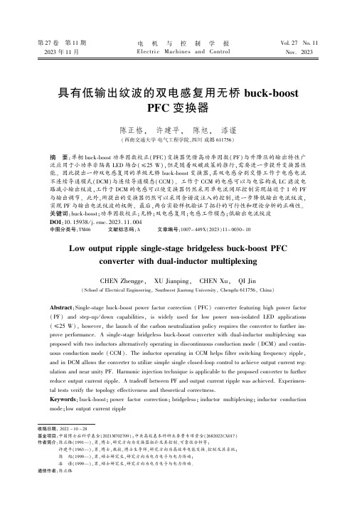
第27卷㊀第11期2023年11月㊀电㊀机㊀与㊀控㊀制㊀学㊀报Electri c ㊀Machines ㊀and ㊀Control㊀Vol.27No.11Nov.2023㊀㊀㊀㊀㊀㊀具有低输出纹波的双电感复用无桥buck-boostPFC 变换器陈正格,㊀许建平,㊀陈旭,㊀漆谨(西南交通大学电气工程学院,四川成都611756)摘㊀要:单相buck-boost 功率因数校正(PFC )变换器凭借高功率因数(PF )与升降压的输出特性广泛应用于小功率非隔离LED 场合(ɤ25W ),但是随着双碳政策的推行,需要进一步提升变换器性能㊂因此提出一种双电感复用的单级无桥buck-boost 变换器,其双电感分别交替工作于电感电流不连续导通模式(DCM )与连续导通模态(CCM )㊂工作于CCM 的电感可以与电容构成LC 滤波电路减小输出纹波,工作于DCM 的电感可以使变换器仍然采用单电流闭环控制实现接近于1的PF 与输出调节㊂此外,所提出的变换器仍然可以采用含谐波注入的控制,进一步降低输出电流纹波,实现PF 与输出电流纹波的权衡㊂最后,两台实验样机验证了拓扑的可行性和理论分析的正确性㊂关键词:buck-boost ;功率因数校正;无桥;双电感复用;电感工作模态;低输出电流纹波DOI :10.15938/j.emc.2023.11.004中图分类号:TM46文献标志码:A文章编号:1007-449X(2023)11-0030-10㊀㊀㊀㊀㊀㊀㊀㊀㊀㊀㊀㊀㊀㊀㊀㊀㊀㊀㊀㊀㊀㊀㊀㊀㊀㊀㊀㊀㊀㊀㊀㊀㊀㊀㊀㊀㊀㊀㊀㊀㊀㊀㊀㊀㊀㊀㊀㊀㊀㊀㊀㊀㊀㊀㊀㊀㊀㊀㊀㊀㊀㊀㊀㊀㊀㊀㊀㊀㊀㊀㊀㊀㊀㊀㊀㊀㊀㊀㊀㊀㊀㊀㊀㊀㊀㊀㊀㊀㊀㊀㊀㊀㊀㊀㊀㊀㊀㊀㊀㊀㊀㊀㊀㊀㊀㊀㊀㊀㊀㊀㊀㊀收稿日期:2022-10-28基金项目:中国博士后科学基金(2021M702709);中央高校基本科研业务费专项资金(2682022CX017)作者简介:陈正格(1991 ),男,博士,研究方向为变换器拓扑及其控制㊁可靠性分析等;许建平(1963 ),男,博士,教授,博士生导师,研究方向为高效率电能变换㊁控制及其系统;陈㊀旭(1999 ),男,硕士研究生,研究方向为电力电子与电力传动;漆㊀谨(1999 ),男,硕士研究生,研究方向为电力电子与电力传动㊂通信作者:陈正格Low output ripple single-stage bridgeless buck-boost PFCconverter with dual-inductor multiplexingCHEN Zhengge,㊀XU Jianping,㊀CHEN Xu,㊀QI Jin(School of Electrical Engineering,Southwest Jiaotong University,Chengdu 611756,China)Abstract :Single-stage buck-boost power factor correction (PFC)converter featuring high power factor (PF)and step-up /down capabilities,is widely used for low power non-isolated LED applications (ɤ25W),however,the launch of the carbon neutralization policy requires the converter to further im-prove performance.A single-stage bridgeless buck-boost converter with dual-inductor multiplexing was proposed with two inductors alternatively operating in discontinuous conduction mode (DCM)and contin-uous conduction mode (CCM).The inductor operating in CCM helps filter switching frequency ripple,and in DCM allows the converter to utilize simple single closed-loop control to achieve output current reg-ulation and near unity PF.Harmonic injection technique is applicable to the proposed converter to further reduce output current ripple.A tradeoff between PF and output current ripple was achieved.Experimen-tal tests verify the topology effectiveness and theoretical correctness.Keywords :buck-boost;power factor correction;bridgeless;inductor multiplexing;inductor conductionmode;low output current ripple0㊀引㊀言在全球范围内,照明系统消耗了近20%的电力,预计未来20年照明能源需求将进一步增加[1]㊂近十年来,传统光源正被寿命更长㊁发光效率更高的发光二极管(light emitting diode,LED)取代[1-2]㊂目前,LED照明被广泛应用于城市亮化工程㊁无人机表演㊁路灯照明㊁大型场馆照明㊁电动汽车㊁农业等多种场合[3]㊂随着LED的大范围使用,Energy star 等产品性能标识对LED的要求也变得苛刻㊂如2009年生效的标准中,仅要求功率ȡ25W的民用LED照明功率因数(power factor,PF)ȡ0.7,商用LED照明PFȡ0.9;而2011年生效的标准已对功率ȡ5W的LED照明均做出上述要求[4]㊂因此,研究高性能的LED驱动具有超前意义㊂目前,LED驱动主要性能指标包括成本㊁使用寿命㊁效率㊁光谱调节能力㊁光照范围等[4-5]㊂由于应用场合的差异,LED驱动电路的性能侧重点有所不同㊂比如,在街边路灯照明中,由于数量众多的路灯整体能耗大㊁维护成本高,LED装置的使用寿命㊁光照范围与发光效能较为重要[6-7];而在农业应用中,由于植物在不同生长阶段对不同特定波长光源有不同的反应,因此LED装置应具备精细可控的光谱调节能力㊁低启动电流与高效率等特性[8]㊂因此,为应对特定场景的不同要求,相关学者提出不同的功率因数校正变换(power factor correc-tion,PFC)电路驱动LED㊂为延长AC-DC驱动电路的使用寿命,学者们提出多种输出电流纹波抑制㊁消除电路,避免在输出侧使用寿命有限的电解电容[9-12]㊂在液晶显示器中,为实现LED高演色性(color rendering index,CRI),避免传统白光LED色移现象[13],学者们采用多路并联RGB-LED[14]㊁可快速调节母线电压的辅助电路[15]㊁母线电容可控投切[16]等方式;其次,为实现多路输出LED串的均流,简单㊁高效㊁低成本的多种无源均流电路被学者提出与分析[17-19]㊂另外,为降低电价增长带来的变换器运行成本,同时响应低碳的政策号召,各类无桥AC-DC变换器被提出[20-29]㊂这类拓扑不再使用二极管整流桥,而是通过减少电流通路中半导体器件数量实现更低的导通损耗[20]㊂近十年来,基于boost㊁Cuk㊁buck-boost 等广泛应用于AC-DC LED驱动的经典电路拓扑,学者们提出更高效的无桥AC-DC LED驱动变换器[24-27]㊂文献[24]提出基于双并联Cuk变换单元所得的无桥Cuk电路并分析其工作特性㊂文献[25]提出谐振无桥boost LED驱动电路,通过谐振电容均流网络实现多路均流㊂文献[26]基于传统boost PFC与半桥LLC谐振电路的两级架构,提出一种通过器件融合的准单级无桥电路,其具有更少的开关器件㊂文献[27]基于双buck-boost变换单元给出一种低开关管应力的单级无桥buck-boost PFC拓扑,但该类无桥拓扑的双变换单元仅交替工作于半个工频周期,器件利用率不高㊂针对文献[27]的缺点,本文提出一种通过双电感复用实现低输出电流纹波的无桥buck-boost PFC 变换器㊂所提出的变换器具有以下特性:1)其中一个电感与输入侧连接,工作于电流断续导电模式(discontinuous conduction mode,DCM),变换器可采用单闭环控制实现高PF与输出调节;2)另一电感与输出侧连接,工作于电流连续导电模式(continu-ous conduction mode,CCM),滤除更多高次输出谐波,实现低输出纹波;3)类似传统buck-boost PFC变换器,该改进型拓扑仍然可以使用含谐波注入的控制进一步降低输出电流纹波㊂本文分析变换器工作原理,推导PF值㊁输出纹波i o,rip表达式,给出谐波注入的控制方法㊂最后,通过实验验证拓扑的可行性与理论分析的正确性㊂1㊀无桥buck-boost PFC变换器1.1㊀提出的拓扑介绍由于buck-boost PFC变换器的功率通常仅为数十瓦,一般采用简单的单电流闭环控制㊂图1给出了传统buck-boost PFC变换器主电路图,包括二极管整流桥㊁开关管S㊁二极管D㊁输出电容C o㊁电感L㊁电磁干扰(electromagnetic interference,EMI)滤波电容C f㊁电感L f㊂图1㊀传统buck-boost PFC变换器及其控制Fig.1㊀Conventional buck-boost PFC converter and its control schematic13第11期陈正格等:具有低输出纹波的双电感复用无桥buck-boost PFC变换器图2(a)㊁图2(b)分别给出了单电流闭环控制和含谐波注入的单电流闭环控制无桥buck-boostPFC 变换器原理图㊂在无桥buck-boost PFC 拓扑中,包括整流二极管D R1和D R2㊁开关管S 1和S 2㊁输出二极管D 1和D 2㊁电感器L 1和L 2㊁输出电解电容C 1和C 2以及双向中间电容C 3㊂其中,S 1㊁S 2的驱动信号V gs1㊁V gs2可以完全相同,实现控制简化㊂在无桥buck-boost PFC 拓扑[22]中,由S 1㊁D 1㊁L 1和S 2㊁D 2㊁L 2组成的双buck-boost 变换单元分别仅工作在正㊁负半个工频周期,变换器整体器件利用率不高㊂本文仅增加中间电容C 3(如图2所示),可以使得双电感在半个工频周期内,分别工作于DCM 与CCM,且未增加控制复杂性㊂图2㊀提出的无桥buck-boost PFC 变换器及两种控制方法Fig.2㊀Proposed bridgeless buck-boost PFC converterand its two control schematics1.2㊀工作模态为简化分析,作如下假设:1)所有器件为理想器件;2)工频周期远大于开关周期T S ,输入电压v in 在一个开关周期内可以认为是常数㊂由于无桥buck-boost PFC 变换器在正㊁负半个工频周期的运行模式相似,本文仅给出正半工频周期工作模态图,如图3所示㊂图4给出了半个工频周期与开关周期所对应的主要器件波形图㊂由图3与图4可知,所提出的buck-boost PFC 变换器由于交流输入过零换流而存在两种工作阶段:1)当交流输入处于过零换流阶段时,变换器中间电容电压v C 3也需要完成换向;此时,变换器工作模态为A1~A3,v C 3电压不断增大,且只有一个电感处于DCM;2)当中间电容电压v C 3足够大(即存储能量足够大)时,C 3可以支撑闲置电感开始运行于CCM;此时,变换器开始运行于主要工作模态,其工作模态为B1~B4,且两个电感分别工作于CCM 与DCM㊂下边对第一㊁第二工作阶段分别进行介绍㊂首先介绍A1~A3工作模态对应的第一工作阶段㊂工作模态A1[t A0~t A1]:如图3(a)所示,当S 1导通时,v in 对L 1充电,i L 1线性增大㊂同时,C 1与C 2为负载供能㊂此阶段,i L 1增大,V C 1㊁V C 2减小㊂工作模态A2[t A1~t A2]:如图3(b)所示,当S 1关断时,i L 1通过D 1向C 1㊁C 3与负载供能,C 2继续为负载供能㊂此阶段,i L 1㊁V C 2减小,V C 1㊁v C 3增大㊂工作模态A3[t A2~t A3]:如图3(c)所示,S 1保持关断,当i L 1下降至0时,此工作模态开始㊂C 1与C 2为负载供能㊂此阶段V C 1㊁V C 2减小,v C 3不变㊂在工作模态A1~A3所示的第一工作阶段中,v C 3不断增大,V C 2不断减小,直到v C 3>V C 2时,电感L 2的两端电压v L 2不为0,变换器进入第二工作阶段,其工作模态为B1~B4㊂工作模态B1[t B0~t B1]:如图3(d)所示,当S 1导通时,v in 对L 1充电,i L 1线性增大㊂同时,L 2㊁C 3㊁C 1存储的能量向输出电容C 2与负载传递㊂此阶段,i L 2㊁v C 3㊁V C 1减小,i L 1增大㊂工作模态B2[t B1~t B2]:如图3(e)所示,当S 1关断时,i L 1通过D 1向C 1㊁负载供能㊂同时,i L 1较大的电流会导致中间电容C 3的电流方向瞬间突变㊂此时,i L 1㊁i L 2非线性减小,v C 3非线性增大㊂当v C 3增大并超过V C 2,则由于v L 2=V C 2-v C 3<0而导致i L 1开始向L 2充电,即i L 2达到谷值i L 2,va 并开始增大㊂此阶段,i L 1减小,V C 1㊁v C 3增大㊂工作模态B3[t B2~t B3]:如图3(f)所示,S 1保持关断,当i L 1下降到与i L 2相等时(即i C 3=0,因为i L 1=i L 2+i C 3),该工作模态开始㊂该阶段,v C 3不断减小,且i C 3(i L 1<i L 2)反向电流不断增大,即中间电容C 3向C 2㊁L 2传能㊂此阶段,i L 1㊁V C 1非线性下降,其中i L 1保持下降至0,i L 2增大,V C 1㊁v C 3减小㊂23电㊀机㊀与㊀控㊀制㊀学㊀报㊀㊀㊀㊀㊀㊀㊀㊀㊀㊀㊀㊀㊀第27卷㊀图3㊀提出的变换器交流换流时工作模态与主模态Fig.3㊀AC input transition operation modes and main operation modes of proposedconverter图4㊀不同工作模态的关键器件波形图Fig.4㊀Theoretical waveforms of key components in different operation modes㊀㊀工作模态B4[t B3~t B4]:如图3(g)所示,S 1保持关断,当i L 1下降到0时,该工作模态开始㊂该阶段,i L 1保持为0,L 2㊁C 3㊁C 1存储的能量向输出电容C 2与负载传递㊂此阶段,v C 3㊁V C 1非线性减小,i L 2非线性增大㊂当v C 3不断下降并小于V C 2时,则由于v L 2=V C 2-v C 3>0而导致i L 1达到峰值I L 2,pk ,i L 1开始下降㊂此阶段,V C 1㊁v C 3减小㊂2㊀变换器PF 与输出纹波性能分析2.1㊀PF 分析令输入电压峰值为V M ,角频率为ω,则v in 为v in (t )=V M sin(ωt )㊂(1)开关管的平均电流i S1,ave 可以看作输入电流i in ,表达式为i in (t )=i S1,ave (t )=V M |sin(ωt )|d 2L2L 1f S㊂(2)式中:d L 为电感的充电时占空比(即开关管的导通占空比);f S 为开关频率;sin(ωt )的绝对值表示变换器工作于正半工作周期㊂根据式(1)㊁式(2)可以推导瞬时输入功率p in与平均输入功率P in 为:p in (t )=i in (t )v in (t )=(d L V M )22L 1f S sin 2(ωt );(3)P in=1T L /2ʏT L /2i in (t )v in (t )d t =(d L V M )24L 1f S㊂(4)33第11期陈正格等:具有低输出纹波的双电感复用无桥buck-boost PFC 变换器根据式(4)可以推导出导通占空比d L 的表达式为d L =2L 1f S P in /V M ㊂(5)由式(5)可知,在理想条件下,由于L 1㊁f S ㊁P in 与V M 是固定值,占空比d L 也相对固定㊂另一方面,忽略由于使用EMI 滤波器导致的输入电压与输入电流的相位偏移,可以推导变换器的理论PF 为PF =P inV rms I rms =(d L V M )2/42L 1f SV M2ʏT L /2[i in (t )]2d t /T L=1㊂(6)式(6)表明,所提出的变换器在理想情况可以与传统buck-boost PFC 变换器一样,实现高PF㊂这是由于所提出的变换器与输入侧连接时,其工作模态与传统变换器基本相同㊂2.2㊀输出纹波与参数分析将输出星接电容等效为三角接电容,可以得到图5(a)所示的变换器工作等效电路图㊂其中C 1㊁C 2㊁C 3与等效电容C 1E ㊁C 2E ㊁C 3E 的关系为:C 1E =C 2E =C 2C 3C 1+C 2+C 3;C 3E=C 1C 2C 1+C 2+C 3㊂üþýïïïï(7)进一步地,可以将工作等效电路简化为如图5(b)所示的输出等效电路㊂在图5(b)中,相对于传统buck-boost PFC 变换器,所提出变换器的输出等效电路增加了LC 滤波㊁等效电容C 1E ㊂因此,理论上,具备实现更小的输出电流纹波的条件㊂根据式(3)㊁式(4)可知,p in =2P in sin(ωt )㊂输出二极管D 1的平均电流i D1,avg 可以表示为i D1,avg (t )=p in (t )V o =2|sin ωt |2P inV o=I o -I o cos(2ωt )㊂(8)式中I o 为输出电流平均值㊂为简化分析,仅对二倍工频谐波进行输出纹波分析,建立如图5(b)所示的输出等效电路㊂图5(b)中的等效阻抗Z eq 可以采用诺顿定理推导得到,即Z eq=(R ESR -j /2ωC 3E )(Z LC -j /2ωC 1E )R ESR -j /2ωC 3E -j /2ωC 1E +Z LC㊂(9)式中Z LC =L 1C 1E (j2ωL 1-j /2ωC 1E )㊂在图5(b)中,仅考虑输出二倍工频纹波电流(即-I o cos(2ωt ))在负载R L ㊁等效阻抗Z eq 的分流情况㊂则等效电流源I ㊃eq 为I㊃eq=I ㊃o(j /2ωC 1E )Z LC -j /2ωC 1E =I ㊃o -2j ωZ LC C 1E -1㊂(10)由式(9)㊁式(10)可以得到输出二倍工频纹波在负载侧的表达式为I ㊃RL=-Z eq I ㊃o(Z eq+R L )(2j ωZ LC C 2E +1)㊂(11)最后,变换器的输出电流纹波i o,rip 为i o,rip (t )=|I㊃RL|cos{2ωt +arctan[imag(I ㊃RL )real(I ㊃RL )]}㊂(12)图5㊀提出变换器的等效电路Fig.5㊀Equivalent circuit of the proposed converter为反映输出纹波随电容㊁电感参数的变化情况,选取典型值I o =0.5A,ω=100πrad /s,R L =50Ω,C 3=0.47μF,R ESR =20mΩ㊂根据式(12)可以得到,输出纹波电流i o,rip 峰-峰值随输出电容C 1㊁C 2与电感L 1㊁L 2的变化曲面,如图6所示㊂由图可知,所提出的变换器输出纹波电流i o,rip 主要受到输出电容C 1㊁C 2影响,即电容值越大则输出纹波越小,符合输出电容越大对二倍工频纹波滤波效果越强的规律㊂另外,电感L 1㊁L 2对i o,rip 的影响比较小,表现为电感值越大则输出纹波越小㊂43电㊀机㊀与㊀控㊀制㊀学㊀报㊀㊀㊀㊀㊀㊀㊀㊀㊀㊀㊀㊀㊀第27卷㊀图6㊀输出电流纹波随电感、电容的变化曲面Fig.6㊀Output current ripple with output capacitorsand inductors as variables2.3㊀谐波注入控制通过在控制部分引入输入谐波分量可以实现输入功率因数与输出纹波的权衡控制[9-10]㊂这种控制本质是降低PF 值至一定值(通常ȡ0.9),以实现更低的输出电流纹波㊂在实际应用中,较高的PF 值不会带来经济效益,而较低的输出纹波可以让厂家选用更小容值的低成本电容达到同样的输出纹波要求,经济效益更高㊂本文提出的无桥buck-boost PFC 变换器同样可以采用这种PF 与输出纹波的权衡控制,图2(b)给出了控制实现框图㊂这种谐波注入的控制策略,在输入功率P in 较小时,采用较大占空比;在P in 较大时,采用较小占空比,可以实现输入功率平滑传输至输出侧,减小输出纹波㊂具体占空比d L ,H 为d L ,H =ad L (1-k |sin ωt |)=2aL 1f S P in (1-k |sin ωt |)/V M ㊂(13)式中a 与k 都是常数㊂为确定a 与k 值,将式(13)中的d L ,H 代替式(4)中的d L ,可以得到谐波注入控制下的P in,H 为P in,H=2P in a 2πʏπ|sin ωt |2[1-k |sin ωt |]2d(ωt )=2P in a 2π(3πk 28-8k 3+π2)㊂(14)由于P in =P in,H ,因此,由式(14)可得a =π/(34πk 2-163k +π)㊂(15)当占空比由d L ,H 确定时,谐波注入控制下的PF 为PF =2(38k 2π-83k +π2)πʏπ{sin(ωt )[1-k |sin(ωt )|]2}2d(ωt )=2(38k 2π-83k +π2)π(516πk 4-6415k 3+94πk 2-163k +π2)㊂(16)根据式(16),图7给出了以k 为变量的PF 曲线㊂为保证PF ȡ0.9,k 可以取0.607㊂由k =0.607,可以通过式(15)确定a =2.017,则式(13)中的d L ,H 为d L ,H =4.034L 1f S P in [1-0.607|sin(ωt )|]/V M ㊂(17)根据式(3)可以得到单闭环控制的无桥buck-boost PFC 变换器瞬时输出电流为i o (t )=p in /V o =P in[1-cos(2ωt )]/V o ㊂(18)同理,根据式(18)可以得到含谐波注入的单闭环控制时的变换器瞬时输出电流为i o,H (t )=㊀4.068P inV o[1-0.607sin(ωt )]2[1-cos(2ωt )]㊂(19)图7㊀PF 随k 值的变化曲线Fig.7㊀PF curve with constant k as variable将式(18)㊁式(19)中的输出电流除以输出电流I o (I o =P in /V o )进行标幺化,可以得到i o(Norm)(t )=1-cos(2ωt );(20)i o,H(Norm)(t )=4.068[1-0.607sin(ωt )]2ˑ[1-cos(2ωt )]㊂(21)根据式(20)㊁式(21),图8给出了两种控制方法所对应的输出电流标幺值㊂可以看到,采用含谐波注入的单电流闭环控制方法可以减小输出电流的53第11期陈正格等:具有低输出纹波的双电感复用无桥buck-boost PFC 变换器波动,降低输出电流纹波㊂但是,该方法的代价就是如图7所示的PF 值仅大于等于0.9㊂图8㊀两种控制方法输出电流标幺值Fig.8㊀Normalized output current under two controlmethods3㊀实验验证由于单级buck-boost PFC 变换器通常应用于功率ɤ25W 的非隔离LED 应用场合[4]㊂因此,为验证所提出的变换器可行性,分别构建了13W 的传统buck-boost PFC 变换器(Conv.)和所提出的buck-boost PFC 变换器(Prop.)实验样机㊂其中,传统buck-boost PFC 变换器通过图1(a)所示的控制原理图实现㊂为保证控制环路参数的一致性以及实验简便性,样机均采用DSP TMS320F28335实现闭环控制㊂表1给出了关键电路参数,C 1㊁C 2串联,所以C 1=C 2=2C ,V C 1=V C 2=1/2V C ㊂图9给出了所提出的变换器实验样机,传统buck-boost PFC 变换器实验样机基于同一PCB 改造得到㊂开关管S㊁S 1㊁S 2为IPW65R125C7,整流和输出二极管为IDH06G65C5,电感L ㊁L 1㊁L 2磁芯为美磁Kool Mμ77206A7,C ㊁C 1㊁C 2均为电解电容,C 3为MKT1822系列的薄膜电容㊂注意,由于输出电容C 1和C 2是串联的(见图2),因此,C 1和C 2的电容值应为C (见图1)的两倍,但是,C 1和C 2的耐压值仅为C 的1/2㊂表1㊀电路参数Table 1㊀Circuit parameters㊀参数传统变换器所提出变换器f S /kHz 5050V in /f L 110Vac /50Hz 110Vac /50Hz I o /P o 0.5A /13W0.5A /13WL /μH140140C ∗150μF /35V300μF /16VC 3 0.47μF /63V图9㊀所提出的电感复用无桥buck-boost PFC 变换器样机Fig.9㊀Prototype of the proposed bridgeless buck-boostPFC converter with multiplexing inductors㊀㊀在110Vac 输入电压时,分别对传统buck-boost PFC 变换器与所提出的电感复用无桥buck-boost PFC 变换器实验样机进行测试㊂表2给出了具体的实验结果对比㊂表2㊀Buck-boost PFC 变换器实验结果Table 2㊀Experimental results of compared converter㊀参数传统变换器(单闭环控制)提出的变换器(单闭环控制)提出的变换器(含谐波单闭环控制)PF0.9980.9980.908THD i /% 2.9 3.345.6i o,rip /mA220190140Eff./%78.181.380.1图10给出了传统buck-boost PFC 变换器的实验波形㊂由图10(a)㊁图10(b)可知,传统变换器的电感电流i L 在每个交流工频周期中均运行于DCM,开关管漏源两端电压V ds 包络线跟随整流后输入电压V d ㊂结合图10(c)可知,这种传统变换器可以采用简单的单电流环实现稳定运行与输入电流高正弦性㊂图11给出了所提出的电感复用buck-boost PFC 变换器在单电流环控制下的实验波形㊂由图11(a)㊁图11(b)可知,在半个工频周期内,电感电流i L 1㊁i L 2分别交替工作于DCM 与CCM,验证了变换器电感的双工作模态;且中间电容电压v C 3经过短暂的换流后,与工作于CCM 的电感电流形成如图4所示的能量交互,即中间电容C 3与CCM 电感组成滤波网络实现变换器低输出纹波特性㊂另外,结合63电㊀机㊀与㊀控㊀制㊀学㊀报㊀㊀㊀㊀㊀㊀㊀㊀㊀㊀㊀㊀㊀第27卷㊀图11(c)可知,所提出的变换器在单电流环控制下的输出电流纹波为190mA,与图6所示的理论计算值(206mA)接近(注:由于器件参数偏差与测量误差等因素,理论计算值与实际测量值存在一定的偏差)㊂图10㊀传统buck-boost PFC 变换器在单电流环控制时的实验波形Fig.10㊀Experimental waveforms of conventional buck-boost PFC converter图12给出了所提出的变换器在含谐波注入时的单电流环控制下的实验波形㊂由图12(a )㊁图12(b)可知,变换器电感仍然交替地工作于DCM 与CCM,未受到谐波注入的影响㊂结合图12(c)可知,在这种谐波注入控制方式下,变换器输入电流i in 有所畸变,但是变换器PF 值维持在0.908,与图7的理论计算值(PFȡ0.9)接近,验证了参数设计的准确性㊂图11㊀提出的无桥buck-boost PFC 变换器在单电流环控制时的实验波形Fig.11㊀Experimental waveforms of proposed bridge-less buck-boost PFC converter在输出电流纹波i o,rip 方面,对比图10(c)和图11(c),所提出的变换器输出电流纹波(190mA)比传统变换器(220mA)更小㊂这是因为所提出变换器的一个电感与中间电容C 3构成了LC 滤波,可以进一步减小输出纹波㊂另外,对比图11(c)和图12(c),输出电流纹波i o,rip 由190mA 降低到了140mA,降低了35.7%,验证了所提出变换器在含谐波注入控制时,可以实现更低的输出电流纹波㊂在PF㊁THD i 方面,传统变换器的PF 和THD i 分别为0.998和2.9%㊂相应地,所提出的变换器在同样的单电流闭环控制时,PF 和THD i 分别为0.99873第11期陈正格等:具有低输出纹波的双电感复用无桥buck-boost PFC 变换器和3.3%㊂两种变换器的测量数据相近,表明当所提出的变换器与传统变换器使用同样的控制策略时,他们具有几乎相同的PF 和THD i 性能㊂此外,如2.3节所述,当所提出的变换器使用含谐波注入的控制时,通过设置a ㊁k ,可以保证变换器的PF 值高于0.9(实验中为0.908),但是其输出电流纹波仅为140mA,验证了参数设计与理论分析的正确性㊂图12㊀提出的无桥buck-boost PFC 变换器在含有谐波注入控制时的实验波形Fig.12㊀Experimental waveforms of proposed bridge-less buck-boost PFC converter with the har-monic injection control在效率方面,当所提出的变换器采用无谐波注入控制时,变换器的测量效率为81.3%,当采用谐波注入控制时,该变换器的测量效率为80.1%㊂这是因为在含谐波注入的控制时,更多的输入电流谐波会流入变换器,降低了变换器效率㊂另一方面,传统变换器的测量效率仅为78.1%㊂即所提出的无桥buck-boost PFC 变换器在含谐波注入控制时㊁不含谐波注入控制时的效率都略高于传统变换器㊂4㊀结㊀论本文提出一种双电感复用无桥buck-boost PFC 变换器,提高了双变换单元在无桥拓扑中的器件利用率㊂在半个工频周期内,双电感分别交替工作于DCM㊁CCM,且不需要复杂的控制㊁额外的辅助电路㊂工作于DCM 的电感,使变换器可以采用单闭环控制实现高PF 与输出电流调节;工作于CCM 的电感,与中间电容构成额外滤波电路,减小变换器输出纹波㊂此外,该变换器仍然可以采用含谐波注入的控制方法,通过主动降低PF 至0.908,可降低35.7%的输出电流纹波㊂实验样机验证了理论分析的正确性㊂参考文献:[1]㊀WANG Yijie,ALONSO M,RUAN Xinbo.A review of LED driversand related technologies[J].IEEE Transaction on Industrial Elec-tronics,2017,64(7):5754.[2]㊀沈霞,王洪诚,许瑾.基于SEPIC 变换器的高功率因数LED 照明电源设计[J].电机与控制学报,2010,14(1):41.SHEN Xia,WANG Hongcheng,XU Jin.Design of LED lighting power supply with high power factor based on SEPIC converter [J].Electric Machines and Control,2010,14(1):41.[3]㊀景妍妍,曲小慧,韩洪豆,等.基于可调增益恒流源补偿网络的磁场耦合无线电能传输LED 驱动电路[J].中国电机工程学报,2016,31(S1):1.JING Yanyan,QU Xiaohui,HAN Hongdou,et al.The magnetic coupled wireless power transfer driver based on adjustable gain constant-current compensation network [J ].Proceeding of the CSEE,2016,31(S1):1.[4]㊀罗全明,高聪哲,周雒维.一种ZVT 无整流桥Boost 功率因数校正[J].电机与控制学报,2010,14(10):44.LUO Quanming,GAO Congzhe,ZHOU Luowei.Zero-voltage-transition bridgeless Boost PFC[J].Electric Machines and Con-trol,2010,14(10):44.[5]㊀乔之勇,施怡乐,张良,等.无电解电容LED 驱动电源纹波补偿控制策略综述[J].电源学报,2022,20(3):115.QIAO Zhiyong,SHI Yile,ZHANG Liang,et al.Review of ripple compensation control strategies for electrolytic capacitor-less LED driver[J].Journal of Power Supply,2022,20(3):115.[6]㊀CHENG C,CHANG C,CHUNG T,et al.Design and implementa-tion of a single-stage driver for supplying an LED street-lighting module with power factor corrections [J].IEEE Transactions on Power Electronics,2015,30(2):956.83电㊀机㊀与㊀控㊀制㊀学㊀报㊀㊀㊀㊀㊀㊀㊀㊀㊀㊀㊀㊀㊀第27卷㊀[7]㊀GOBBATO C,KOHLER S,DE-SOUZA I,et al.Integrated topologyof DC-DC converter for LED street lighting system based on modu-lar drivers[J].IEEE Transactions on Industry Applications,2018, 54(4):3881.[8]㊀MA Yuanchun,XU An,CHENG M.Effects of light emitting diodelights on plant growth,development and traits a meta-analysis[J].Horticultural Plant Journal,2021,7(6):552.[9]㊀WU H,WONG S,TSE C,et al.Single-phase LED drivers with min-imal power processing,constant output current,input power factor correction,and without electrolytic capacitor[J].IEEE Transac-tions on Power Electronics,2018,33(7):6159. [10]㊀WANG Haoran,WANG Huai.A two-terminal active capacitor[J].IEEE Transactions on Power Electronics,2017,32(8):5893.[11]㊀GU Linlin,RUAN Xinbo,XU Ming,et al.Means of eliminating e-lectrolytic capacitor in AC/DC power supplies for LED lightings[J].IEEE Transaction on Power Electronics,2009,24(5):1399.[12]㊀WANG Beibei,RUAN Xinbo,YAO Kai,et al.A method of reduc-ing the peak-to-average ratio of LED current for electrolytic ca-pacitor-less AC-DC drivers[J].IEEE Transactions on Power E-lectronics,2010,25(3):592.[13]㊀LO Y,WU K,PAI K,et al.Design and implementation of RGBLED drivers for LCD backlight modules[J].IEEE Transactionson Industrial Electronics,2009,56(12):4862. [14]㊀JHA A,SINGH B.A PFC modified landsman converter-basedPWM-dimmable RGB HB-LED driver for large area projection ap-plications[J].IEEE Transactions on Industry Applications,2017,53(2):1552.[15]㊀LIU Pangjung,PENG Kailin.Adaptive driving bus voltage and en-ergy recycling control schemes for low-power AC-DC RGB-LEDdrivers[J].IEEE Transactions on Industrial Electronics,2017,64(10):7741.[16]㊀LIU Pangjung,HONG Zhiyuan,HUNG Chuncheng.A single-stagelow-power AC-DC RGB-LED driver with switching capacitor con-trol scheme[J].IEEE Transactions on Industrial Electronics,2021,68(4):3103.[17]㊀LIU Xueshan,WAN Yuyang,DONG Zheng,et al.Buck-boost-buck-type single-switch multistring resonant LED driver with highpower factor[J].IEEE Transactions on Power Electronics,2020,35(5):5132.[18]㊀何青青,罗全明,曹驰,等.一种模块化开环多路谐振恒流LED驱动电源[J].中国电机工程学报,2019,39(22):6688.HE Qingqing,LUO Quanming,CAO Chi,et al.A modular open-loop multi-channel resonant constant-current LED driver[J].Pro-ceeding of the CSEE,2019,39(22):6688.[19]㊀GUO Y,LI S,LEE A,et al.Single-stage AC/DC single-inductormultiple-output LED drivers[J].IEEE Transactions on Power E-lectronics,2016,31(8):5837.[20]㊀HUBER L,JANG Y,JOVANOVIC M.Performance evaluation ofbridgeless PFC boost rectifiers[J].IEEE Transactions on PowerElectronics,2008,23(3):1381.[21]㊀胡玮,康勇,王学华,等.一种改进型双升压功率因数校正电路[J].电机与控制学报,2013,17(3):40.HU Wei,KANG Yong,WANG Xuehua,et al.Improved dualboost power factor correction converter[J].Electric Machines andControl,2013,17(3):40.[22]㊀吴红飞,张炎锋,杨帆.宽输出电压范围集成Buck型无桥PFC变换器[J].中国电机工程学报,2018,38(22):6655.WU Hongfei,ZHANG Yanfeng,YANG Fan.Bridgeless power fac-tor correction converter with integrated buck converter for wideoutput voltage range applications[J].Proceeding of the CSEE,2018,38(22):6655.[23]㊀曹太强,黄俊,王军,等.基于磁集成的双Boost无桥PFC变换器研究[J].电机与控制学报,2014,18(4):6.CAO Taiqiang,HUANG Jun,WANG Jun,et al.One-cycle con-trolled bridgeless Pseudo-Boost PFC converter[J].Electric Ma-chines and Control,2014,18(4):6.[24]㊀蔡成超,沈艳霞,赵文辉,等.基于Cuk变换器的无桥LED驱动电源[J].电源学报,2019,17(4):57.CAI Chengchao,SHEN Yanxia,ZHAO Wenhui,et al.BridgelessLED driver based on Cuk converter[J].Journal of Power Sup-ply,2019,17(4):57.[25]㊀史旭,刘雪山,周群,等.基于无源均流的谐振式无桥型BoostLED驱动电源[J/OL].电源学报:1-13[2021-11-22].ht-tp:///kcms/detail/12.1420.TM.20211122.1445.004.html.SHI Xu,LIU Xueshan,ZHOU Qun,et al.A resonant bridgelessboost LED driver based on passive current balancing[J/OL].Journal of Power Supply:1-13[2021-11-22].http://kns./kcms/detail/12.1420.TM.20211122.1445.004.ht-ml.[26]㊀MA Hongbo,LAI J S,ZHENG Cong,et al.A high-efficiency qua-si-single-stage bridgeless electrolytic capacitor-free high-powerAC-DC driver for supplying multiple LED strings in parallel[J].IEEE Transactions on Power Electronics,2016,31(8):5825.[27]㊀CHEN Zhengge,DAVARI P,WANG Huai.Single-stage bridgelessbuck-boost PFC converter with DC split for low power LED appli-cations[C]//2018IEEE International Power Electronics and Ap-plication Conference and Exposition(PEAC),November4-7,2018,Shenzhen,China.2018:1-6.[28]㊀王金平,胡凡宇,侯良奎,等.一种单级无桥隔离型PFC变换器[J].中国电机工程学报,2017,37(24):7276.WANG Jinping,HU Fanyu,HOU Liangkui,et al.An isolated PFCconverter with single-stage and bridgeless properties[J].Proceed-ings of the CSEE,2017,37(24):7276.[29]㊀CHEN Zhengge,LIU Bochen,YANG Yongheng,et al.BridgelessPFC topology simplification and design procedure for performancebenchmarking[J].IEEE Transactions on Power Electronics,2021,36(7):6916.(编辑:邱赫男)93第11期陈正格等:具有低输出纹波的双电感复用无桥buck-boost PFC变换器。
On the design of single-inductor multiple-output DC-DC buck converters
On the Design of Single-Inductor Multiple-Output DC-DC Buck ConvertersMassimiliano Belloni, Edoardo Bonizzoni, and Franco MalobertiDepartment of Electronics University of PaviaVia Ferrata, 1 – 27100 Pavia – ITALY[massimiliano.belloni, edoardo.bonizzoni, franco.maloberti]@unipv.itAbstract –Design techniques for single inductor multiple output (SIMO) DC-DC buck converters are presented. The suitable control of a multiple feedback loop enables the sharing of a single inductor with many outputs with a good stability and limited cross regulation. The method has been verified with simulations at the behavioural and transistor level to obtain four independent regulated output voltages ranging from 0 V to 1 V below the power supply voltage. The use of a suitable analog processing of errors allows obtaining a power efficiency as high as 86%.I.I NTRODUCTION The fast market growth of battery-operated portable applications such as digital cameras, personal digital assistants, cellular phones, MP3 players, medical diagnosis systems, etc. demands for more and more efficient power management systems. In this area, DC-DC converters play a critical role in keeping long battery life while still providing stable supply voltage together with the required driving capability [1]. In these devices, an inductor stores magnetic energy and transfers part of it to a load while another part is converted into electrostatic energy stored in a capacitor. The result is high power efficiency, low cost, and small size [2], [3]. Often, in portable applications, the reduction of power is obtained by using multiple supply voltages for different functional blocks [4]. A dynamic regulation of the supply following the performance requests optimizes the use of power. However, since having in the system one inductor per DC-DC converters is expensive and not practical, the strategy is viable only if two or more converters share the same inductor as proposed in recent implementations (single inductor multiple output boost converter [5] and boost or buck converters with double output [6], [7]).Since the regulation of each output requires its loop control, a multiple-output system must foresee a multi-feedback loop with the request of suitable processing of signals. Moreover, it is necessary to use extra power switches that must be properly driven.This paper studies the above mentioned design problems and applies the identified solutions to a study case: a four-output single inductor buck converter able to independently regulate the output voltages in the range 0 V - 1 V below the power supply voltage and able of an overall driving capability of 0.8 A. The switching frequency is 3 MHz and the external inductor is 1 µH. Transistor level simulations show that a power efficiency as high as 86% can be achieved.II.SIMO A RCHITECTUREA DC-DC converter with multiple outputs time-shares the inductor current among different loads. Fig. 1 shows a buck converter with N -outputs. While a normal buck has just a PWM control for the high-side and low-side switches (namely MP and MN ), the N -output buck uses Nadditional power switches (SW i ,i = 1, …, N ) for the time-sharing of the inductor current. The switches can ben -channel (with possible boost), p -channel or complementary devices. The choice depends on a trade-off between complexity and cost (area, power efficiency and so forth).The control subsystem, together with the drivers, provides N control signals. One is used to obtain the buck converter switching, and the others to divide the clock period into N slots.The processor foresees N control loops with as inputs the errors of the N outputs, εi = V set,i – V out,i . The buck converter operates in the continuous mode, but the current, I i , delivered to the C outi output capacitor, is discontinuous, since it goes to zero when the corresponding switch opens, as shown in Fig. 2 for i = 1, …, 4. During the discontinuous period the current of the load is provided by the capacitance C ou,i.Figure 1. Block diagram of the N -output SIMO buck converter.Figure 2. 4-output SIMO inductor (I L ) and output branches currents (I i ). Fig. 2 shows an example of inductor and load switched currents for four outputs. The diagrams of the figure support the definition of the main duty cycle D and thesharing duty cycles. They can be expressed, respectively, asD =Ton ,MP T(1) D i =T on ,SWi T(2)where T on,MP ,T , and T on,SWi are the on-time of the p -channel switch MP , the clock period, and the on-timeof the i -th n -channel output switch SW i , respectively.III.S INGLE -I NDUCTOR D UAL -O UTPUTC ONTROL E QUATIONSIn order to study the control strategy let us consider before a single-inductor dual-output (SIDO) DC-DC buck converter, as shown in Fig. 3. The figure also depicts the load currents in the cases D < D 1 and D > D 1.If the ripple of the output voltages is small, the derivative of the inductance current in the three time-slots identified by the duty cycles D and D 1 (D 1 + D 2 = 1) can be assumed constant. Therefore, in the steady state we have (V dd −V out ,1)D =V out ,1D 1+V out ,2D 2;for D <D 1(3) (V dd −V out ,1)D 1+(V dd −V out ,2)D 2=V out ,2D 2;for D >D 1 (4) that, after rearranging, both become V dd D =V out ,2+(V out ,1−V out ,2)D 1 (5)Assuming that the inductor current ripple is negligible, its average value I L can be used to determine the outputcurrentsFigure 3. 2-output SIMO and output branches currents (I i ) in the twocases D < D 1 and D > D 1.I L D 1=I out ,1=V out ,1R load ,1I L (1−D 1)=I out ,2=V out ,2R load ,2(6)that givesD 1=R load ,2V out ,1R load ,2V out ,1+R load ,1V out ,2(7)Equation (7) together with (5) makes a system to control D and D 1. Unfortunately, the control is difficult to implement using the errors because it involves nonlinearterms and needs the estimation of the load currents.However, from (5) it can be noted that the main dutycycle is proportional to the weighed sum of the output voltages. With D 1 = ½, (5) becomes D =V out ,1+V out ,22V dd (8) that suggests to control the main duty cycle using the sum of the errors ε1= (V set,1 - V out ,1) and ε2= (V set ,2 -V out ,2). Indeed, the optimum control should account for the value of D 1. However, the use of the plain sum of errors,instead of their dynamic weighted sum, is an affordable(and reasonable) approximation. By differentiating equation (7), it is possible to obtain δD 1=α⋅ε1−β⋅ε2 (9)where α and β are coefficients that depend on the outputvoltages and the load resistances. Therefore, the control loop controlling D 1should use the weighted subtraction of errors. An approximated solution is to use the plain subtraction of errors. The two above strategies for the control of D and D 1 are intuitively justified. In fact, positive errors call for more energy to be delivered to theloads and this is obtained by increasing D (see Fig. 4). A positive ε1 or a negative ε2 indicates the need to increasethe fraction of power delivered to load 1 and vice-versa.The control method for two outputs can be extended to multiple outputs. The sum of errors should control themain duty cycle and proper combinations of errorscontrol the sharing duty cycles. More in general, for an N -output DC-DC buck converter, N control variables X 1, …, X N can be defined.Figure 4. Control of D and D 1 as required by errors ε1 and ε2.X 1=a 11ε1+a 12ε2+!+a 1N εN X 2=a 21ε1+a 22ε2+!+a 2N εN !X N =a N 1ε1+a N 2ε2+!+a NN εN(9)The gain of each control loop must tend to null each error combination in (9), thus leading to: a 11ε1+a 12ε2+!+a 1N εN →0a 21ε1+a 22ε2+!+a 2N εN →0!a N 1ε1+a N 2ε2+!+a NN εN →0 (10) Indeed, equation (10) is an homogeneous system of Nequations in the N unknowns εi . To have only onesolution, the determinant of the system characteristicmatrix must bedeta 11a 12!a 1N a 21a 22!a 2N !!!!a N 1a N 2!a NN≠0 (11) For 4 outputs, a simple form of the characteristic matrix and then the errors coefficients in (9) isX 1=ε1+ε2+ε3+ε4X 2=ε1−ε2−ε3−ε4X 3=ε1+ε2−ε3−ε4X 4=ε1+ε2+ε3−ε4(12) In order to ensure stability to the system, it is necessary toassociate the control voltages X i to proper control variables. In our case X 1,X 2,X 3, and X 4 are related to the duties D ,D 1,D 1 + D 2,D 1 + D 2 + D 3, respectively. Fig. 5 shows the conceptual scheme of the 4-output case control system together with the PWM s output pulses. H(s) in the main path is a first-order zero-pole filter that achieve the loop compensation, while A blocks in the sharing paths are just amplifiers. The main path, driven by H(s)X 1, controls the main switches MP and MN , while the other paths, driven by AX 2,AX 3, and AX 4, manage the sharing of the inductor current, thus determining the fourtime-sharing slots.Figure 5. Conceptual scheme of the analog processorand PWMs output pulses.IV.D ESIGN E XAMPLE The above-described methods have been tested on a 4-output design, simulated at the behavioural, transistor level (with a 0.18-µm CMOS technology), redesigned and fabricated on silicon using a 0.5-µm 2-poly, 5-metalsCMOS technology. A short description of that design and the experimental results is given in [8]. The targetspecifications of this design example are to have a totalcurrent up to 0.8 A, a switching frequency of 3 MHz with a single 1-μH inductor and 10-μF capacitors. The simulations at the behavioural level show an excellentmatching with the expected results. Fig. 6 shows theinductor current (top) and its sharing among the four output branches (bottom). The inductor current ripple isin the range from 0.32 to 0.54 A and shows the change ofslope due to the different regulated voltages. Otherperformance are also verified.Figure 6. Simulink™ simulation result of the inductor current. Figure 7. Detail of the main processing path.After the behavioural simulations, which prove the system functionality, transistor level simulations provide additional verifications of the circuit operation. The technology used is a 0.18-µm CMOS technology with high voltage option. The signal processing required by (12) can be realized in the analog or the digital domain. In the latter case, it is necessary to have an on-board A/D converter as it is often done in modern buck converter. For analog implementations, the use of switched-capacitor schemes is a convenient choice because they enable inverting and non-inverting functions. Fig. 7 shows the scheme for the main processing path. It consists of three blocks. The first section combines the errors and provides a gain; the second is the first order zero-pole switched-capacitor filter. C 5 and V bias achieves a DC level shift. The third block is a the flip around doublesample-and-hold necessary to decouple the filter from the PWM , thus limiting the kickback from the switching part and eliminating the glitches produced by the switching from phase 1 to phase 2.The other processing channels do not require filtering and are realized with only two sections. One is to process the errors, providing gain and shifting the DC level; the other is the sample-and-hold.Fig. 8 shows the simulated output voltages V outi regulated at 0.85 V, 1.5 V, 1.2 V, and 1.78 V, respectively. The power supply voltage is equal to 3.3 V. The output currents are I out 1 = 45 mA, I out 2= 350 mA, I out 3= 40 mA,and I out 4=180 mA, thus achieving a total delivered output current of 0.615 A. The simulated maximum output voltage ripple is about 25 mV (V out 3).Figure 8. Simulated output voltages.Fig. 9 shows the results of a cross-regulation test. V out 4 is set to 1.8 V driving 300 mA to its load. V out 1 and V out 2present a step-up variation from 1.2 to 1.7 V and from 0.8 to 1.6 V, respectively. I out 1 and I out 2 rise up from 150 to 212 mA and from 50 to 100 mA, respectively. V out 3 has a step-down variation from 1.4 V to 0.9 V and its current decreases from 70 to 45 mA. The output voltage drop dueto the cross-regulation is less then 24 mV.Figure 9. Cross-regulation simulations.Fig. 10 shows the simulation results of a load-regulation test with a supply voltage of 3.3 V. The four outputvoltages V outi are set to 1.2V, 1 V, 1.6 V, and 1.8 V, respectively. I out1 and I out3 have a step-up variation from 75 mA to 240 mA and from 150 mA to 250 mA, respectively, while I out2 and I out4 present a step-down variation from 200 mA to 100 mA and from 300 mA to125 mA, respectively. The output voltage drops due to the load-regulation is less then 1.5% in all cases.Several simulations have been performed in order to evaluate the system power efficiency performance. The simulated peak of power efficiency is 86%, considering a supply voltage of 3.3 V and an overall output current equal to 400 mA. With other conditions the efficiency islower but within the entire range of specifications thepower efficiency is always higher than 74%. Figure 10. Load-regulation simulated results.V.C ONCLUSIONSIn this paper, the design methodologies for single-inductor multiple-output DC-DC buck converter have been presented. The new control method suitable for any number of outputs is more robust than 2-output counterparts. The approach has been verified for 4 outputs with behavioural simulations and transistor level verifications. With a 0.18-μm CMOS technology, it is possible to achieve a 0.8 A driving capability with a peak of efficiency of 86%. The same design method has been used for a 0.5-μm CMOS technology that experimentally verified the approach functionality, [8].R EFERENCES[1] N. Mohan, T.M. Undeland, and W.P. Robbins, “Power E lectronics -Converters, Applications, and Design – Second Edition”, John Wiley & Sons, INC., Ch. 7.[2] B. Arbetter, R. E rickson, and D. Maksimovic, “DC-DC converter design forbattery-operated systems”, IEEE Power Electronics Specialist Conference 1995, vol. 1, pp. 103 – 109, June 1995.[3] V. Kursun, S.G. Narenda, V.K. De, and E.G. Friedman, “Analysis of buckconverters for on-chip integration with a dual supply voltage microprocessor”, IEEE Trans. on Very Large Scale Integration (VLSI) Systems , vol. 11, pp. 514 – 522, June 2003. [4] J.M. Chang and M. Pedram "E nergy minimization using multiple supplyvoltages", IEEE Trans. on Very Large Scale Integration (VLSI) Systems ,pp.436 – 443, Dec. 1997.[5] H.-P. Le, C.-S. Chae, K.-C. Lee, G.-H. Cho, S.-W. Wang, G.-H. Cho, and S.-I. Kim, “A Single-Inductor Switching DC-DC Converter with 5 Outputs and Ordered Power-Distributive Control”, IEEE International Solid-State Circuits Conf. (ISSCC) Dig. Tech. Papers , pp. 534 – 620, Feb. 2007.[6] D. Ma, W.-H. Ki, and C.-Y. Tsui, “A pseudo-CCM/DCM SIMO switchingconverter with freewheel switching”, IEEE International Solid-State Circuits Conf. (ISSCC) Dig. Tech. Papers , pp. 390 – 476, Feb. 2002.[7] E. Bonizzoni, F. Borghetti, P. Malcovati, F. Maloberti, and B. Niessen, “A200mA 93% Peak E fficiency Single-Inductor Dual-Output DC-DC Buck Converter, IEEE International Solid-State Circuits Conf. (ISSCC) Dig. Tech. Papers , pp. 526 – 619, Feb. 2007. [8] M. Belloni, E . Bonizzoni, E . Kiseliovas, P. Malcovati, F. Maloberti, T.Peltola, and T. Teppo, “A 1.2A Output Current Single-Inductor 4-Outputs DC-DC Buck Converter with Self-Boosted Switch Drivers”, to appear in 2008 IEEE International Solid-State Circuits Conf. (ISSCC) Dig. Tech . Papers .。
固定导通时间I2控制BuckLED驱动器研究
固定导通时间 I2控制 Buck LED驱动器研究摘要:I2控制Buck LED驱动器的稳定性受输出电容等效串联电阻(ESR)的影响较大,当ESR较小时,驱动器将处于不稳定的状态下。
为了消除ESR对I2控制Buck LED驱动器稳定性的影响,提出固定导通时间I2控制Buck LED驱动器。
详细分析了固定导通时间I2控制Buck LED驱动器的工作原理,并与I2控制Buck LED驱动器进行对比分析。
研究结果表明:本文提出的固定导通时间I2控制Buck LED驱动器不受输出电容ESR的影响。
最后,通过时域仿真验证了分析的正确性。
关键词:LED驱动器;固定导通时间控制;稳定性;瞬态响应Research on Constant On-time I2Controlled Buck LED ConstantCurrent DriverZHANG Liuyang(Key Laboratory of Electronic Information of State Ethnic AffairsCommission,College of Electrical Engineering,Southwest Minzu University,Chengdu 610041,Sichuan,China)Abstract: The stability of I2 controlled Buck LED driver is greatly affected by the equivalent series resistance (ESR) of the output capacitor. When the ESR is small, the driver will be in an unstable state. In order to eliminate the influence of ESR on the stability of the I2 controlled Buck LED driver, a constant on-time I2 controlledBuck LED driver is proposed. The working principle of the constant on-time I2 controlled Buck LED driver is analyzed in detail, and comparedwith the I2 controlled Buck LED driver. The research results show that: the constant on-time I2 controlled Buck LED driver is proposed in this paper without being affected by the ESR of the output capacitor. Finally, the correctness of the analysis is verified by time-domain simulation.keywords:LED driver; constant on-time controlled; stability; transient response1.引言LED (Light Emitting Diode)凭借着体积小、节能环保等优点,广泛应用在通用照明、电子设备等领域[1-2]。
UC3842 提供低成本电流模式控制
应用笔记U-100AU-100AAPPLICATION NOTEUC3842/3/4/5 PROVIDES LOW-COSTCURRENT-MODE CONTROLINTRODUCTIONCURRENT-MODE CONTROLThe fundamental challenge of power supply design is to simultaneously realize two conflicting objectives: good electrical performance and low cost. The is an integrated pulse width modulator designed with both these objectives in mind. This provides de-signers an inexpensive controller with which they can ob-tain all the performance advantages of current mode op-eration. In addition, the UC3842 series is optimized for ef-ficient power sequencing of off-line converters, DC to DC regulators and for driving power MOSFETs or transistors.This application note provides a functional description of the UC3842 family and highlights the features of each in-dividual member, the UC3842, UC3843, UC3844 and UC3845 Throughout the text, the UC3842 part number will be referenced, however the generalized circuits and performance characteristics apply to each member of the UC3842 series unless otherwise noted. A review of cur-rent mode control and its benefits is included and meth-ods of avoiding common pitfalls are mentioned. The final section presents designs of power supplies utilizing UC3842 control.Figure 1 shows the two-loop current-mode control system in a typical buck regulator application. A clock signal initi-ates power pulses at a fixed frequency. The termination of each pulse occurs when an analog of the inductor current reaches a threshold established by the error signal. In this way the error signal actually controls peak inductor cur-rent. This contrasts with conventional schemes in which the error signal directly controls pulse width without regard to inductor current.Several performance advantages result from the use of current-mode control. First, an input voltage feed-forward characteristic is achieved; i.e., the control circuit instanta-neously corrects for input voltage variations without using up any of the error amplifier’s dynamic range. Therefore,line regulation is excellent and the error amplifier can be dedicated to correcting for load variations exclusively.For converters in which inductor current is continuous,controlling peak current is nearly equivalent to controlling average current. Therefore, when such converters employ current-mode control, the inductor can be treated as anFigure 1. Two-Loop Current-Mode Control SystemUC3842/3/4/5提供了低成本的电流模式控制引言电源设计的主要难题是需要同时实现两个相互矛盾的目标,即:上佳的电性能和低成本。
开关电源输入输出电容的选择
1.2
Selecting Input Ceramic Capacitors
Load current, duty cycle, and switching frequency are several factors which determine the magnitude of the input ripple voltage. The input ripple voltage amplitude is directly proportional to the output load current. The maximum input ripple amplitude occurs at maximum output load. Also, the amplitude of the voltage ripple varies with the duty cycle of the converter. For a single phase buck regulator, the duty cycle is approximately the ratio of output to input dc voltage. A single phase buck regulator reaches its maximum ripple at 50% duty cycle. Figure 1 shows the ac rms, dc, and total rms input current vs duty cycle for a single phase buck regulator. The solid curve shows the ac rms ripple amplitude. It reaches a maximum at 50% duty cycle. The chart shows how this magnitude falls off on either side of 50%. The straight solid line shows the average value or dc component as a function of duty cycle. The curved dashed line shows the total rms current, both dc and ac, of the rectangular pulse as duty cycle varies.
- 1、下载文档前请自行甄别文档内容的完整性,平台不提供额外的编辑、内容补充、找答案等附加服务。
- 2、"仅部分预览"的文档,不可在线预览部分如存在完整性等问题,可反馈申请退款(可完整预览的文档不适用该条件!)。
- 3、如文档侵犯您的权益,请联系客服反馈,我们会尽快为您处理(人工客服工作时间:9:00-18:30)。
II. CIRCUIT ARCHITECTURE AND CONTROL STRATEGY
Fig. I shows the power stage of the proposed
smo
Yang Yang is the Ph. D student with the Institue of VLSI, Zhejiang University, Hangzhou, China. Email: yangyang@vlsLzj Sun Liang is the master student with the Institue of VLSI, Zhejiang University, Hangzhou, China. Wu Xiaobo is the professor with the Institue ofVLSI, Zhejiang University, Hangzhou , China.
~T l +T2+T l·i·T2~ IL" ! A ! A ! A- !r-. ! A f"'Idc1 o ~idc- ---- - ---Y- - ----- ~- - - - - --- --~-Ie - - j -CCM
Advantage: drive large load with small ripple Disadvantage: cross regulation and hard compensation
DCM
Advantage: no cross regulation and easy compensation Disadvantage: large current ripple when drive large load
Fig. 2 Features of CCM and DCM.
IL~ o: :::: ::: :::: :::: ::I'd c
S.~
S2ቤተ መጻሕፍቲ ባይዱ
3.3V. And the conversion efficiency of 88% at 300mW is achieved. Keywords: sino, PCCM, Buck
---cri-H
I I I I I I I I I I I I I I I
L.. '-T . :
.J -,
: ,
Sp. T1 and T2 are two complementary phases. During T1,
converter controller is presented, which operates in (PCCM) with adjustable de current levels. Freewheel switching control has been introduced to realize large load current with smaller current ripple, while cross regulation can be minimized. Furthermore, the de current level of subconverters can be adjusted according to each load. The controller was designed and fabricated in 1.5
: ,
S~
Fig. 1 Power stage of the timing diagram.
I. INTRODUCTION
It is important to minimize the power supply in
IL~__
smo buck converter and the
portable electronic equipments such as personal digital assistants (PDA), microprocessors, mobile phones, etc. Thus, the power supply with multiple and variable output voltage has got great attentions[I]. However, the conventional solutions usually use multiple inductors in it[2], which is huge in volume, costly and has weak immunity to electro magnetic interference (EMI). In this paper, a single-inductor dual-output buck converter controller is proposed. With a proposed freewheel switching control, the current of inductor maintains above zero as a CCM converter does to handle large current with smaller current ripple, and the cross regulation can be minimized also. Using current sensor and other functional circuits, the inductor de current of subconverters can be adjusted according to different loads, thus the self-adapted control strategy is realized.
PCCM (with a fixed dc level) Advantage: no cross regulation, easy compensation and small ripple when drive large load
~TI +j+T2+j+TI.~T2~
Id
PCCM (with different dc levels) Advantage: no cross regulation, easy compensation, small ripple when drive large load and adapt to different loads Tsadrntar: crn nOf driy variiable iloadsi
A Single-Inductor Dual-Output Buck Converter with Self-Adapted PCCM Method
Yang Yang, Sun Liang, Wu Xiaobo
Abstract self-adapted A single-inductor dual-output (SmO) buck pseudo-continuous-conduction-mode buck converter and the timing diagram of it. The two outputs VOl and V02 share the inductor L and the switch
For dual-output converter with stable outputs, each output should be independently regulated. When load of one subconverter changes, the other output voltage will be affected, this is cross regulation. Due to the inductor current goes zero in each period in discontinuous conduction mode (DCM), the load variation in one output does not affect the other, thus the two outputs can be isolated in DCM, and cross regulation can be minimized. Furthermore, compensation is simple for DCM system because there is only one LHP pole in the gain transfer function of control-to-output. Unfortunately, DCM can only provide limited power to the load due to its zero de current. Ifheavy load current is required, the peak current will get high, and large current ripples will be introduced. These will cause large noises which will be coupled into the substrate of the chip. Hence, the freewheel switching technique and PCCM has been proposed to handle the large load current stress, and cross regulation will also be minimized. Considering different load current levels due to different loads and the change of loads, self-adapted de current levels of loads is proposed in the PCCM. Fig. 2 shows the features of the CCM, DCM, and Fig. 3 shows