2010 王中林 ZnO
交流纳米发电机问世等
交流纳米发电机问世等交流纳米发电机问世在两年前发明出第一代纳米发电机的基础上,美国佐治亚理工学院教授王中林研究小组再次研制出高分子薄膜封装的交流纳米发电机。
2006年,在原子力显微镜的帮助下,王中林小组利用竖直结构的氧化锌(ZnO)纳米线的独特性质,发明了能将机械能转化为电能的世界最小的发电装置――直立式纳米发电机。
但直立式发电机的进一步发展仍面临一些困难亟需解决。
王中林说:“一个挑战来自于驱动电极与氧化锌纳米线距离的精确控制,少量的误差就会造成发电机不能正常工作。
另外,直立式发电机工作时自由端和驱动电极要不断接触和摩擦,由此可能造成纳米线和电极的磨损,进而影响纳米发电机的性能和寿命。
”在新型交流纳米发电机中,氧化锌线水平放置于弹性高分子衬底上,其两端分别连接输出电极并固定在衬底上。
由于衬底厚度比氧化锌线的直径大得多,当弹性衬底变形弯曲后,氧化锌线整体被拉伸或整体被压缩。
在压电效应的作用下,压电电场沿着氧化锌线轴向建立并在两端形成电势差。
由于在一端有肖特基势垒的存在,此压电电势差随着氧化锌线的来回弯曲从而驱动了电子在外电路中的往复流动,因此对外接器件产生了交变电流。
当交流纳米发电机工作时,氧化锌线起到的“电容”和“电荷泵”的作用,不断将机械能转换为电能,从而实现从环境中获取能量并有效输出。
单根氧化锌线所给出的最多电压可达到50毫伏。
如果不考虑基片的能量损耗,就氧化锌线而言,发电效率可达7%。
与直立式纳米发电机相比,交流纳米发电机在许多方面有重大突破。
在交流纳米发电机中,氧化锌线被固定在衬底上,避免了与电极的摩擦,从而提高了发电机的稳定性和寿命;更重要的是,电极与氧化锌线间隙大小的苛刻要求在此新型发电机中不复存在,因此降低了发电机的制造工艺难度和成本:与纤维发电机相比,交流纳米发电机克服了不可遇水的弊病;如果把入量的氧化锌线集成在同一个衬底上,其输出功率可进一步大幅提高;交流纳米发电机还可以被容易地封装在弹性材料中,这就大大扩展了它的工作环境和应用范围。
溶胶-凝胶法制备纳米ZnO工艺及表面活性剂防团聚机理研究

兰州理工大学硕士学位论文溶胶-凝胶法制备纳米ZnO工艺及表面活性剂防团聚机理研究姓名:***申请学位级别:硕士专业:材料学指导教师:***20070429硕士学位论文图3.2乙酸锌为原料制备的氧化锌TEM图3.2.2硫酸锌体系将硫酸锌加去离子水配成溶液.加入草酸的乙醇溶液,调节pH为2.5左右·经过洗涤、干燥、煅烧得氧化锌。
所得氧化锌的粒径分布如图3.3所示:图3.3氧化锌的粒径分布图6÷”寥专…m…’睫…翼专;-_……。
F多氐”…_……"’5ig·}t·;·嚣3.…’p皋2:1.1扣…+÷…‘VOoOlo.1llOI∞10∞30∞一zllO一3z.zO∞军‘爿四日15:30:19艏摩f“由从图3.3中可以看出,采用硫酸锌为原料制备的氧化锌粉体粒径比较大,且粒径分布范围很宽,可见粉体团聚比较严重。
图3.4为以硫酸锌为原料制备的氧化锌粉末的n}M图片图3.4硫酸锌为原料制备的氧化锌的TEM图从图3.4可以看出,氧化锌团聚严重。
且粉末形貌不均匀,不规财.溶胶一凝胶法制各纳米zllO工艺及表面活性剂防团聚机理研究(a)草酸为络合荆(b)柠檬酸为络合剂(c)柠檬酸三铵为络合剂(d)硬脂酸为络合剂图3.5不同络合剂制备的氧化锌的TEM图3…323XRD分析采用四种络合剂制备的氧化锌粉末的XRD图如图3.6所示5Ⅲ●Ⅻ宅3”o20∞'O∞O'O∞拍柏∞∞加80901∞”O1202/e‘’)图3.6Ca)草酸为络合剂氧化锌XRD图谱。
化学水浴沉积法制备氧化纳米棒薄膜

Background
ZnO作为一种重要的光电半 导体材料, 在室温下具有较 宽的禁带宽度( 3.37 eV )、较 大的激子束缚能( 60m eV ) 和室温紫外光发射的特点, 被广泛的应用于光电二极管, 气体传感器, 压敏电阻和光 电探测器, 短波半导体激光 器件材料。
Background
近期在王中林教授关于纳米发电机的论文 中,我们可以看到其核心就是一维ZnO纳米结 构的压电效应。王中林教授采用的是在硬性水 平基地上制备ZnO纳米线,之后转移到柔性基 底上的方法经过处理得到了性能很好的纳米发 电器件。 从中我们也能看到我们在柔性基底上直接 制备ZnO纳米棒的实用价值。
Background
Experiment Process Current Achievements Envisioned Future
Background
ZnO是一种新型宽禁带 多功能半导体材料。ZnO 纳米材料(如纳米线、纳米 棒、纳米带、纳米环等)具 有较常规体材料更为优越的 性能,在传感、光、电等诸 多领域有着广阔的应用前景, 引起了国际学术界的极大关 注。
1.9 10.90 10.95 11.00 11.05 90℃ 90℃ 90℃ 90℃ 2.0 90℃ 90℃ 90℃ 90℃ 2.1 90℃ 90℃ 90℃ 90℃ 2.2 90℃ 90℃ 90℃ 90℃ 2.3 90℃ 90℃ 90℃ 90℃ 2.4 90℃ 90℃ 90℃ 90℃
王中林被金子绊倒的“纳米首席”
虽 然 两 项 发 明 令王中 林 在 业 内“ 大 红 大 紫 ”,也使 纳 米 能 源 成 为 大 家 眼中的 “香 饽 饽 ”,但 是谁 人 知 道 最初 得 不 到大 家认可,他硬 是 抱 着“冷门”默 默 投 入了十 年。
“迈 克 尔·乔 丹在 美职 篮打 球 时曾说 过‘I love this game(我热爱这场比赛)’。” 谈到自己的偶像时,他抚了抚眼镜,提高了 声调,“对 于 我们 搞 科 研 的人 来说也 是 这 样,面对不分昼夜的工作一定要热爱,要执 着,更要会享受这个过程”。
在 美 国 奋 斗 的岁月里,王中 林 陆 续 收 获美国显微镜学会巴顿奖章、美国化学学
“作为 一 个 教 授,不 教不 授 何为 教 授?”王中林对此解释道,“我们要教的学 生是我们知识和思想的传承,把学生当自 己的孩子看,既要讲还要教,第一职责是育 人,告诉学生做学问先做人。”
正 是 从小就喜 欢研 究,见识 到了科 技 改变生活的力量,王中林才能长久保持对 自己的研究领域的热情,排除生活琐事的 干扰,从而成 为当今 世界 纳 米 领 域 的 执牛 耳者。
改签结缘 ,祖国圆梦 对普 通 人而言,纳 米 发电 机 并不是 一
两 项 发 明 令王中 林 在 业内 “大 红 大 紫 ”,也使 纳 米能 源 成 为 大 家 眼 中 的“ 香 饽 饽 ”,但 是 谁人知道最初得不到大家认可, 他硬是 抱 着“冷 门 ”默 默 投入了 十年。“什么叫冷门?第一,大家 认为不值一 做;第二,太 难;第 三,没多大 用。那 我 就 在 大 家 都 不看好的情况下把它奠定了,这叫 ‘千里走单骑’,做原创一定不能 抓热点!”
压电性质纳米线发电机
基于ZnO纳米线压电性质的发电机纳米材料期中考试论文摘要:基于纳米结构的ZnO压电纳米发电机(NGs),由于其特殊的压电效应和小尺寸效应,可以收集环境中的能量(比如声能,振动能)并将其转化为电流。
我们可以利用这种压电电流,给诸多微电子器件供能。
这种供能方式无疑将会给未来的无线电子器件的发展带来极大的动力。
佐治亚理工大学的王中林研究组在这方面做出了开拓性的贡献。
该研究组开发了两种ZnO纳米发电机,一种是通过超声波驱动并产生直流电的发电机,虽然这种发电机以一种全新的方式引出了压电电流,但这种发电机的稳定性以及发电效率都比较低,在实际的应用和制造过程中不太理想。
后来该研究组改进了发电机的发电方式,利用嵌于软物质里面的ZnO纳米线的往复弯曲来产生电流,这种发电方式的稳定性和发电效率都有很大的提高,但是实际的应用前景不太大。
两种发电机的基本原理是相似的,主要包括两方面:第一,外力驱动产生压电电流;第二,利用MS结的整流性质将产生的微电流整合,产生可观测的现象。
本文将结合王中林的研究对这两种发电机的工作原理做相关的论述,并对纳米压电材料的应用提出自己的一些想法。
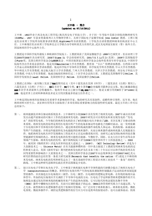
一.压电效应简介当晶体受到某固定方向外力的作用时,内部就产生电极化现象,同时在某两个表面上产生符号相反的电荷;当外力撤去后,晶体又恢复到不带电的状态;当外力作用方向改变时,电荷的极性也随之改变;晶体受力所产生的电荷量与外力的大小成正比。
如果按一定方向对水晶晶体上切下的薄片施加压力,那么在此薄片上将会产生电荷。
如果按相反方向拉伸这一薄片,在此薄片上也会出现电荷,不过符号相反。
挤压或拉伸的力愈大,晶体上的电荷也会愈多。
如果在薄片的两端镀上电极,并通以交流电,那么薄片将会作周期性的伸长或缩短,即开始振动。
在纳米尺度范围内的ZnO线晶体,在(001)或(00-1)方向具有明显的压电性质。
图二为制备的纳米线ZnO晶体阵列。
二.金属-半导体结(MS)及其整流性质的简介。
王中林
王中林– 简介(updated on 07/10/2011)王中林﹐1982毕业于西北电讯工程学院(现名西安电子科技大学)﹐并于同一年考取中美联合招收的物理研究生(CUSPEA)。
1987 年获亚利桑那州立大学物理学博士, 从师于国际电子显微学权威 John Cowley 教授。
王博士现是佐治亚理工学院终身校董事讲席教授,Hightower终身讲席教授,工学院杰出讲席教授和纳米结构表征中心主任。
王中林现任佐治亚理工学院和北京大学联合办学材料系美方首席代表,武汉光电国家实验室(筹)海外主任,国家纳米科学中心海外主任。
王教授是中国科学院外籍院士和欧洲科学院院士。
王教授荣获了美国显微镜学会 1999年巴顿奖章﹐佐治亚理工学院2000和2005年杰出研究奖﹐2005年Sigma Xi 学会持续研究奖,2001年S.T.Li奖金(美国)﹐2009年美国陶瓷学会Purdy奖,美国自然科学基金会CAREER基金﹐中国首批国家自然科学基金会海外优秀青年科学家基金,中国科学院海外杰出学者基金获得者。
他是英国Manchester大学名誉教授,教育部 “长江”特聘讲座教授,台湾国立清华大学晶元讲座教授和名誉讲座教授。
他是科学院半导体所名誉教授, 科学院化学所名誉教授,中山大学名誉教授,华中师范大学名誉教授,南京航天航空大学名誉教授,兰州大学名誉教授,天津大学名誉教授,西安电子科技大学名誉教授,中南大学名誉教授。
他成功地组织和担任过二十次学术会议的主席。
王教授是美国物理学会fellow, 美国科学发展协会(AAAS) fellow,美国材料学会 fellow,美国显微学会fellow。
王教授已在国际一流刊物上发表了700篇期刊论文(其中十篇发表在美国《科学》,三篇发表在《自然》期刊上;六篇发表在《自然》子刊上)﹐45篇书章节﹐36项专利,5本专著和20余本编辑书籍和会议文集。
他已被邀请做过660多次学术讲演和大会特邀报告。
利用压电极化效应实现ZnO回音壁激光模式动态调控
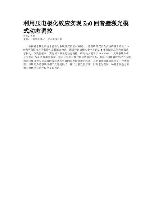
利用压电极化效应实现ZnO回音壁激光模式动态调控
作者:暂无
来源:《科学中国人》 2019年第2期
中国科学院北京纳米能源与系统研究所王中林院士、潘曹峰研究员及卢俊峰博士结合Z n
O光学微腔自身压电特性及其激光模式,通过外部机械应变产生的Z n O谐振腔晶体内部的离
子极化,改变折射率,实现相干激光的动态调控。
研究论文发表于ACS Nano 。
文章系统分析
了应变对ZnO折射率的影响,建立了应变与模式移动的对应关系,获得了超精确度的应力传感,相比较压阻效应引起的能带移动所导致的自发辐射谱的移动,其光谱分辨能力提升了一个数量级。
该研究为动态调控相干光源提供了一种行之有效的方法,同时也为发展一种基于颜色分辨
的应力传感元器件提供了新思路。
Ag修饰的纳米ZnO的合成_表征及光催化特性

Abstract: T he nanopow ders of Z nO and silv er m odif ied Ag/ Z nO are prepared r espect ively by hydrot her mal method and phot osy nt hesis m et hod. T he cry st al st ruct ure and surface m orpho logy of t he samples are charact er ized by X ray diff ract ion ( XRD) and scanning elect ron micr oscopy ( SEM ) . T he phot ocat aly tic act ivity o f t he ZnO and Ag / ZnO nanopow ders is tested by using methy lene blue as t he pollut ant mo del and under the irradiat ion w ith ult raviolet light . T he r esul ts indicat e t hat A g can ef fectively load on ZnO surf ace, and t he pho to cat aly t ic perf orm ance is great ly enhanced by mo dif ication w it h a suit abl e Ag loading. T he pho to cat aly t ic activit y of t he A g/ ZnO w it h Ag loading o f 1 0% is higher than t hat o f ZnO nanopo w der. Wit h 5 0% Ag loading, phot ocat alyt ic activit y is t he highest . H ow ev er, t he phot ocat aly tic act ivity decreases w hen Ag loading is 8 0% . Key words: nano zinc o xide; silver; hy drot hermal m et hod; pho to synt hesis; phot ocat alysis
- 1、下载文档前请自行甄别文档内容的完整性,平台不提供额外的编辑、内容补充、找答案等附加服务。
- 2、"仅部分预览"的文档,不可在线预览部分如存在完整性等问题,可反馈申请退款(可完整预览的文档不适用该条件!)。
- 3、如文档侵犯您的权益,请联系客服反馈,我们会尽快为您处理(人工客服工作时间:9:00-18:30)。
Flexible High-Output Nanogenerator Based on Lateral ZnO Nanowire ArrayGuang Zhu,†Rusen Yang,†Sihong Wang,and Zhong Lin Wang*School of Materials Science and Engineering,Georgia Institute of Technology,Atlanta,Georgia 30332-0245ABSTRACT We report here a simple and effective approach,named scalable sweeping-printing-method,for fabricating flexible high-output nanogenerator (HONG)that can effectively harvesting mechanical energy for driving a small commercial electronic component.The technique consists of two main steps.In the first step,the vertically aligned ZnO nanowires (NWs)are transferred to a receiving substrate to form horizontally aligned arrays.Then,parallel stripe type of electrodes are deposited to connect all of the NWs ing a single layer of HONG structure,an open-circuit voltage of up to 2.03V and a peak output power density of ∼11mW/cm 3have been achieved.The generated electric energy was effectively stored by utilizing capacitors,and it was successfully used to light up a commercial light-emitting diode (LED),which is a landmark progress toward building self-powered devices by harvesting energy from the environment.This research opens up the path for practical applications of nanowire-based piezoelectric nanogeneragtors for self-powered nanosystems.KEYWORDS Nanogenerator,ZnO,nanowire,light-emitting diode,self-poweringEnergy harvesting is critical to achieve independent and sustainable operations of nanodevices,aiming at building self-powered nanosystems.1-3Taking theforms of irregular air flow/vibration,ultrasonic waves,body movement,and hydraulic pressure,mechanical energy is ubiquitously available in our living environment.It covers a wide range of magnitude and frequency from cell contrac-tion to ocean waves.The mechanical-electric energy conver-sion has been demonstrated using piezoelectric cantilever working at its resonating mode.4-7However,the applicabil-ity and adaptability of the traditional cantilever based energy harvester is greatly impeded by the large unit size,large triggering force and specific high resonance frequency.Recently,a series of rationally designed nanogenerators (NGs)with piezoelectric nanowires (NWs)have shown great potentialtoscavengetinyandirregularmechanicalenergy.8-15However,insufficient electric output hinders their practical applications.We report here a simple and effective ap-proach,named scalable sweeping-printing-method,for fab-ricating flexible high-output nanogenerator (HONG).An open-circuit voltage of up to 2.03V and a peak output power density of ∼11mW/cm 3have been achieved.The generated electric energy was effectively stored by utilizing capacitors,and it was successfully used to light up a commercial light-emitting diode (LED),which is a landmark progress toward building self-powered devices by harvesting energy from the environment.Furthermore,by optimizing the density of the NWs on the substrate and with the use of multilayer integra-tion,a peak output power density of ∼0.44mW/cm 2and volume density of 1.1W/cm 3are predicted.The mechanism of converting mechanical energy by a single ZnO NW that is laterally bonded to a substrate has been discussed in details in our previous report.13Owing to much smaller diameter of the NW compared to the substrate thickness,outward bending of the substrate induces a uniaxial tensile strain in the NW.Because of the piezoelectric property of the ZnO NW,the stress results in a piezoelectric field along the length,which causes a transient charge flow in the external circuit.The Schottky contact at the bonded ends can regulate the charge flow.As a result,the bending and releasing of the single-wire-NG gives rise to an alternat-ing flow of the charges in the external circuit.In this work,the power output has been scaled up with the integration of hundreds of thousands of horizontally aligned NWs,which was made by a scalable sweeping-printing-method that is simple,cost-effective,and highly efficient.The method consists of two main steps.In the first step,the vertically aligned NWs are transferred to a receiving substrate to form horizontally aligned arrays.The major components of the transfer setup are two stages (Figure 1a).Stage 1has a flat surface that faces downward and holds the vertically aligned NWs;stage 2has a curved surface and holds the receiving substrate.Polydimethylsiloxane (PDMS)film on the surface of stage 2is used as a cushion layer to support the receiving substrate and enhances the alignment of the transferred NWs.The radius of the curved surface of stage 2equals the length of the rod supporting the stage,which is free to move in circular motion (Supporting Infor-mation Figure S1).In the second step,electrodes are depos-ited to connect all of the NWs together.Vertically aligned ZnO NWs on Si substrates were syn-thesized using physical vapor deposition method.16,17The dense and uniform NWs have the length of ∼50µm,diameter of ∼200nm,and growth direction along the c -axis*To whom correspondence should be addressed.E-mail:zlwang@.†Authors with equal contribution Received for review:6/3/2010Published on Web:07/21/2010(Figure 1b,Supporting Information Figure S2).The same growth direction of NWs guarantees the alignment of the piezoelectric potentials in all of the NWs and a successful scaling up of the output,which will be elaborated later.A small piece of Si substrate with grown ZnO NWs was mounted onto stage 1(Figure 1a)and a piece of Kapton film with the thickness of 125µm was attached to stage 2(Figure 1a).The distance between the receiving substrate and NWs was precisely controlled to form a loose contact between the two.The receiving substrate then counterclockwise swept across the vertical NWs arrays,which were detached from Si substrate and aligned on the receiving substrate along the direction of sweeping due to the applied shear force (Figure 1a).The as-transferred NWs are presented in Figure 2c with an estimated average density of 1.1×106cm -2.The length variation is probably due to the fact that not all of the NWs were broken off at the roots.Next,the evenly spaced electrode pattern over the aligned NWs was first defined using photolithography and thenfollowed by sputtering 300nm thick Au film (Figure 1d).After lifting off the photoresist,600rows of stripe-shaped Au electrodes with 10µm spacing were fabricated on top of the horizontal NW arrays (Figure 1e).Au electrodes form Schottky contacts with the ZnO NWs,which are mandatory for a working NG.8,18Approximately 3.0×10⁵NWs in an effective working area of 1cm 2,as pointed by an arrowhead in Figure 1d (inset),are in contact with electrodes at both ends.Finally,a PDMS packaging over the entire structure can further enhance mechanical robustness and protect the device from invasive chemicals.The working principle of the HONG is illustrated by the schematic diagrams in Figure 2a,b.NWs connected in parallel collectively contribute to the current output;NWs in different rows connected in serial constructively improve the voltage output.The same growth direction of all NWs and the sweeping printing method ensure that the crystal-lographic orientations of the horizontal NWs are aligned along the sweeping direction.Consequently,the polarity ofFIGURE 1.Fabrication process and structure characterization of the HONG.(a)Experimental setup for transferring vertically grown ZnO NWs to a flexible substrate to make horizontally aligned ZnO NW arrays with crystallographic alignment.(b)SEM image of as-grown vertically aligned ZnO NWs by physical vapor method on Si substrate.(c)SEM image of the as-transferred horizontal ZnO NWs on a flexible substrate.(d)Process of fabricating Au electrodes on horizontal ZnO NW arrays,which includes photolithography,metallization,and lift-off.(e)SEM image of ZnO NW arrays bonded by Au electrodes.Inset:demonstration of an as-fabricated HONG.The arrowhead indicates the effective working area of theHONG.the induced piezopotential is also aligned,leading to a macroscopic potential contributed constructively by all of the NWs (Figure 2b).To investigate the performance of the HONG,a linear motor was used to periodically deform the HONG in a cyclic stretching-releasing agitation (0.33Hz).The open-circuit voltage (V oc )and the short-circuit current (I sc )were measured with caution to rule out possible artifacts.19At a strain of 0.1%and strain rate of 5%s -1,peak voltage and current reached up to 2.03V and 107nA,respectively.Assuming that all of the integrated NWs actively contribute to the output,the current generated by a single NW is averaged to be ∼200pA;and the voltage from each row is ∼3.3mV in average.Considering the size of the working area of the nanogenerator (1cm 2)(Figure 1e,inset),a peak output power density of ∼0.22µW/cm 2has been achieved,which is over 20-fold increase compared to our latest report based on a more complex design.14For nanowires with the diameter of ∼200nm,the power volume density is ∼11mW/cm 3,which is 12-22times of that from PZT based cantilever energy harvester.6,7The durability test and further characterization were performed,which prove the stability and robustness of the HONGs (Supporting Information Figure S3).Voltage linear superposition test verified the proposed working principle of the HONGs (Supporting In-formation Figure S4).Further scaling up the power output is expected to be technically feasible.If NWs can be uniformly and densely packed as a monolayer over the entire working area,and all can actively contribute to the output,the maximum power area density is expected to reach ∼22µW/cm 2.The power volume density is anticipated to be improved up to ∼1.1W/cm 3.With 20layers of such NW arrays stacked together,the power area density would be boosted up to ∼0.44mW/cm 2.The performance of the HONG is affected by strain and strain rate.For a given strain rate (5%s -1),an increase in strain leads to a larger output (Figure 3a,b).Likewise,at a constant strain (0.1%),the output is proportional to the strain rate (Figure 3c,d).Beyond a certain strain and strain rate,saturation of the magnitude occurs,probably due to the converse piezoelectric effect,which is the strain created by the piezopotential and it is opposite to the externally induced strain.It is noticed that 0.1%strain is sufficient to induce effective output,which is much smaller than the 6%fracture strain of the ZnO NW predicted theoretically.20Storing the generated energy and driving functional devices are extremely important steps toward practical applications of the nanogenerator.In this work,they were accomplished by using a charging-discharging circuit with two consecutive steps (Figure 4).The circuit function is determined by the status of a switch (Figure 4a inset).TheFIGURE 2.Working principle and output measurement of the HONG.(a)Schematic diagram of HONG’s structure without mechanical deformation,in which gold is used to form Schottky contacts with the ZnO NW arrays.(b)Demonstration of the output scaling-up when mechanical deformation is induced,where the “(”signs indicate the polarity of the local piezoelectric potential created in the NWs.(c)Open circuit voltage measurement of the HONG.(d)Short circuit current measurement of the HONG.The measurement is performed at a strain of 0.1%and strain rate of 5%s -1with the deformation frequency of 0.33Hz.The insets are the enlarged view of the boxed area for one cycle ofdeformation.switch is at position A for energy storage achieved by charging capacitors.Upon charging completion,the switch is switched to position B for energy releasing to power a functional device,such as a light emitting diode.It is the key for a successful and effect energy storage to take full advantage of the alternating output.As a result,an integrated full wave rectifying bridge (Transys Electronics Limited,DI 102)was connected between a HONG andFIGURE 3.Performance characterization of the HONG with increasing strain and strain rate.(a)Open circuit voltage measurement of the HONG with increasing strain at a given strain rate of 5%s -1.(b)Short circuit current measurement of the HONG with increasing strain at a given strain rate of 5%s -1.(c)Open circuit voltage measurement of the HONG with increasing strain rate at a constant strain of 0.1%.(d)Short circuit current measurement of the HONG with increasing strain rate at a constant strain of 0.1%.For all measurements,the mechanical deformation frequency is fixed at 0.33Hz.FIGURE 4.Application of the electric energy generated by the HONG to drive a commercial light emitting diode.(a)The electric output measured after a full wave rectifying bridge.Signals of negative signs are reversed,as pointed by the arrowhead.Inset:Schematic of the charging-discharging circuit for storing and releasing the energy generated by the HONG,respectively.(b)Image of a commercial LED,which is incorporated into the circuit.(c)Image of the LED in dim background before it was lit up.(d)Image of the LED in dim background at the moment when it was lit up by the energy generated from theHONG.capacitors(Vishay Sprague,Type430P,2µF(10%).The output of the HONG measured after the bridge exhibits only positive signals(Figure4a).Full wave rectification achieved by the bridge ensures energy storage at an enhanced ef-ficiency,although the rectified signal(as pointed by an arrowhead in Figure4a)has appreciably reduced magnitude due to the reverse current leakage of the diodes in the bridge; this reducing effect is rather notable at small output current. To facilitate the charging process,the output frequency of the HONG was tuned up to3Hz by reducing the periodicity of the mechanical deformation.Ten capacitors were con-nected in parallel such that they were simultaneously charged, and the voltage across a single capacitorfinally reached0.37 V.Uponfinishing charging,the capacitors were reconfigured from parallel connection to series connection,leading to a total voltage source of3.7V.The stored electricity was used to drive a commercial red LED(Figure4b,Avago Technolo-gies US Inc.,HLMP-1700),which has an emission spectrum centered at635nm.The turn-on voltage and forward-biased resistance are1.7V and450Ω,respectively.The discharg-ing process was triggered,leading to a maximum discharg-ing current of4.5mA and the LED was lit up.The emitted light lasted0.1-0.2s and was clearly captured in dim background(Figure4c,d,video in Supporting Information). During the whole charging-discharging process,no other power sources were involved.The entire circuit is essentially a complete self-powered system,which consists of three components:an energy harvester(the HONG),storage units (capacitors),and a functional device(the LED).An effective energy generation efficiency is defined as the ratio between the energy stored by the capacitors and the strain energy input to all of the active NWs,and it takes into account the performance of the electronic components in the circuit.The total electrical energy stored by the capacitor can be calculated as W stored)CU2n/2)1.37µJ,where C is the capacitance of a single capacitor,U is voltage across the capacitor,and n is the number of capacitors.Since the dominant strain in the ZnO NWs is tensile strain,with shear strain safely neglected,the total strain energy can be esti-mated as W strain)πD2L0Eε2ftn0/8)30µJ,where D is the diameter of the NW(200nm),L0is its original length(10µm),which isfixed by the electrode spacing,E is the Young’s modulus(30GPa),εis the strain of NWs(0.1%),f is the frequency of deformation(3Hz),t is the total charging time (7200s),and n0is the number of integrated NWs (300000).13Therefore,the effective energy generation ef-ficiency is estimated to be∼4.6%.This value is naturally lower than the energy conversion efficiency of a single nano/ microwire(∼7%),which is defined as the ratio between the generated electric energy(W generated)∫VI d t,where V is the voltage,and I is the current)and the mechanical input strain energy.13This is mainly attributed to the energy dissipation on rectifying bridge and capacitors,as elaborated in the Supporting Information.In summary,we have successfully fabricated high-output flexible nanogenerators using a sweeping-printing method. We managed to transfer vertically grown ZnO NWs to a flexible substrate and achieved horizontally aligned NW arrays that have crystallographic alignment,based on which an innovatively designed HONG was fabricated.The electri-cal output of the HONG reached a peak voltage of2.03V and current of107nA with a peak power density of∼11 mW/cm3,which is12-22times of that from PZT-based cantilever energy harvester.An effective energy generation efficiency of4.6%was demonstrated.The electric energy generated by the HONG was effectively stored by capacitors and used to light up a commercial LED.Furthermore,by optimizing the density of the NWs on the substrate and with the use of multilayer integration,a peak output power density of∼0.44mW/cm2and volume density of1.1W/c m3 are redicted.This is a key step that is likely to bring nanogenerator based self-powering technology into people’s daily life with potential applications in mobile electronics, health monitoring,environmental inspection,cargo shipping tracking system,infrastructure monitoring,and even de-fense technology.Acknowledgment.Research supported by NSF(DMS 0706436,CMMI0403671,ENG/CMMI112024),DARPA (Army/AMCOM/REDSTONE AR),BES DOE(DE-FG02-07ER46394),and DARPA/ARO W911NF-08-1-0249.The authors thank Cheng Li and Benjamin Hansen for their help on thinfilm deposition and electric circuit design,respectively. Supporting Information Available.Experimental setup, additionalfigures,and video.This material is available free of charge via the Internet at . REFERENCES AND NOTES(1)Wang,Z.L.Sci.Am.2007,298,82–87.(2)Tian,B.Z.;et al.Nature2007,449,885–890.(3)Pan,C.F.;et al.Adv.Mater.2008,20,1644–1648.(4)Hausler,E.;et al.Ferroelectronics1984,60,277–282.(5)Platt,S.R.;et al.IEEE-ASME T.Mech.2005,10,455–461.(6)Round,S.;Wright,P.K.;Rabaey,mun.2003,26,1131–1144.(7)Shen,D.N.;et al.Sens.Actuators,A2009,154,103–108.(8)Wang,Z.L.;Song,J.H.Science2006,312,242–246.(9)Wang,X.D.;Song,J.H.;Liu,J.;Wang,Z.L.Science2007,316,102–105.(10)Chang,C.;Tran,V.H.;Wang,J.;Fuh,Y.;Lin,L.Nano Lett.2010,10,726–731.(11)Qin,Y.;Wang,X.D.;Wang,Z.L.Nature2008,451,809–813.(12)Qi,Y;et al.Nano Lett.2010,10,524–528.(13)Yang,R.;Qin,Y.;Dai,L.;Wang,Z.L.Nat.Nanotechnol.2009,4,34–39.(14)Xu,S.;Qin,Y.;Xu,C.;Wei,Y.G.;Yang,R.;Wang,Z.L.Nat.Nanotechnol.2010,5,367–273.(15)Choi,D.;et al.Adv.Mater.2010,22,2187–2192.(16)Pan,Z.W.;Dai,Z.R.;Wang,Z.L.Science2001,291,1947–1949.(17)Kuo,T.;et al.Chem.Mater.2007,19,5143–5147.(18)Polyakov,A.Y.;et al.Appl.Phys.Lett.2003,83,1575–1577.(19)Yang,R.;Qin,Y.;Li,C.;Dai,L.;Wang,Z.L.Appl.Phys.Lett.2009,94,No.022905.(20)Agrawal,R.;Peng,B.;Espinosa,H.D.Nano Lett.2009,9,4177–4183.。