Smart CMOS Focal Plane Arrays A Si CMOS Detector Array and Sigma–Delta Analog-to-Digital C
CMOS-APS的优点和设计方法

CMOS-APS的优点和设计方法
1.CMOS-APS胜过CCD图像传感器的潜在优点
CMOS APS胜过CCD图像传感器的潜在优点包括[1]~[3]:
1)消除了电荷反复转移的麻烦,免除了在辐射条件下电荷转移效率(CTE)的退化和下降。
2)工作电流很小,可以防止单一振动和信号闭锁。
3)在集成电路芯片中可进行信号处理,因此可提供芯迹线,模/数转换的自调节,也能提供由电压漂移引起的辐射调节。
与硅探测器有关,需要解决的难题和争论点包括[1]~[3]:
1)在体材料界面由于辐射损伤而产生的暗电流的增加问题。
2)包括动态范围损失的阈值漂移问题。
3)在模/数转换电路中,定时和控制中的信号闭锁和单一扰动问题。
2.CMOS-APS的设计方法
CMOS-APS的设计方法包括:
1)为了降低暗电流而进行研制创新的像素结构。
2)使用耐辐射的铸造方法,再研制和开发中等尺寸“dumb”(哑)成像仪(通过反复地开发最佳像素结构)。
3)研制在芯片上进行信号处理的器件,以适应自动调节本身电压Vt的漂移和动态范围的损失。
4)研制和开发耐辐射(单一扰动环境)的定时和控制装置。
5)研制和加固耐辐射的模/数转换器。
6)寻找低温工作条件,以便在承受最大幅射强度时,找到并证
实最佳的工作温度。
7)研制和开发大尺寸、全数字化、耐辐射的CMOS-APS,以便生产。
8)测试、评价和鉴定该器件的性能。
9)引入当代最高水平的组合式光学通信/成像系统测试台。
图像处理(Image processing)

ELEC 319/419
Image Processing
ELEC 319/419
ImagPlane
• The focal plane of a (Charge Coupled Device – CCD) digital camera is laid out as shown in the diagram. • •
Photo-diodes & Pixels
• Light (photons) falling on the photo-sensitive area are converted into an electronic signal. The photon is absorbed creating an electronhole pair, the hole drifts to the ground electrode and is removed and the electron is held by the gate electrode (in positive bias detectors).
•
CMOS Systems
– The charge-to-voltage conversion occurs in each pixel and the voltages and can be read out one by one. – This results in a more flexible device (can select a small area from the whole focal plane – ‘windowing in’) faster frame rates for reduced images and lower power consumption. – However, the pixel area is shared between the detector and the circuitry so some compromise is required – more complex circuitry and smaller pixel area = fewer photons/smaller signals.
CMOS设置及图解
CMOS设置及图解流浪的羽毛发表于2007-5-12 23:56:00BIOS(basic input output system 即基本输入输出系统)设置程序是被固化到计算机主板上的R OM芯片中的一组程序,其主要功能是为计算机提供最底层的、最直接的硬件设置和控制。
BIOS 设置程序是储存在BIOS芯片中的,只有在开机时才可以进行设置。
CMOS主要用于存储BIOS设置程序所设置的参数与数据,而BIOS设置程序主要对技巧的基本输入输出系统进行管理和设置,是系统运行在最好状态下,使用BIOS设置程序还可以排除系统故障或者诊断系统问题。
在我们计算机上使用的BIOS程序根据制造厂商的不同分为:AWARD BIOS程序、AMI BIOS 程序、PHOENIX BIOS程序以及其它的免跳线BIOS程序和品牌机特有的BIOS程序,如IBM等等。
目前主板BIOS有三大类型,即AWARD AMI和PHOENIX三种。
不过,PHOENIX已经合并了AWARD,因此在台式机主板方面,其虽然标有AWARD-PHOENIX,其实际还是AWARD的B IOS的. Phoenix BIOS 多用于高档的586原装品牌机和笔记本电脑上,其画面简洁,便于操作。
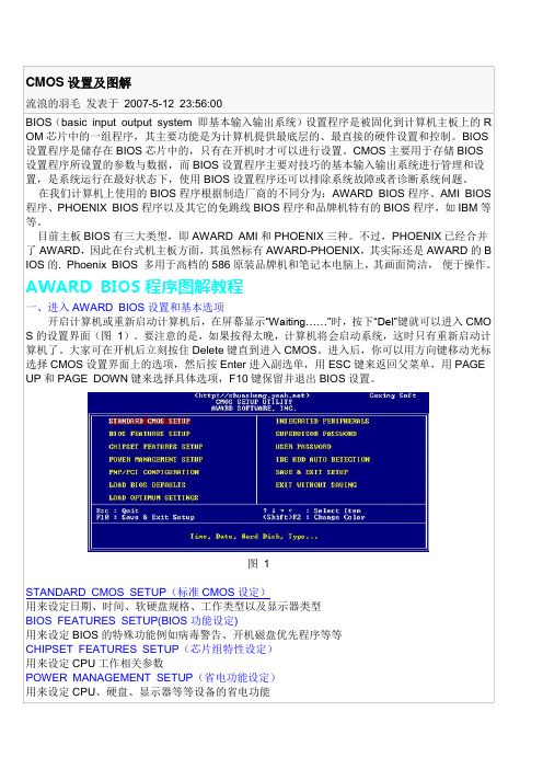
AWARD BIOS程序图解教程一、进入AWARD BIOS设置和基本选项开启计算机或重新启动计算机后,在屏幕显示“Waiting……”时,按下“Del”键就可以进入CMO S的设置界面(图1)。
要注意的是,如果按得太晚,计算机将会启动系统,这时只有重新启动计算机了。
大家可在开机后立刻按住Delete键直到进入CMOS。
进入后,你可以用方向键移动光标选择CMOS设置界面上的选项,然后按Enter进入副选单,用ESC键来返回父菜单,用PAGE UP和PAGE DOWN键来选择具体选项,F10键保留并退出BIOS设置。
图 1STANDARD CMOS SETUP(标准CMOS设定)用来设定日期、时间、软硬盘规格、工作类型以及显示器类型BIOS FEATURES SETUP(BIOS功能设定)用来设定BIOS的特殊功能例如病毒警告、开机磁盘优先程序等等CHIPSET FEATURES SETUP(芯片组特性设定)用来设定CPU工作相关参数POWER MANAGEMENT SETUP(省电功能设定)用来设定CPU、硬盘、显示器等等设备的省电功能PNP/PCI CONFIGURATION(即插即用设备与PCI组态设定)用来设置ISA以及其它即插即用设备的中断以及其它差数LOAD BIOS DEFAULTS(载入BIOS预设值)此选项用来载入BIOS初始设置值LOAD OPRIMUM SETTINGS(载入主板BIOS出厂设置)这是BIOS的最基本设置,用来确定故障范围INTEGRATED PERIPHERALS(内建整合设备周边设定)主板整合设备设定SUPERVISOR PASSWORD(管理者密码)计算机管理员设置进入BIOS修改设置密码USER PASSWORD(用户密码)设置开机密码IDE HDD AUTO DETECTION(自动检测IDE硬盘类型)用来自动检测硬盘容量、类型SAVE&EXIT SETUP(储存并退出设置)保存已经更改的设置并退出BIOS设置EXIT WITHOUT SAVE(沿用原有设置并退出BIOS设置)不保存已经修改的设置,并退出设置图 2STANDARD CMOS SETUP(标准CMOS设定)图2标准CMOS设定中包括了DATE和TIME设定,您可以在这里设定自己计算机上的时间和日期。
工业相机特性介绍及其差异

工业相机特性介绍及其差异关键词:工业相机,ccd数字工业相机,图像处理,CMOS数字工业相机,B looming 效应,S mear效应当前应用最广泛的数字工业相机有CCD 数字工业相机和CMOS 数字工业相机两大类。
CCD 数字工业相机CCD 是电荷藕合器件(Charge Coupled Device)的简称,它是应用最广泛的图像传感器之一。
一个CCD 图像传感器是成像像元为X-Y 纵横矩阵排列,每个成像像元由一个光电二极管和其控制的一个相邻电荷存储区组成。
光电二极管将光线(光子)转换为电荷(电子),电荷存储区收集到的电子总数量与光线的强度成正比。
在读取这些电荷时,各列电荷存储区收集到的光生电子被移动到垂直电荷传输方向的电荷传递寄存器中,然后各列电荷传递寄存器中的电荷按行被移到总的行电荷传递寄存器中,总的行电荷传递寄存器中每行的电荷信息再被连续读出,通过同一电荷/电压转换器和放大器来生成图像信息。
当光强不太强时,CCD传感器的响应是线性的,CCD 像元内的电荷存储区可以存储全部光电荷,此为线性范围。
当光强继续增大时,因为电荷存储区已存储了很多光生电荷,由光生电荷产生的电场会妨碍像元按线性继续积累电荷,CCD 便进入了饱和区。
如果光强进一步增大,电荷存储势阱将填满电子,而过剩的电子会向外溢出。
如果没有特殊措施,溢出的电子将进入相邻像素,致使本来工作在线性区域的相邻像素在收集到溢出电子后进入饱和区或也向外溢出电子,使图像出现光晕现象,图像清晰度也就明显下降了。
CCD 图像传感器的原理和结构使其有较好光照灵敏度高、噪音低、图象质量较高的优点,一般CCD 工业相机的动态范围在60dB 左右。
但在图像中有高亮度的点或区域时,CCD 图像传感器存在让图像质量严重劣化的“Blooming”和“Smear”效应。
CMOS 数字工业相机CMOS 是Complimentary Metal Oxide Semiconductor (互补型金属氧化半导体)的简称,CMOS 和CCD 传感器一样,是在Si(硅)半导体材料上制作的。
红外成像信号检测技术

红外成像信号检测技术(Signal Detection Technology of Infrared Imaging)王欢王志功冯军(Wanghuan Wang Zhigong Fengjun)(东南大学射频与光电集成电路研究所南京四牌楼2号 210096)摘要:介绍了红外成像技术的发展及现状,二维混合红外焦平面阵列(IR FPAs)的基本概念和单元结构,并结合BDI和CTIA两种读取电路对红外成像信号检测技术的工作原理进行了阐述。
关键词:红外焦平面阵列,检测器,读取电路关键词Abstract This paper introduces the development and prensent situation of infrared imaging technology.The conception and cell structure of hybrid infrared facal-plane arrays of two dimentions are presented too.This paper also discusses the characteristic of signal detection technology based on the BDI and CTIA.Key Words facal-plane arrays, detector, readout circuit红外成像系统大体可分为三代:第一代装置是把单个传感元件和对空间目标进行二维扫描的扫描镜组合在一起,获得红外图像。
3—5µm的红外传感器有HgCdTe光电导型(PC 型:photoconductive)和InSb光电型(PV型:photovoltaic)。
8—14µm的是HgCdTe光电导型。
第二代装置把一维传感器阵列和一维扫描镜组合在一起,多采用PC型HgCdTe传感器阵列。
现在PC型HgCdTe元件的灵敏度已大体接近BLIP(background limited infrared photo conductor)状态,要提高系统的分辨率,可采用TDI(time delay and integration:时间延迟积分)技术,提高信噪比。
索尼 Alpha 6100 数字单反相机说明书

Key Features24.2MP 2 and incredible image qualityThe Alpha 6100 boasts an impressive APS-C image sensor with approximately 24.2 effective megapixels, the latest BIONZ X™ image processing engine and the same front end LSI as used on Sony’s acclaimed full-frame cameras to deliver outstanding image quality with rich detail and true-to-life color reproduction. Area specific noise reduction results in low noise even at high ISO which ranges from 100 – 32,000 (Expandable up to ISO – 51,200). The design significantly increases readout speed, enabling functionality including 11fps continuous shooting 5, 4K recording 3 with full pixel readout without pixel binning and Full HD 120fps high-speed shooting.Superior autofocus with 4D FOCUS™The Alpha 6100 incorporates Sony’s unrivaled 4D FOCUS™ system for unsurpassed fast autofocus (AF) acquisition time that can lock focus on even the fastest moving subject in as little as 0.02 seconds 1. It also boasts an incredible 425 phase detection and 425 contrast detection AF points that are densely positioned over 84% of the image area, effectively tracking subjects as they move across the frame. Moreover, the Alpha 6600 takes full advantage of its enhanced fast hybrid AF for movies in both HD and 4K 3. Both AF detection accuracy and tracking performance have been boosted.Advanced Real-time Eye AF, humans and animals 6Advanced “Real-time Eye AF 6” employs (Ai) artificial intelligence, including machine learning , to detect and process eye data in real time, resulting in improved accuracy, speed and tracking performance of Eye AF. Eye AF can be employed for humans, animals 6 and when recording movie. With a half press of the shutter button, the camera can automatically detect the eyes of the subject and activate Eye AF in all autofocus modes. When in either AF-C or AF-A mode, eye capture is continuously maintained. Additionally, the preferred eye (right or left) of your subject can be selected as the focus point. Choices include Auto/Right Eye/Left Eye, and a Switch Right/Left Eye function is assignable to a custom function or the touchscreen panel.Real-time Tracking Autofocus“Real-time Tracking” is a state-of-the-art feature that utilizes a special object recognition algorithm that processes color, subject distance (depth), brightness (pattern) as spatial information, plus AI (Artificial Intelligence with machine learning) information including face and eye location, ensuring that all subjects can be captured with extreme accuracy and precision. This can be activated by a simple half press of the shutter button, or can be assigned to a custom function as well. The subject to be tracked can also be specified by touching it on the monitor when the Touch Tracking function is engaged.Real-time Eye AF for animals 6Advanced AI-based subject recognition technology now allows fast, precise, automatic detection and tracking of animal 6 eyes. This new capability can vastly increase success rates when photographing animals in a variety of settings or pets at home. Real-time Eye AF animal mode can be initiated either by pressing an assigned custom button or by half-pressing the shutter button.16-bit processing and 14-bit RAW outputImage sensor output is processed in 16-bit form by the front-end LSI and BIONZ X image processing engine before being output as compressed or uncompressed 14-bit RAW files that have smoother, more natural gradations for higher overall image quality. 14-bit RAW output is available even when shooting in silent or continuous mode.Up to 11fps 5 at 24.2MP with AE/AF trackingILCE-6100/BAlpha 6100 APS-C Mirrorless Interchangeable-LensCameraThe Alpha 6100 include a 24.2MP 2 Exmor™ CMOS image sensor, the latest BIONZ X™ image processor and a front-end LSI as implemented in Sony’s full-frame cameras, which combine to deliver all-round enhancements in image quality and performance across all areas of photo and video capture.The Alpha 6100 has been designed to allow for high resolution, continuous shooting at high frame rates. It features a front-end LSI that works with the image sensor, BIONZ X image processing engine and a newly designed shutter mechanism with ‘braking feature’ to enable continuous shooting at impressive speeds up to 11fps5 with continuous autofocus and auto-exposure tracking at full 24.2MP resolution while utilizing the mechanical shutter, and up to 8 fps5 with full AF/AE tracking while silent shooting.4K movie3 w/ full pixel readout, no pixel binningThe Alpha 6100 offers internal 4K (QFHD: 3840 x 2160) recording3 in Super 35mm format with full pixel readout and no pixel binning at 2.4x oversampling4 (6K equivalent) for the ultimate 4K footage with exceptional detail and depth. Additional the Alpha 6100 has the ability to record Full HD at 120 fps for up to 5x slow motion HD video7 and a mic jack with XLR compatibility via the MI shoe, focus peaking, clean HDMI output and much more.Touch Tracking for moviesTouch Tracking is beneficial for movie recording. Touch the subject to be tracked on the monitor, and the Real-time Tracking function will then process color, pattern (brightness), distance (depth), and face information to precisely and smoothly track the selected subject at the specified sensitivity and speed. It is also possible to half-press the shutter button or press the AF ON button while shooting to achieve fast focus (AF-S). This can be an advantage for weddingsor documentaries, where there is only one chance to capture a scene. In such cases the focus area selected in advance is applied.180-degree tiltable LCD touch screen for self-recordingThe fully tiltable (180-degree), 3” (3.0-type) LCD flip screen with 921k-dots of high-resolution allows for simple and effective selfie-style shooting for both still image and video capture. Utilizing this capability, vloggers will be able to check and monitor composition throughout their entire creative process. The LCD screen is also equipped with touch functionality, with options for Touch Pad, Touch Focus, Touch Shutter and new Touch Tracking which quickly activates “Real-time Tracking” through the touch screen.Wi-Fi®/NFC™/QR code for easy file transfer and remote control8Easily connect with NFC or QR code (for non-NFC devices) to smartphones or tablets with the built-in Wi-Fi® and Sony’s PlayMemories Mobile™ application available for free on the Android™ and iOS platforms8. Control your camera or transfer files to your device for fast and easy sharing without the need of a computer. It also supports Sony’s growing range of PlayMemories Camera Apps™, which add a variety of creative capabilities to the camera. Then when you’re done, you can use the free software to sort and manage your stills and video with PlayMemories Home™ or edit your RAW file with either Sony’s Image Data Converter or Capture One Express (for Sony). Make it your own with easy button and dial customizationMake operation more intuitive, quick and easy. You can assign any of 89 functions to any of 8 custom buttons. Independent function sets can be assigned for stills, movies, and playback. “My Dial” allows for frequently-used functions to be assigned to the control dial and control wheel. The My Menu function allows up to 30 frequently-used menu items to be registered. They can be re-ordered by frequency of use, and little-used items can be deleted, allowing the user to create a menu that reflects their usage patterns.Interval Recording7 for time-lapseInterval shooting7 (continuous shooting with a set interval) is possible to create time-lapse movies, without requiring an app or external interferometer. Shooting interval can be set to anywhere between 1 second and 60 seconds, and the number of shots to anywhere from 1 to 9999. AE tracking sensitivity can be set to ”High”, “Mid” or “Low” during interval shooting to control your exposure and silent shooting can be activated to reduce shutter vibration. To extend shooting periods, a mobile battery can be used while the internal battery remains in the camera. Still images shot can be edited into a time-lapse movie on a computer with the latest version of Imaging Edge software (Remote/Viewer/Edit) and PlayMemories Home.Slow and quick motion7Slow and quick motion7 offers an almost endless variety of creative ways to express the passage of time. Frame rates from 1 fps to 120fps (100fps) can be selected in eight steps for full HD up to 50 Mbps; 60x quick motion/5x slow in NTSC and 50x quick motion/4x slow in PAL.4K movie transfer to smartphone8By using the newly introduced smartphone app Imaging Edge Mobile, high-bitrate movies including 4K can be transferred to smartphones (Probability of transfer / playback depends on the performance of the smartphone). Refer to the product information for Imaging Edge Mobile for detailsImaging Edge desktop applicationsTo support an efficient, high speed, connected professional workflow, Sony provides “Imaging Edge” desktop applications. Use "Remote" to control and monitor shooting live on your PC screen; "Viewer" to quickly preview, rate, and select photos from large image libraries; and "Edit" to develop RAW data into high-quality photos for delivery. Get the best from Sony RAW files, and manage your productions more efficiently. To maximize convenience in image transfer, when utilizing the latest version of Sony’s Imaging Edge Mobile™ application, the camera can now transfer images to a connected smartphone even if the camera’s power is set to OFF. Refer to the download page for details: /disoft/d/Specifications1. Based on Sony research, CIPA-guideline-compliant internal measurement with an E 18-135mm F3.5-5.6 OSS lens mounted, Pre-AF off and viewfinder in use.2. Approximately, effective megapixels3. 3840×2160 pixels. A Class 10 or higher SDHC/SDXC memory card is required to record movies in the XAVC S format. UHS-I (U3) SDHC/SDXC card is required for 100Mbps4. Standard ISO 100 up to ISO 32000 expandable to ISO 100 to ISO 51200for still images5. High-speed continuous shooting is available at up to approx. 11fps in “Hi+” continuous shooting mode and up to approx. 8fps in “Hi” continuous shooting mode. Maximum fps will depend on camera settings.6. Accurate focus may not be achieved with certain subjects in certain situations.. Real-time Eye AF for Animals supports still images only and cannot be used in combination with tracking. Does not work with some types of animal.7. Wi-Fi does not work during interval shooting8. Imaging Edge Mobile Ver. 7.2 or later is required© 2019 Sony Electronics Inc. All rights reserved. Reproduction in whole or in part without written permission is prohibited. Sony is not responsible for typographical and photographic errors. Features and specifications are subject to change without notice. Sony, G Master, the Alpha logo and the Sony logo are trademark of Sony Corporation. All other trademarks are trademarks of their respective owners.。
小像元间距、晶圆级封装、asi

小像元间距、晶圆级封装、asi1.小像元间距是数字图像处理中的重要参数。
The pixel pitch is an important parameter in digital image processing.2.晶圆级封装可以提高集成电路的稳定性。
Wafer-level packaging can improve the stability of integrated circuits.3. asi技术在半导体制造中有着广泛的应用。
Advanced Silicon Integration (ASI) technology has a wide range of applications in semiconductor manufacturing.4.微探测器的小像元间距决定了其空间分辨率。
The small pixel pitch of micro detectors determines their spatial resolution.5.晶圆级封装可以有效减少集成电路的尺寸。
Wafer-level packaging can effectively reduce the size of integrated circuits.6. asi技术可以提高半导体器件的性能和可靠性。
ASI technology can improve the performance andreliability of semiconductor devices.7.晶圆级封装可以降低集成电路的成本。
Wafer-level packaging can reduce the cost of integrated circuits.8.小像元间距越小,图像的清晰度就越高。
The smaller the pixel pitch, the higher the image resolution.9. asi技术的发展推动了半导体产业的进步。
ARRI ALEXA Mini LF 摄影机说明书

Identity Number K1.0024074Model ALEXA Mini LFSensor Type Large Format ARRI ALEV III (A2X) CMOS sensor with Bayer pattern colorfilter arraySensor Maximum Resolution and Size4448 x 309636.70 x 25.54 mm / 1.444 x 1.005"⌀ 44.71 mm / 1.760"Sensor Frame Rates0.75 - 90 fpsWeight∼2.6 kg / ∼5.7 lbs(camera body with LPL lens mount)800 g (MVF-2)Photosite Pitch8.25 μmSensor Active Image Area Photosites LF Open Gate ProRes 4.5K: 4448 x 3096LF Open Gate ARRIRAW 4.5K: 4448 x 3096LF 16:9 ProRes HD: 3840 x 2160LF 16:9 ProRes 2K: 3840 x 2160LF 16:9 ProRes UHD: 3840 x 2160LF 16:9 ARRIRAW UHD: 3840 x 2160LF 2.39:1 ProRes 4.5K: 4448 x 1856LF 2.39:1 ARRIRAW 4.5K: 4448 x 1856Sensor Active Image Area Dimensions LF Open Gate ProRes 4.5K: 36.70 x 25.54 mm / 1.445 x 1.006"LF Open Gate ARRIRAW 4.5K: 36.70 x 25.54 mm / 1.445 x 1.006"LF 16:9 ProRes HD: 31.68 x 17.82 mm / 1.247 x 0.702"LF 16:9 ProRes 2K: 31.68 x 17.82 mm / 1.247 x 0.702"LF 16:9 ProRes UHD: 31.68 x 17.82 mm / 1.247 x 0.702"LF 16:9 ARRIRAW UHD: 31.68 x 17.82 mm / 1.247 x 0.702"LF 2.39:1 ProRes 4.5K: 36.70 x 15.31 mm / 1.445 x 0.603"LF 2.39:1 ARRIRAW 4.5K: 36.70 x 15.31 mm / 1.445 x 0.603" Recording File Container Size LF Open Gate ProRes 4.5K: 4480 x 3096LF Open Gate ARRIRAW 4.5K: 4448 x 3096LF 16:9 ProRes HD: 1920 x 1080LF 16:9 ProRes 2K: 2048 x 1152LF 16:9 ProRes UHD: 3840 x 2160LF 16:9 ARRIRAW UHD: 3840 x 2160LF 2.39:1 ProRes 4.5K: 4480 x 1856LF 2.39:1 ARRIRAW 4.5K: 4448 x 1856Recording File Image Content LF Open Gate ProRes 4.5K: 4448 x 3096LF Open Gate ARRIRAW 4.5K: 4448 x 3096LF 16:9 ProRes HD: 1920 x 1080LF 16:9 ProRes 2K: 2048 x 1152LF 16:9 ProRes UHD: 3840 x 2160LF 16:9 ARRIRAW UHD: 3840 x 2160LF 2.39:1 ProRes 4.5K: 4448 x 1856LF 2.39:1 ARRIRAW 4.5K: 4448 x 1856Exposure Latitude14+ stops over the entire sensitivity range from EI 160 to EI 3200 asmeasured with the ARRI Dynamic Range Test Chart (DRTC-1) Exposure Index Adjustable from EI 160-3200 in 1/3 stopsEI 800 base sensitivityShutter Electronic shutter, 5.0°- 356° or 1s - 1/8000sRecording Formats MXF/ARRIRAWMXF/Apple ProRes 4444 XQMXF/Apple ProRes 4444MXF/Apple ProRes 422 HQRecording Media Codex Compact DrivesRecording Frame Rates LF Open Gate ProRes 4.5K: 0.75 - 40 fpsLF Open Gate ARRIRAW 4.5K: 0.75 - 40 fpsLF 16:9 ProRes HD: 0.75 - 90 fpsLF 16:9 ProRes 2K: 0.75 - 90 fpsLF 16:9 ProRes UHD: 0.75 - 60 fpsLF 16:9 ARRIRAW UHD: 0.75 - 60 fpsLF 2.39:1 ProRes 4.5K: 0.75 - 60 fpsLF 2.39:1 ARRIRAW 4.5K: 0.75 - 60 fpsNote: maximum fps values are preliminary informationRecording Modes Standard real-time recordingNo Pre-recordingNo IntervalometerViewfinder Type Multi Viewfinder MVF-2 with 4" flip-out monitorViewfinder Technology OLED viewfinder displayLCD fold out monitorViewfinder Resolution Pixel1920 x 1080Viewfinder Diopter Adjustable from -5 to +5 dioptersColor Output Rec 709Rec 2020Log CCustom Look (ARRI Look File ALF-2)Look Control Import of custom 3D LUTASC CDL parameters (slope, offset, power, saturation)White Balance Manual and auto white balance, adjustable from 2000K to 11000K in 10KstepsColor correction adjustable range from -16 to +16 CC1 CC corresponds to 035 Kodak CC values or 1/8 Rosco valuesFilters Built-in motorized ND filters 0.6, 1.2, 1.8Fixed optical low pass, UV, IR filterImage Outputs 1x proprietary signal output for MVF-2 viewfinder on VF CoaXPressconnector (video, audio, power, control signals)SDI 1:-HD only, Processed or Clean, with or without a look file applied-1.5G 422 HD (SMPTE ST292-1, up to 30 fps, progessive (p) or progressivesegmented frame (psf))-3G 422 HD (SMPTE ST425-1, up to 60 fps, p)-3G 444 HD (SMPTE ST425-3, up to 30 fps, p)SDI 2:-HD or UHD, Clean only, with or without a look file applied, or SDI 1 clone-1.5G 422 HD (SMPTE ST292-1, up to 30 fps, p or psf)-3G 422 HD (SMPTE ST425-1, up to 60 fps, p)-3G 444 HD (SMPTE ST425-3, up to 30 fps, p)-6G 422 UHD (SMPTE ST2081-10, up to 30 fps, p)“Clean” is an image without surround view or overlays (status, false color,zebra, framelines, etc.)“Processed” is an image with surround view or overlays.Lens Squeeze Factors 1.001.251.301.501.651.802.00Exposure and Focus Tools False ColorZebraZoomAperture and Color PeakingAudio Input1x LEMO 6pin balanced stereo line in with 12V power output(Line input max. level +24dBu correlating to 0dBFS)Audio Output SDI (embedded)3,5mm stereo headphone jack (on MVF-2)Audio Recording 2 channel linear PCM, 24 bit 48 kHzRemote Control Options MVF-2 viewfinder can act as wired remote control with 10m/33ft cableWeb-based remote control from smart phones, tablets and laptops viaWiFi & Ethernet (beta version)Camera Access Protocol (CAP) via Ethernet & WiFiGPIO interface for integration with custom control interfacesWCU-4 hand-unit with control over lens motors and operationalparameters via built-in white radioSXU-1 hand-unit with control over one lens channelOCU-1 and Master Grip control of lens and user buttonsInterfaces1x LEMO 5pin LTC Timecode In/Out1x LEMO 10pin Ethernet for remote control and service1x BNC SYNC IN1x LEMO 7pin EXT multi purpose accessory interface w. RS pin and 24Vpower output1x LEMO 4pin LBUS (on lens mount) for lens motors, daisy chainable1x USB 2.0 in media bay (for user setups, look files etc)Wireless Interfaces Built-in WiFi module (IEEE 802.11b/g)Built-in White Radio for ARRI lens and camera remote controlLens Mounts LPL lens mount with LBUS connectorPL-to-LPL adapterLeitz M mount (available from Leitz)Flange Focal Depth LPL mount: 44 mmwith PL-to-LPL adapter: 52 mmPower Input1x LEMO 8pin (11-34 V DC)Power Consumption Around 65 W when recording ARRIRAW at 24 fps with MVF-2 attached(preliminary information)Power Outputs 1x Fischer 3pin 24V RS1x LEMO 2pin 12V1x LEMO 7pin EXT 24V power outputPower Management-Measurements HxWxL140 x 143 x 188 mm / 5.5 x 5.6 x 7.4"(camera body with LPL lens mount)Operating Temperature-20° C to +45° C / -4° F to +113° F @ 95% relative humidity max, noncondensing, splash and dust proof through sealed electronics Storage Temperature-30° C to +70° C / -22° F to +158° FSound Level< 20 dB(A) at 24fpsSoftware Licenses-。
- 1、下载文档前请自行甄别文档内容的完整性,平台不提供额外的编辑、内容补充、找答案等附加服务。
- 2、"仅部分预览"的文档,不可在线预览部分如存在完整性等问题,可反馈申请退款(可完整预览的文档不适用该条件!)。
- 3、如文档侵犯您的权益,请联系客服反馈,我们会尽快为您处理(人工客服工作时间:9:00-18:30)。
Smart CMOS Focal Plane Arrays:A Si CMOS Detector Array and Sigma–Delta Analog-to-Digital Converter Imaging SystemYoungjoong Joo,Jinsung Park,Mikkel Thomas,Kee Shik Chung,Martin A.Brooke,Member,IEEE, Nan Marie Jokerst,Senior Member,IEEE,and D.Scott Wills,Senior Member,IEEEAbstract—This paper evaluates the potential for the real-time utilization of high frame rate image sequences using a fully parallel readout system.Multiple readout architectures for high frame rate imaging are compared.The application domain for a fully parallel readout system is identified,and the design for a fully parallel,monolithically integrated smart CMOS focal plane array is presented.This focal plane image processing chip,with an828array of Si CMOS detectors each of which have a dedicated on-chip current inputfirst-order sigma–delta analog-to-digital converter front end,has been fabricated,and test results for uniformity and linearity are presented.Index Terms—Imaging,smart focal plane array.I.I NTRODUCTIONI MAGING detector arrays and image processing circuitsare critical components in many consumer,industrial,and military focal plane imaging array systems.System specifica-tions emphasize different aspects of imaging array technology, including high frame rate,large array size,highfill factor,and high pixel resolution.Over the past several years,significant advances in focal plane array(FPA)development have been achieved.The number of pixels has increased to several thousand on a side,and the number of bits per pixel of the arrays has also increased[1].The combination of higher bits per pixel with a larger number of pixels has resulted in data rates that can not be transmitted off of the FPA through a one-port readout system.This data bottleneck is exacerbated when the application demands high frame rates,which further challenges the data transfer rate off of the FPA.Important emerging high speed imaging applications include combustion, trans-Machfluidflow,and aerooptic imaging,which require high frame rates that cannot be handled by conventional image data transfer methods[2]–[4].In addition to enhanced detector array performance,the integration of image processing circuitry on the focal plane, or the realization of“smart”focal plane arrays,is an area of research under intense study.Through preprocessing of the raw image signal using on-focal-plane integrated circuitry,the data transfer performance limitation of the imaging system canManuscript received December1,1998;revised April9,1999.The authors are with the School of Electrical and Computer Engineering, Georgia Institute of Technology,Atlanta,GA30332USA.Publisher Item Identifier S1077-260X(99)06058-X.be addressed.Conventional imaging systems use X–Y readout of the sensor array data followed by transportation of the data to an off-chip serial analog-to-digital(A/D)converter(ADC). On-chip A/D conversion is potentially a superior choice for an integrated imaging/preprocessing smart imager,since it can reduce the cost,complexity,weight,and noise pickup of the FPA system.Three different on-chip readout systems have been developed.Thefirst is a serial readout system,involving X–Y multiplexing of sensor data to a single on-chip ADC[1]. The second approach is a semiparallel readout system with an ADC for each image column[5],[6].The third option is a parallel readout system with an ADC dedicated to a pixel or group of pixels and3-D interconnect off the back of the focal plane[7].The parallel readout system is the best choice to accommo-date ever increasing data rates for off-chip data transfer.This option performs the A/D conversion as early as possible in a signal chain to avoid processing and transportation of analog signals,and instead,utilizes the digital processing capability of modern CMOS processes.The per pixel A/D conversion is the extreme of this solution,namely,associating one ADC with each pixel.The advantages to this approach are that no signal degradation occurs when digital data is read out of the detector array.When this parallel readout architecture is combined with a three-dimensional(3-D)through-Si vertical optical communication link,a truly fully parallel readout system can be ing this architecture,a virtually unlimited scalable high speed readout system for a FPA system can be demonstrated.This paper explores the design and implementation of a smart FPA using an integrated detector array and signal processing circuitry.Si CMOS detectors have been used for the imaging detector array,which are integrated directly with per-pixel Si CMOS sigma–delta ADC’s,which preprocess the detected image signals.Performance data for this integrated smart FPA is included herein.In a future system,these FPA signals can be passed down through the Si CMOS using an integrated CMOS emitter driver which has been integrated onto the imaging chip for3-D vertical through-Si data transfer to a second chip containing an image processor.The design of the smart FPA is explored in the context of thefinal two layer image processing system.1077–260X/99$10.00©1999IEEEII.A RCHITECTURETo achieve image processing systems that operate in real time,on large images with frame rates in the high kilohertz or megahertz,is beyond the capability of today’s imaging sys-tems.For example,afirst-order sigma–delta ADC generating a sequence of5005008-bit images at a frame rate of100kHz,we need500ADC’s,on the same die,clocked at more than1.31GHz[7].It is beyond any current technology to make that many high speed ADC’s on one die.Thus,serial ADC’s are inadequate for this task,and highly parallel ADC’s must be examined for evolving high data rate systems.In this paper,a fully parallel readout system is designed as a scalable FPA readout system.This readout system pro-vides a scaleable solution to the real-time high frame rate image capture problem when it is coupled to a massively parallel optically interconnected processor.To keep the design scaleable,the processors must reside beneath the imaging chip, which,in thefinal system,will use a through-Si vertical3-D optoelectronic interconnect for parallel connection to the detector plane.This is a scaleable design,since,as the image size increases,the number of parallel vertical optical3-D links and the number of processors in the array can increase accordingly,thus maintaining the frame rate.The system design,using a through-Si integrated parallel optical data link, is illustrated in Fig.1.The fully parallel readout system was designed so that each pixel has an associated ADC,and subarrays of these pixels/ADC’s are served by one vertical optical link and one digital signal processing(DSP)unit to perform image processing.To maximize the imagerfill factor,it is necessary to minimize the area of the ADC circuitry.Thus,only the front end of the sigma–delta ADC was implemented on a per pixel basis in the detector array,and afirst-order current input sigma–delta oversampling ADC was chosen because it is the smallest of the sigma–delta front ends.The advantage of this architecture is that the sigma–delta ADC front end produces digital data,so further noise cannot be introduced to the signal by shifting the digital data.This is in contrast to analog signals, which are the format used in all conventional FPA links. An integrated optoelectronic emitter on each subarray allows through-silicon wafer output of digital image data from the focal plane to the processor stacked below each subarray,as shown in Fig.1.An integrated optoelectronic emitter on each subarray al-lows vertical through-Si output of digital image data from the focal plane to the processor stacked below each focal plane imager.These integrated through-Si vertical optical data links have been demonstrated using stacked foundry Si CMOS circuits[8],[9]and are a viable technology for3-D system integration.This3-D vertical coupling to the image plane allows the detector and processor arrays to be scaledwhile Fig.1.A stacked two-layer focal planeprocessor.Fig.2.Signalflow of the FPA subarray.maintaining afixed level of processing per pixel,as shown in Fig.1.Thus,the processing rate is independent of the total imager array size,resulting in a scalable readout system. The ideal number of pixels in the subarray depends upon the processing required and the bandwidth of the associated processor circuitry.For the SIMPil processor used in this design,if an88subarray of detectors produces data rate matching the computational throughput capacity of a single SIMPil processor[10]–[12].For example,a2568array of these88image sensor subarray of detectors and per pixel sigma–delta ADC’s has been designed,fabricated,and tested in digital Si CMOS.Fig.2is an illustration of the implemented image sensor subarray.Each subarray consists of an array of8an array of eight digital sense amplifiers.Each pixel block converts the analog light intensity into a digital signal.The entire system is synchronous,and after each clock pulse,every pixel block produces one bit of data.This generates a two dimensional array of bits.All of the generated digital output signals are amplified by the emitter driver to drive an integrated optoelectronic emitter on each subarray,optically interconnecting the imaging/preprocessing array to the SIMPil processor on the second level of circuitry.On the bottom level of the system,the optical signal is received by an integrated detector,producing a small analog signal.This signal is amplified and synchronized by a clocked comparator.The digital output of the comparator is serially transferred to the SIMPil processor.The signal path from image detector to signal processor is shown in Fig.2.A readout speed comparison for different architectures is instructive.Fig.3shows simulation results of the readout data rate as a function of bits per pixel resolution and array size for the three different FPA architectures:serial,semiparallel,and fully parallel.Fig.3(a)shows how scaling of the bits per pixel resolution affects data rate.It was derived using the following assumptions:the array size was10008detectorarrays were used for processor subarrays in the fully parallel system.For 8bits per pixel,these assumptions dictate the readout rate of the first-order sigma–delta ADC:167Mb/s for a parallel system,2.62Gb/s for a semiparallel system,and 2.62Tb/s for a serial readout system.For all systems,the data rate increases when the bits per pixel goes to 12bits,however,the fully parallel system rate is approximately 1Gbps,compared to 16Gb/s for semiparallel,and 16Tb/s for serial readout.Fig.3(b)shows the effect of scaling imager size on data rate,assuming a fixed 8-bit resolution,100-kHz frame rate,and different array sizes.The bandwidth of the parallel system is independent of the array size.However,the semiparallel and serial readout system bandwidths exponentially increase with array size.From the simulation results,the semiparal-lel readout system had superior bandwidth compared to the parallel readout system when it was smaller than a6410000images (agoal of many scientific imaging systems),there is a 100times improvement in data rate for the fully parallel system over the semiparallel system,and a million times improvement over the serial system.To compare the bandwidths of the readout systems,it was assumed that the same type of A/D converter was used for different readout systems.This assumption would not produce an optimal system if there were no area and power consumption restrictions.For the semiparallel readout system,it is a more optimal solution to use second-order sigma–delta ADC’s rather than first-order sigma–delta ADC’s so long as a large area is available.By using second-order sigma–delta ADC’s,the oversampling ratio can be decreased significantly [13].Likewise,for serial readout systems,there is no limitation in choosing an ADC type.In the following simulations,a second-order sigma–delta A/D converter was used inthe(a)(b)Fig.3.Readout system bandwidths.(a)Data rate versus resolution.(b)Data rate versus array size.semiparallel and serial FPA’s for comparison.All of the other assumptions were the same as previously stated.Fig.4(a)is an interesting simulation result showing band-width as a function of resolution for a1000288provided that a signal processorsupports each row.Thus,for low resolution and large image arrays,the parallel readout system has the best performance for relatively low resolution (8bit)and large image arrays.In the next sections,the design,implementation,and test results from an8(a)(b)Fig.4.Readout system bandwidths with different ADC’s.(a)Bandwidth as a function of resolution.(b)Bandwidth as a function of array size.Si CMOS integrated detector/sigma–delta ADC array will be presented.III.S IGMA–D ELTA ADC’SModern short-channel CMOS processes offer a speed per-formance which is often far beyond system requirements. Speed will continue to improve as shorter channel lengths are available in the future.Accuracy and the component matching,however,are expected to become worse with de-creasing line width.For a fully parallel FPA system,this is a potentially serious problem because there are thousands of ADC’s working together,which necessitates good device uniformity to produce a uniform image.Hence,it is an advantage to tradeoff speed for accuracy,thus resulting in a flexible system which enables access to higher accuracyat Fig.5.First-order oversampling modulator.the cost of speed degradation.This tradeoff can be realized using an oversampling converter,which is an ADC that trades off speed and component mismatch.An example of one such ADC is a sigma–delta current inputfirst-order modulator.The simplified architecture of this ADC is shown in Fig.5.The blocks that make up the system will now be briefly described.Fig.6.First-order oversampling modulator with current buffer.In the smart FPA application discussed herein,a current buffer is needed between the photodetector and oversampling modulator.The proposed parallel readout system uses a current buffer as the front end of the readout circuit to provide low input impedance and a stable bias to the detector.A current buffer typically must provide a low-input impedance to reduce the effects of the nonzero output admittance of the detector.It must also supply a specified dc bias voltage for the input device to improve the linearity of the detector.The output of the current buffer is connected to a current integrator (capacitor)and to a one bit digital-to-analog (D/A)converter (a current source and a switch).The integrator output (voltage)is fed to a clocked comparator that produces the digital output of the front end,and operates the D/A converter to maintain the level of the integrator below the comparator threshold.A simple understanding of the operation of the front end can be achieved when one realizes that the output is a pulsewidth modulated version of the analog input and can be digitally filtered to recover the analog value.However,the spectral properties of this particular pulsewidth modulated output are such that the quantization noise is predominantly at higher frequencies,so that higher bandwidth filters can remove it,which is in contrast to a signal produced by,for example,a dual slope converter.This results in higher data rate operation for the same resolution.In addition,the output digital value is set only by the value of the input and the D/A current source,not the capacitor,and this makes the converter immune to process variations in the capacitor value.Fig.6shows the detailed schematic of the first-order mod-ulator circuitry.The detector bias is controlled by the bias voltage source“”is generated from a current mirror alsoshared by all of the other pixels.The current buffer uses a feedback loop to maintain the detector bias at the same value as the voltage source“A sinusoidal input.The comparator clocks are running at 1.6MHz for an oversampling ratio of 16times the Nyquist rate.Fig.7(a)shows the integrator voltage and the modulator digital output.The integrator voltage does not exceed 800mV and did not saturate with maximum input current,indicating that the 800fF used is a good capacitor value choice.When the integrator voltage crosses 0V,the comparator switches state on the next clock signal.This turns on the DAC current,which stays on for as many clock cycles as is required for the integrator voltage to cross zero again.The power density function (PDF)of the output digital data is shown in Fig.7(b).Consistent with sigma–delta modulator properties,the quantization noise is “bunched”at higherfrequencies.The50-kHzwave signal can be clearly seen in the binary data stream and is more than 40dB above the adjacent noise,which is equivalent to more than 6bits of resolution.Fig.8shows the layout and photomicrograph of the modu-lator circuits for each FPA pixel.All of the circuits,including the data lines and detector,were laid out to fit into a125125(a)(b)Fig.7.First-order oversampling modulator simulation results.(a)Integrator and output nodes voltages.(b)Power density function.of the circuitry,and independent optimization of the detector and the circuitry.Thus,the performance of the array can be significantly improved,but the system cost is higher since there is an assembly cost associated with the hybrid integration.The other image sensor that can be used accesses monomaterial integration for the detector,i.e.,implementing the detector directly in the Si CMOS.The responsivity and wavelength of operation are limited,as is thefill factor,however,for many applications,the use of Si detectors is adequate.CMOS-based image sensors offer the potential opportunity to integrate a significant amount of VLSI electronics on chip,and reduce component and packaging cost.A number of types of Si CMOS photodetectors have been reported in the literature including photodiodes and phototransistors.In this paper, a photodiode was used for the photodetector instead of a phototransistor because the photodiode has better linearity and speed,although it is less sensitive[17].The photodiodes were realized using a standard0.8-m m, because the pixel space was shared with the circuits and data lines.To increase the speed of the detector,four parallel photodiodes were used rather than one larger photodiode to reduce the parasitic capacitance.The schematic,cross section, and layout of the photodetectors are shown in Fig.9.V.S YSTEM T EST R ESULTSTo verify that the system was working properly,a test image with a laser source was used to project a simple image onto the FPA’s.The He:Ne laser output was focussed by a lens onto the8(a)(b)yout and photomicrograph of a single integrated detector/ADC pixel.(a)Single integrated detector/ADC pixel:Layout.(b)Single integrated detector/ADC pixel:Photomicrograph.(a)(b)Fig.9.Monolithically integrated Si CMOS photodetectors.(a)Schematic ofeach photodetector pixel.(b)Layout.(a)(b)Fig.10.FPA functional test.(a)Test setup.(b)Computer screen images (resolution:4bits;frame rate:3.9kf/s).data at 200kHz,while a 233-MHz Pentium acquired data at 1MHz.The focal plane array operation frequency was limited by the acquisition rate of the test system.Fig.10(a)is an—illustration of the data acquisition system with a photograph of the test setup.In the photograph at right,the laser,lens,and a patterned image are shown.Thechip could be translated inthe,and(a)(b)Fig.11.Uniformity test results.(a)Low optical input intensity.(b)High optical input intensity.in6bits maximum achievable resolution,(i.e.,quantization noise will limit the resolution to6bits).An uncalibrated halogen light source which was large in comparison to the FPA size was used to illuminate the FPA from a distance of3 m to produce a uniform intensity across the FPA.Fig.11shows the test results of FPA uniformity for(a)low-and(b)high-light intensity.The standard deviation among the pixels was calculated to measure the uniformity.Twelve different light intensity values were used to measure the uniformity,and all showed good standard deviation across the array.Table I shows the measured standard deviation for all12 different optical input intensities.The test results included all noise sources from the detector and circuits.These test results show that the standard deviation increases as a percentage of full scale with increasing input intensity.However,since the standard deviation is always less than0.74%of full scale,this indicates a probability of better than97.7%of 6bits of accuracy in the output(the maximum achievable), assuming normally distributed pixel variations.The optical intensity was controlled using neutral densityfilters to generate outputs between0–64.The last test result in Table I was not meaningful because the circuit was saturated(too much photocurrent).The optical input intensity is reported as a percentage of the maximum incident optical input.When the optical input was more than15%of maximum,the output was saturated.Photodetector linearity was tested with the halogen optical source and four neutral densityfilters.By combining the four opticalfilters,16different optical input intensities were measured.However,the circuit was saturated with5out of16 light intensities,and they were removed from the evaluation. Fig.12(a)shows the linearity of all64of the pixels and Fig.12(b)shows a single pixel and6-bit resolution lines.Over the majority of the range of the input optical intensities,6-bit linearity was achieved,as expected.VI.C ONCLUSIONIn this paper,a scalable fully parallel optical readout system for focal plane arrays is proposed.System level simulations indicate that the proposed readout system has an advantage over semiparallel or serial readouts when it is used for high(a)(b)Fig.12.Linearity test results.(a)Data from all 64pixels.(b)Single pixel,with 6-bit resolution lines.TABLE IU NIFORMITY UNDER D IFFERENT O PTICAL I NPUT INTENSITIESframe rates (100kf/s or more),large image array sizes (more than256100008-bit imager,the fully parallel system can run nearly 30times slower than a semiparallel realization,and more than 2000times slower than a serial imager.To realize this parallel readout system,a compact size first-order current input sigma–delta modulator has been designed that will fit in each pixel in an imaging array.An8Youngjoong Joo was born in Seoul,Korea.He received the M.S.degree in electrical engineering from Korea University,Korea,in1990and the Ph.D.degree in electrical engineering from the Georgia Institute of Technology,Atlanta,GA,in 1999.Currently,he is working as a Research Engineer at the Georgia Institute of Technology.His research areas include analog/mixed signal IC design,opto-electronic integrated circuit design,and high-speedimaging systemdesign.Jinsung Park was born in Seoul,South Korea.Hereceived the B.S degree in control and instrumenta-tion engineering from Myongji University in SouthKorea in1994and the M.S.degree in electricalengineering from the Georgia Institute of Technol-ogy,Atlanta,GA,in1998.He is currently workingtoward the Ph.D.degree in electrical engineeringalso at the Georgia Institute of Technology.His research areas include analog/mixed signalIC design,optoelectronic integrated circuits designs,and adaptive bias control for optical data link.Since 1996,he has been a Research Assistant for Dr.M.A.Brooke at the Georgia Institute of Technology.Mikkel Thomas received the B.S.degree electrical engineering from the Georgia Institute of Technology,Atlanta,GA,in1997.He is working toward the Ph.D.degree in electrical engineering at the Georgia Institute of Technology.His area of specialization is integratedoptoelectronics.Kee Shik Chung received the Ingeniero Electronicodiploma from Universidad de Buenos Aires,Ar-gentina,in1991,and the M.S.degree in electricalengineering in1993from University of SouthernCalifornia,Los Angeles,CA.He is working towardthe Ph.D.degree with the Portable Image Compu-tation Architectures(PICA)group at the GeorgiaInstitue of Technology,Atlanta,GA.His research interest include parallel computerarchitectures,interconnection networks,and low-power VLSI design.Martin A.Brooke(S’85–M’86),for a biography,see this issue,p.285. Nan Marie Jokerst(S’83–M’88–SM’98),for photograph and biography,see this issue,p.144.D.Scott Wills(S’80–M’83–SM’98),for photograph and biography,see this issue,p.285.。