AN945 EFM8 Factory Bootloader用户指南中文版
门禁系统设置QA8使用手册 中文

Quick Access 8软件使用手册发行号50UE105 2001/3/17目录介绍: (4)1.安装 (4)1.1首次安装 (4)1.2版本升级 (4)1.3备注: (4)2. 进入编程-主菜单 (6)2.1进入菜单 (6)2.2通讯状态: (7)2.3屏幕按钮 (7)2.4软件界面背景 (8)3.1.回路 (10)3.2日编程 (11)3.3周编程 (12)3.4假日 (15)3.5读卡器 (16)3.5.1 读卡器名称 (16)3.5.2 回路 (16)3.5.3 控制器地址 (16)3.5.4 读卡方向 (16)3.5.5 进入标准(识别方式) (16)3.5.6 通用键盘密码 (17)3.5.7 主卡模式(管理者功能) (17)3.5.8 防反潜 (18)3.5.9 计数功能 (18)3.5.10 开门延时 (18)3.5.11 门报警延时和门报警模式 (18)3.5.12 周编程和门模式 (19)3.5.13 输入点被激活时锁定读卡器 (19)3.6通行级别 (19)3.7持卡人 (20)3.7.1 卡序号 (20)3.7.2 卡号 (20)3.7.3 通行级别 (21)3.7.4 有效 (21)3.7.5 PIN 密码 (21)3.7.6 管理者 (21)3.7.7 信用量 (22)3.7.8有效期 (22)3.8输入点报警 (24)3.9继电器 (25)3.10本地联动 (26)3.11电梯 (27)4. 通讯菜单 (28)5. 日记录菜单 (34)6. 工具菜单 (39)6.1创建新的数据库 (40)6.2存储数据库 (41)6.3恢复数据库 (42)6.4修改密码 (43)6.5门和继电器控制 (44)6.6创建持卡人组 (45)6.7取消通讯 (46)6.8写通讯日志 (47)6.9自动检测 (48)6.10考勤 (49)APPENDIX A.1: REMOTE STATIONS – MODEM 附录A.1: (50)远程用户端-调制解调器 (50)APPENDIX A.2: BACKUP FILES FROM TRANSACTIONS TRANSFER (53)介绍:门禁系统是一个禁止非授权人在特定时间进入特定地点的电子门锁系统,主要功能包括:A.拒绝非授权人出入, B.允许授权人有条件出入特定地点, C.允许授权人在特定时间出入, D.查看授权人出入记录,E.对非法出入进行报警, F.远程控制。
bootloader说明
使用Bootloader 升级芯片内程序详解AVR仿真器AVR编程器二合一AVRJTAG与ISP 二合一V2.5 【经典推荐】¥298.00元国产AVR JTAGICE mkII 仿真下载器(ATJTAGICE2)【推荐】¥650.00元ATmega128 开发板学习板EasyAVR M128SK-A 四合一(核心板、开发板、仿真器、下载烧录器)¥498.00元单片机实验箱AVR单片机实验箱AVR单片机实验仪高校首选AVR单片机学习实验箱¥798.00元EasyAVRATmega16开发板仿真器编程器三合一特价(开发板、仿真器、下载烧写器)¥298.00元你现在的位置:AVR与虚拟仪器>>AVR使用范例>>使用Bootloader 升级芯片内程序详解论坛AVR使用范例--使用Bootloader 升级芯片内程序详解感谢网站热心会员likeeavr提供本页原型。
Bootloader是flash中高地址的一个程序区域,通过它可以实现程序的运行控制,程序更新等。
本页给出的是通过串口实现在线更新的方法。
程序编译环境:icc avr 6.31。
如果你使用Atmega16芯片,7.3728M晶振,1024的bootloader区,19200的波特率,那么你直接使用下面的hex文件就可以了,下载hex文件。
本站的开发板内,预制这个hex文件,可以按照本页的方法用串口线直接更新程序。
否则,你需要对程序进行调整,然后重新编译Bootloader的hex文件,下载软件包,软件中需要更改的部分:1. 芯片的类型#include <iom16v.h> //选择对应的芯片2. Bootloader区的大小,和ICC的option相对应。
#define BootSize 'd' //10243. 串口的通讯频率设置,根据晶振大小对应的进行修改。
#define BAU 23 // 7.3728M 19200(计算方法如下图)下面这个界面计算出UBBR的值正确的前提是CPU选项中的芯片类型和晶振都选择正确。
EFM8BB52 Busy Bee 8-bit微控制器开发板用户指南说明书

UG512: BB52 Explorer Kit User's Guide The BB52 Explorer Kit is an ultra-low cost, small form factor devel-opment and evaluation platform for the EFM8BB52 Busy Bee 8-bit microcontroller.The BB52 Explorer Kit is focused on rapid prototyping and concept creation of multi-pur-pose applications. It is designed around the EFM8BB52 MCU, which is an ideal device family for developing energy-friendly embedded applications.The kit features a USB interface, an on-board SEGGER J-Link debugger, one user-LED and button, and support for hardware add-on boards via a mikroBUS™ socket and a Qwiic® connector. The hardware add-on support allows developers to create and proto-type applications using a virtually endless combination of off-the-shelf boards from mik-roE, sparkfun, AdaFruit, and Seeed Studios.TARGET DEVICE•EFM8BB52 Busy Bee 8-bit microcontroller (EFM8BB52F32I-C-QFN32R)•Pipelined 8-bit C8051 core with 50 MHz maximum operating frequency•32 kB flash and 2304 bytes RAMKIT FEATURES•User LED and push button•2.54 mm breakout pads•mikroBUS™ socket•Qwiic® connector•SEGGER J-Link on-board debugger •Virtual COM port•USB-poweredSOFTWARE SUPPORT•Simplicity Studio™ORDERING INFORMATION•BB52-EK2701ATable of Contents1. Introduction (3)1.1 Kit Contents (3)1.2 Getting Started (3)1.3 Hardware Content (3)1.4 Kit Hardware Layout (4)2. Specifications (5)2.1 Recommended Operating Conditions (5)2.2 Current Consumption (5)3. Hardware (6)3.1 Block Diagram (6)3.2 Power Supply (7)3.3 EFM8BB52 Reset (7)3.4 Push Button and LED (7)3.5 On-board Debugger (8)3.6 Connectors (8)3.6.1 Breakout Pads (9)3.6.2 MikroBUS Socket (10)3.6.3 Qwiic Connector (11)3.6.4 Debug USB Micro-B Connector (11)4. Debugging (12)4.1 On-board Debugger (12)4.2 Virtual COM Port (12)5. Schematics, Assembly Drawings, and BOM (13)6. Kit Revision History (14)7. Board Revision History and Errata (15)7.1 Revision History (15)7.2 Errata (15)1. IntroductionThe BB52 Explorer Kit has been designed to inspire customers to explore the Silicon Labs EFM8BB52 Busy Bee 8-bit microcontroller. The kit includes a mikroBUS™ socket and Qwiic® connector, allowing users to add features to the kit with a large selection of off-the-shelf boards.Programming the BB52 Explorer Kit is easily done using a USB Micro-B cable and the on-board J-Link debugger. A USB virtual COM port provides a serial connection to the target application. The BB52 Explorer Kit is supported in Simplicity Studio™ and a Board Sup-port Package (BSP) is provided to give application developers a flying start.Connecting external hardware to the BB52 Explorer Kit can be done using the breakout pads which present peripherals from the EFM8BB52 Busy Bee such as I2C, SPI, UART and GPIOs. The mikroBUS socket allows inserting mikroBUS add-on boards which in-terface with the EFM8BB52 through SPI, UART or I2C. The Qwiic connector can be used to connect hardware from the Qwiic Connect System through I2C.1.1 Kit ContentsThe following items are included in the box:•1x BB52 Explorer Kit board (BRD2701A)1.2 Getting StartedDetailed instructions for how to get started with your new BB52 Explorer Kit can be found on the Silicon Labs web pages:/dev-tools1.3 Hardware ContentThe following key hardware elements are included on the BB52 Explorer Kit:•EFM8BB52 Busy Bee MCU with 50 MHz operating frequency, 32 kB kB flash, and 2304 bytes RAM•One LED and one push button•On-board SEGGER J-Link debugger for easy programming and debugging, which includes a USB virtual COM port•MikroBUS™ socket for connecting Click boards™ and other mikroBUS add-on boards•Qwiic® connector for connecting Qwiic Connect System hardware•Breakout pads for GPIO access and connection to external hardware•Reset button1.4 Kit Hardware LayoutThe layout of the BB52 Explorer Kit is shown below.Top ViewPush Button35.6 mmBreakout PadsUSB Micro-B Connector - Virtual COM port - Debug access - Packet traceLEDConnectorEFM8BB52On-board USB mikroBUS SocketFigure 1.1. BB52 Explorer Kit Hardware Layout2. Specifications2.1 Recommended Operating Conditions1Not recommended for use with rechargeable Lithium batteries. Most Li-Ion and Li-Po cells exceed 3.6 V when fully charged2When using the provided interfaces with add-on boards or other external hardware, tighter voltage limits might apply2.2 Current ConsumptionThe operating current of the board greatly depends on the application and the amount of external hardware connected. The table below attempts to give some indication of typical current consumptions for the EFM8BB52 and the on-board debugger. Note that the numbers are taken from the data sheets for the devices. For a full overview of the conditions that apply for a specific number from a data sheet, the reader is encouraged to read the specific data sheet.Table 2.1. Current Consumption1From EFM8BB52 data sheet2From EFM32GG12 data sheet3. HardwareThe core of the BB52 Explorer Kit is the EFM8BB52 Busy Bee 8-bit microcontroller. Refer to section 1.4 Kit Hardware Layout for place-ment and layout of the hardware components.3.1 Block DiagramAn overview of the BB52 Explorer Kit is illustrated in the figure below.ExpandabilityDebuggingEFM8BB52Temperature & Humidity Sensor Ambient Light & UV SensorHall Effect Sensor Qwiic Connector mikroBUS SocketFigure 3.1. Kit Block Diagram3.2 Power SupplyThe kit is powered by the debug USB cable as illustrated in the figure below.AutomaticIsolationPeripheralsEFM8BB528-bit MCUPeripheralsFigure 3.2. BB52 Explorer Kit Power TopologyThe 5 volt power net on the USB bus is regulated down to 3.3 V using an LDO (low-dropout regulator). An automatic isolation circuit isolates the LDO when the USB cable is not plugged in.Power can be injected externally on the VMCU net if the USB cable is removed and no other power sources are present on the kit. Failure to follow this guideline can cause power conflicts and damage the LDO.3.3 EFM8BB52 ResetThe EFM8BB52 can be reset by a few different sources:• A user pressing the RESET button.•The on-board debugger pulling the #RESET pin low.3.4 Push Button and LEDThe kit has one user push button, marked BTN0, that is connected to a GPIO on the EFM8BB52. The button is connected to pin P0.2 and it is debounced by an RC filter with a time constant of 1 ms. The logic state of the button is high while the button is not being pressed, and low when the button is pressed.The kit also features one yellow LED, marked LED0, that is controlled by a GPIO pin on the EFM8BB52. The LED is connected to pin P1.4 in an active-high configuration.Button & LEDFigure 3.3. Button and LED3.5 On-board DebuggerThe BB52 Explorer Kit contains a microcontroller separate from the EFM8BB52 Busy Bee that provides the user with an on-board J-Link debugger through the USB Micro-B port. This microcontroller is referred to as the "on-board debugger", and is not programmable by the user. When the USB cable is removed, the on-board debugger goes into a very low power shutoff mode (EM4S).In addition to providing code download and debug features, the on-board debugger also presents a virtual COM port for general pur-pose application serial data transfer.The figure below shows the connections between the target EFM8BB52 device and the on-board debugger. The figure also shows the presence of the Mini Simplicity Connector, and how this is connected to the same I/O pins.Please refer to chapter 4. Debugging for more details on debugging.Mini Simplicity ConnectorP0.5 (UARTx.RX)Figure 3.4. On-Board Debugger Connections3.6 ConnectorsThe BB52 Explorer Kit features a USB Micro-B connector, breakout pads, a mikroBUS connector for connecting mikroBUS add-on boards, and a Qwiic connector for connecting Qwiic Connect System hardware. The connectors are placed on the top side of the board,and their placement and pinout are shown in the figure below. For additional information on the connectors, see the following sub chap-ters.967815423Breakout PadsSocketsJ1DBG C2DDBG C2CK GND 5VBUTTON0QWIIC I2C SDA QWIIC I2C SCLP3.4P3.3P3.2P1.5P1.6P2.2P0.6P2.3P2.4MikroBUS INT MikroBUS PWMMikroBUS UART RX MikroBUS I2C SCL MikroBUS I2C SDA MikroBUS UART TX SMBx SMBx UARTx UARTxTIMERx MikroBUS SPI MOSI MikroBUS RST MikroBUS ANALOGMikroBUS SPI MISO MikroBUS SPI SCK MikroBUS SPI CS LED0VCOM TX VCOM RX P3.0P3.1P0.2P0.1P0.0P2.5P2.1Figure 3.5. BB52 Explorer Kit Connectors3.6.1 Breakout Pads34 breakout pads are provided and allow connection of external peripherals. The breakout pads are arranged in two rows and contain a number of I/O pins that can be used with most of the EFM8BB52 Busy Bee's features. Additionally, the VMCU (main board power rail), 3V3 (LDO regulator output), and 5V power rails are also exposed on the pads.The pin-routing on the Busy Bee is flexible, so most peripherals can be routed to any pin on port 1 or 2. However, pins may be shared between the breakout pads and other functions on the BB52 Explorer Kit. The figure in section 3.6 Connectors includes an overview of the breakout pads and functionality that is shared with the kit.3.6.2 MikroBUS SocketThe BB52 Explorer Kit features a mikroBUS™ socket compatible with mikroBUS add-on boards. MikroBUS add-on boards can expand the functionality of the kit with peripherals such as sensors and LCDs. Add-on boards follow the mikroBUS socket pin mapping, and communicates with the on-kit EFM8BB52 through UART, SPI or I2C. Several GPIOs are exposed on the mikroBUS socket. MikroBUS add-on boards can be powered by the 5V or VMCU power rails, which are available on the mikroBUS socket.The pinout of the EFM8BB52 on the kit is made such that all required peripherals are available on the mikroBUS socket. The I2C sig-nals are, however, shared with the Qwiic connector, and all mikroBUS signals are also routed to adjacent breakout pads.When inserting a mikroBUS add-on board, refer to the orientation notch on the BB52 Explorer Kit, shown in the figure below, to ensure correct orientation. Add-on boards have a similar notch that needs to be lined up with the one shown below.socketFigure 3.6. mikroBUS Add-on Board OrientationThe table below gives an overview of the mikroBUS socket pin connections to the EFM8BB52.Table 3.1. mikroBUS Socket Pinout3.6.3 Qwiic ConnectorThe BB52 Explorer Kit features a Qwiic® connector compatible with Qwiic Connect System hardware. The Qwiic connector provides an easy way to expand the functionality of the BB52 Explorer Kit with sensors, LCDs, and other peripherals over the I2C interface. The Qwiic connector is a 4-pin polarized JST connector, which ensures the cable is inserted the right way.Qwiic Connect System hardware is daisy chain-able as long as each I2C device in the chain has a unique I2C address.Note: The Qwiic I2C connections on the BB52 Explorer Kit are shared with the mikroBUS I2C signals.The Qwiic connector and its connections to Qwiic cables and the EFM8BB52 are illustrated in the figure below.Qwiic cableGNDVMCUSDA - P1.5SCL - P1.6Figure 3.7. Qwiic ConnectorThe table below gives an overview of the Qwiic connections to the EFM8BB52.Table 3.2. Qwiic Connector Pinout3.6.4 Debug USB Micro-B ConnectorThe debug USB port can be used for uploading code, debugging, and as a virtual COM port. More information is available in section 4. Debugging.4. DebuggingThe BB52 Explorer Kit contains an on-board SEGGER J-Link Debugger that is connected to the C2 debugging interface on the EFM8BB52. The debugger allows the user to download code and debug applications running in the target EFM8BB52. Additionally, it also provides a virtual COM port (VCOM) to the host computer that is connected to the target device's serial port, for general purpose communication between the running application and the host computer. The on-board debugger is accessible through the USB Micro-B connector.4.1 On-board DebuggerThe on-board debugger is a SEGGER J-Link debugger running on an EFM32 Giant Gecko. The debugger is directly connected to the debug and VCOM pins of the target EFM8BB52.When the debug USB cable is inserted, the on-board debugger is automatically active, and takes control of the debug and VCOM inter-faces. This means that debug and communication will not work with an external debugger connected at the same time. The on-board LDO is also activated, providing power to the board.When the USB cable is removed, the board might still be running on external power, as described in section 3.2 Power Supply. In this case, the on-board debugger goes into a very low power shutoff mode (EM4S), consuming about 80 nA.4.2 Virtual COM PortThe virtual COM port is a connection to a UART of the target EFM8BB52 and allows serial data to be sent and received from the de-vice. The on-board debugger presents this as a virtual COM port on the host computer that shows up when the USB cable is inserted.Data is transferred between the host computer and the debugger through the USB connection, which emulates a serial port using the USB Communication Device Class (CDC). From the debugger, the data is passed on to the target device through a physical UART connection.The serial format is 115200 bps, 8 bits, no parity, and 1 stop bit by default.Note: Changing the baud rate for the COM port on the PC side does not influence the UART baud rate between the debugger and the target device.Schematics, Assembly Drawings, and BOM 5. Schematics, Assembly Drawings, and BOMSchematics, assembly drawings, and bill of materials (BOM) are available through Simplicity Studio when the kit documentation pack-age has been installed. They are also available from the kit page on the Silicon Labs website: /.Kit Revision History 6. Kit Revision HistoryThe kit revision can be found printed on the box label of the kit, as outlined in the figure below. The kit revision history is summarized in the table below.EFM8BB52 Explorer KitBB52-EK2701A08-09-2121220000A01Figure 6.1. Revision InfoTable 6.1. Kit Revision HistoryBoard Revision History and Errata 7. Board Revision History and Errata7.1 Revision HistoryThe board revision can be found laser printed on the board, and the board revision history is summarized in the following table.Table 7.1. Board Revision History7.2 ErrataThere are no known errata at present.Silicon Laboratories Inc.400 West Cesar Chavez Austin, TX 78701USAIoT Portfolio/IoTSW/HW/simplicityQuality /qualitySupport & Community/communityDisclaimerSilicon Labs intends to provide customers with the latest, accurate, and in-depth documentation of all peripherals and modules available for system and software imple-menters using or intending to use the Silicon Labs products. Characterization data, available modules and peripherals, memory sizes and memory addresses refer to each specific device, and “Typical” parameters provided can and do vary in different applications. Application examples described herein are for illustrative purposes only. Silicon Labs reserves the right to make changes without further notice to the product information, specifications, and descriptions herein, and does not give warranties as to the accuracy or completeness of the included information. Without prior notification, Silicon Labs may update product firmware during the manufacturing process for security or reliability reasons. Such changes will not alter the specifications or the performance of the product. Silicon Labs shall have no liability for the consequences of use of the infor -mation supplied in this document. This document does not imply or expressly grant any license to design or fabricate any integrated circuits. The products are not designed or authorized to be used within any FDA Class III devices, applications for which FDA premarket approval is required or Life Support Systems without the specific written consent of Silicon Labs. A “Life Support System” is any product or system intended to support or sustain life and/or health, which, if it fails, can be reasonably expected to result in significant personal injury or death. Silicon Labs products are not designed or authorized for military applications. Silicon Labs products shall under no circumstances be used in weapons of mass destruction including (but not limited to) nuclear, biological or chemical weapons, or missiles capable of delivering such weapons. Silicon Labs disclaims all express and implied warranties and shall not be responsible or liable for any injuries or damages related to use of a Silicon Labs product in such unauthorized applications. Note: This content may contain offensive terminology that is now obsolete. Silicon Labs is replacing these terms with inclusive language wherever possible. For more information, visit /about-us/inclusive-lexicon-projectTrademark InformationSilicon Laboratories Inc.®, Silicon Laboratories ®, Silicon Labs ®, SiLabs ® and the Silicon Labs logo ®, Bluegiga ®, Bluegiga Logo ®, Clockbuilder ®, CMEMS ®, DSPLL ®, EFM ®, EFM32®, EFR, Ember ®, Energy Micro, Energy Micro logo and combinations thereof, “the world’s most energy friendly microcontrollers”, Ember ®, EZLink ®, EZRadio ®, EZRadioPRO ®, Gecko ®, Gecko OS, Gecko OS Studio, ISOmodem ®, Precision32®, ProSLIC ®, Simplicity Studio ®, SiPHY ®, Telegesis, the Telegesis Logo ®, USBXpress ® , Zentri, the Zentri logo and Zentri DMS, Z-Wave ®, and others are trademarks or registered trademarks of Silicon Labs. ARM, CORTEX, Cortex-M3 and THUMB are trademarks or registered trademarks of ARM Hold-ings. Keil is a registered trademark of ARM Limited. Wi-Fi is a registered trademark of the Wi-Fi Alliance. All other products or brand names mentioned herein are trademarks of their respective holders.。
945A说明书 V1.1
内存
--1 个 24 PIN 主电源接口 --2 个 SATA 3GB/s 接口 --1 个 CPU 风扇接口 --1 组前面版插针 --1 个前置声卡插针 --2 组 USB 2.0 接口 --3 个 COM 插针;1 个打印头插针 --1 个清除 CMOS 插针 --1 个 IDE 接口;1 个 MINI IDE 接口 --1 组 IR 插针;1 组 VGA-H 插针 --1 个 PS/2 键盘接口 --1 个 PS/2 鼠标接口 --1 个 COM 接口 --1 个 VGA 接口 --4 个 USB 接口 --1 个 RJ45 接口 --2*JACK 接口 --ITE8712F-S --CPU 温度监控 --系统温度监控 --风扇转速监控 --各电压监控----可选 --1*8Mbit flash --提供中英文双语言 BIOS 界面 --ITX 170.00mm x 170.00mm
9 8
2. 3. 3
前置音效输出接口( F _ AU D I O ) 主板提供了 前置音效输出接口 F_AUDIO ,这组声卡插针供您连
接到机箱前面板的声卡接头,这样您就可以很方便地经由主机到面板 收听 音 乐 和 使 用 麦克 风 进 行声 音 输 入, 您 只 要 按 照 其插 针 功 能 ( 如 下 图 所 示 ) 连接 相 对应 的 线 即 可 。
2
10 v
*21.2 m l 59.84 4110.0588.24 423
PIN1: Mic in(麦克风输入信号) PIN2: Aud GND(模拟音频线路接地) PIN3: Mic VREF(麦克风电源) PIN4: Void(没连接) PIN5: FPOUT R(右声道声音信号输出) PIN6: RET R(右声道声音信号返回) PIN7: KEY(RSVD 耳机备用) PIN8: Void(没连接) PIN9: FPOUT L(左声道声音信号输出) PIN10: RET L(左声道声音信号返回) 2. 3. 4 CO M 插针(CO M1/C OM 2/ CO M3/C OM 4 ) 主机板提供几个 COM 插针,其连接头需要另外连接 COM 连接线, 您能从主板经销商或电子市场上购买到此种 COM 连接线。 (白三角形标 记处为第一脚,请务必不 要接错 ,否则有可 能对您 的主板 或设备 造成损 害)
漓硕智慧门控电子系统用户指南说明书

PORTÓNCORREDIZOatrapamientosistema de prevención regresael portón en contactodesconexión"fail-safe"Nunca estará encerrado afuera(o adentro) de su propiedadbuilt ininterruptores eléctricosincorporados que se reiniciandiseño únicopermite acceso fácil a toda laspartes mécanicasMecánicoReducción primaria: correa de diente soloCadena: #41Velocidad: aproximadamente 10in/seg (254 mm/seg)Gabinete: T apa de acero esta chapada y pintadaMontura: G90 de acero galvanizado para preveniroxidaciónDesconexión Manual"Fail-safe": (se desaseguran las puertas cuandohay un corte del suministro eléctrico) empuje elportón abierto"Fail-secure": (asegura cuando hay un corte delsuministro eléctrico) desconexión opcional por llaveEquipo del OperadorIncluye soportes para cadena, herraje para podermontar el operador2y 20-piez (6 m) de cadena #41Características AvanzadasAjustes de Límite automáticoT emporizador para cerrar automáticamentede 1-23 seg undosParada selectivo/función de reversa de continuoInterruptor integrado de encendido/apagadoInterruptor integrado de alarma que se reinicianDos enchufes 115VAC para accesorio detransformadorAutomáticamente adopta el modo de "fail-safe"cuando las condiciones de atrapación existenPuertos para enchufar dectectorespara abrir o regresarReglamentario de SeguridadSatisface las normas de seguridad deUL325 y UL991Listado ETLTemp de Operación10ºF a 140ºF12ºC a 62ºCSe recomienda calentador para el ambiente más fríoPeso de EnvióAproximadamente 70 lbs. (31.8 kg)GarantíaGarantía de fábrica limitada de 5 añosClase de Máximo Longitud Máximo Peso HP Potenciaoperación de Portón * de Portón * (caballos de fuerza)I 16 piez300 libras 1/2HP 10 ciclos/hr115 VAC, 60 Hz, 4.3A4.9 m136 kg servicio limitadoClase de Máximo Longitud Máximo Peso HP Potenciaoperación de Portón *de Portón *(caballos de fuerza)I, II22 piez 500 libras 1/2HP 60 ciclos/hr115 VAC, 60 Hz, 5.4A6.7 m226.8 kg servicio de continuo9070 EspecificacionesEspecificaciones General*Asumir que el portón esta en buena condición y tiene que estar en una superficie aniveladoD O O R K I N G,®I N C.120 Glasgow Avenue, Inglewood, California 90301 U.S.A. T el: 310-645-0023 FAX: 310-641-1586 Distribuido por:La serie 9050 y 9070 de operadores para portones corredizos de DKS ofrece conveniencia, seguridad y operaciónen un diseño compacto y seguro. El operador 9050 es ideal para el uso de aplicación en residencial mientras que el9070 se puede usar en residencial y aplicación en comercial ligera. ¡El diseño innovador "fail-safe" (se desaseguranlas puertas cuando hay un corte del suministro eléctrico) de éstos operadores reduce significativamente laprobabilidad de ser lastimado por entrapamiento y hace éstos operadores los más seguros en el mercado hoy día!Diseñado con versatilidad en mente, éstos operadores se pueden montar en frente, en el centro o parte trasera delportón y se pueden montar en plataforma o poste. 9050 Especificaciones。
STM8 Bootloader
自制Stm8 bootloader由于本人项目需要,要做STM8L052R8的bootloader,用于远程程序升级功能,为了安全考虑,不使用ST自带的bootloader,而是自制bootloader。
基本的功能是这样的,首先程序运行在一个V1.0的版本上,且带了BOOT,当程序收到一条命令后,程序跑入死循环,等待硬件看门狗复位;程序复位后进入bootload区,等待第二条命令的接收,接收到正确的数据帧后,bootloader开始擦除FLASH,并接收数据包,直到最后一个数据包接收完毕,通过指示灯以2HZ的频率闪烁,指示升级完成。
第一步:boot区程序设计,首先修改link文件,define region NearFuncCode = [from 0x8000 to 0xAFFF];define region FarFuncCode = [from 0x8000 to 0xAFFF];define region HugeFuncCode = [from 0x8000 to 0xAFFF];place at start of NearFuncCode { block INTVEC };以上是link文件部分,可以看出flash地址为0x8000开始,结束于0x17FFF; 长度为64kB,中断向量地址为0x8000,这样,知道了这个我们就可以修改BOOT程序的link和主程序的link了,这里我把BOOTLOAD区划分为8K,应用区为48K设置link文件如下,这样把boot区和APP区分开,互不干扰,你也可以根据需要调整他们的大小。
program:define region NearFuncCode = [from 0xB000 to 0xFFFF];define region FarFuncCode = [from 0xB000 to 0xFFFF]| [from 0x10000 to0x17FFF];define region HugeFuncCode = [from 0xB000 to 0x17FFF];place at start of NearFuncCode { block INTVEC };bootload:define region NearFuncCode = [from 0x8000 to 0xAFFF];define region FarFuncCode = [from 0x8000 to 0xAFFF];define region HugeFuncCode = [from 0x8000 to 0xAFFF];place at start of NearFuncCode { block INTVEC };像STM32这样的芯片中断向量地址可以任意定,所有boot区和APP区都可以使用中断,且互不干扰,但是STM8的中断向量表固定在0X8000地址,不能修改,所以BOOT 区不能开中断,否则会和APP区的中断打架,但是APP区的一但开启中断后就会跳转到0x8000地址,这样就跳到了BOOT区,因此需要使用跳转指令将中断跳回到APP区,__root const long reintvec[]@".intvec"={ 0x82008080,0x8200b004,0x8200b008,0x8200b00c, //当应用程序地址不是0xB000时则要相应改掉除第一个0x8200b010,0x8200b014,0x8200b018,0x8200b01c, //0x82008080以外的数值0x8200b020,0x8200b024,0x8200b028,0x8200b02c,0x8200b030,0x8200b034,0x8200b038,0x8200b03c,0x8200b040,0x8200b044,0x8200b048,0x8200b04c,0x8200b050,0x8200b054,0x8200b058,0x8200b05c,0x8200b060,0x8200b064,0x8200b068,0x8200b06c,0x8200b070,0x8200b074,0x8200b078,0x8200b07c,};这里大概的含义就是重定义STM8的中断,STM8中断向量重定义,至于这里为什么这样写,请网上自己去看,我也不是很清楚。
STM8L中文参考手册_2
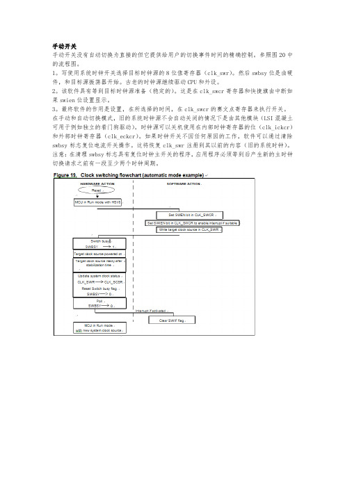
手动开关手动开关没有自动切换为直接的但它提供给用户的切换事件时间的精确控制。
参照图20中的流程图。
1。
写使用系统时钟开关选择目标时钟源的8位值寄存器(clk_swr)。
然后swbsy位是由硬件,和目标源振荡器开始。
古老的时钟源继续驱动CPU和外设。
2。
该软件具有等到目标时钟源准备(稳定的)。
这是在clk_swcr寄存器和快捷旗由中断如果swien位设置显示。
3。
最终软件的作用是设置,在所选择的时间,在clk_swcr的赛文点寄存器来执行开关。
在手动和自动切换模式,旧的系统时钟源不会自动关闭的情况下是由其他模块(LSI混凝土可用于例如独立的看门狗驱动)。
时钟源可以关机使用在内部时钟寄存器的位(clk_ickcr)和外部时钟寄存器(clk_eckcr)。
如果时钟开关不因任何原因的工作,软件可以通过清除swbsy标志复位电流开关操作。
这将恢复clk_swr注册到其以前的内容(旧的系统时钟)。
注意:在清理swbsy标志具有复位时钟主开关的程序,应用程序必须等到后产生新的主时钟切换请求之前有一段至少两个时钟周期。
9.7周门控时钟(PCG)外周时钟门控(PCG)模式选择性地启用或禁用系统时钟(SYSCLK)连接到外围设备在运行或慢速模式的任何时间来优化功耗。
设备复位后,所有的外设时钟被禁用。
唯一的一点是在复位状态是默认启用pcken27因为它用于启动。
软件已被正确地写入关掉ROM Bootloader执行后的时钟。
您可以启用时钟的任何外围设置在clk_pckenrx周围门控时钟寄存器的相应pcken点。
●使周围,首先使在clk_pckenr相应的pcken点寄存器然后设置使点周围的外围控制寄存器。
●禁用适当的外围,先禁用在周边的适当位控制寄存器,然后停止相应的时钟。
注:蜂鸣器,RTC和液晶显示器是由不同的SYSCLK特定的时钟,使他们继续运行,即使时钟门控的外设寄存器是断言。
9.8时钟安全系统(CSS)9.8.1时钟安全系统对HSE时钟安全系统(CSS)监控HSE晶体时钟源故障时安全作为系统时钟。
Silicon Labs EFM8UB2 Errata文件说明书
EFM8 Universal Bee FamilyEFM8UB2 ErrataThis document contains information on the errata of revision A of EFM8UB2.For errata on older revisions, please refer to the errata history for the device. The device data sheet explains how to identify chip revision, either from package marking or electronically.Errata effective date: August 22, 2016.Errata Summary 1. Errata SummaryTable 1.1. Errata Status Summary2. Detailed Errata Descriptions2.1 BL_E102 – USB Bootloader Not AvailableThis issue will be resolved in revision B devices.More information on the bootloader can be found in the device data sheet and in AN945: EFM8 Factory Bootloader User Guide. Appli-cation notes can be found on the Silicon Labs website (/8bit-appnotes) and in Simplicity Studio under [Application Notes].Revision History 3. Revision History3.1 Revision 0.4August 22, 2016BL_E102: Updated fixed revision to B. The previous version of this errata stated the bootloader was available on revision A devices with a date code of 1544 or later. This is incorrect. The bootloader is available in revision B devices.3.2 Revision 0.3November 24, 2015Updated Errata #1 (USB Bootloader Not Available)•Added designator BL_E102.•Updated fixed revision to A, date code 1544 and later.3.3 Revision 0.2June 10, 2015Updated Errata #1 (USB Bootloader Not Available)•Updated description to reference data sheet revision 1.2.•Updated affected condition with expected behavior.•Updated workaround with warning to not write 0xA5 to Bootloader Signature Byte.3.4 Revision 0.1January 30, 2015Initial release.Silicon Laboratories Inc.400 West Cesar Chavez Austin, TX 78701USASimplicity StudioOne-click access to MCU and wireless tools, documentation, software, source code libraries & more. Available for Windows, Mac and Linux!IoT Portfolio /IoTSW/HW/simplicityQuality /qualitySupport and CommunityDisclaimerSilicon Labs intends to provide customers with the latest, accurate, and in-depth documentation of all peripherals and modules available for system and software implementers using or intending to use the Silicon Labs products. Characterization data, available modules and peripherals, memory sizes and memory addresses refer to each specific device, and "Typical" parameters provided can and do vary in different applications. Application examples described herein are for illustrative purposes only. Silicon Labs reserves the right to make changes without further notice and limitation to product information, specifications, and descriptions herein, and does not give warranties as to the accuracy or completeness of the included information. Silicon Labs shall have no liability for the consequences of use of the information supplied herein. This document does not imply or express copyright licenses granted hereunder to design or fabricate any integrated circuits. The products are not designed or authorized to be used within any Life Support System without the specific written consent of Silicon Labs. A "Life Support System" is any product or system intended to support or sustain life and/or health, which, if it fails, can be reasonably expected to result in significant personal injury or death. Silicon Labs products are not designed or authorized for military applications. Silicon Labs products shall under no circumstances be used in weapons of mass destruction including (but not limited to) nuclear, biological or chemical weapons, or missiles capable of delivering such weapons.Trademark InformationSilicon Laboratories Inc.® , Silicon Laboratories®, Silicon Labs®, SiLabs® and the Silicon Labs logo®, Bluegiga®, Bluegiga Logo®, Clockbuilder®, CMEMS®, DSPLL®, EFM®, EFM32®, EFR, Ember®, Energy Micro, Energy Micro logo and combinations thereof, "the world’s most energy friendly microcontrollers", Ember®, EZLink®, EZRadio®, EZRadioPRO®, Gecko®, ISOmodem®, Precision32®, ProSLIC®, Simplicity Studio®, SiPHY®, Telegesis, the Telegesis Logo®, USBXpress® and others are trademarks or registered trademarks of Silicon Labs. ARM, CORTEX, Cortex-M3 and THUMB are trademarks or registered trademarks of ARM Holdings. Keil is a registered trademark of ARM Limited. All other products or brand names mentioned herein are trademarks of their respective holders.。
- 1、下载文档前请自行甄别文档内容的完整性,平台不提供额外的编辑、内容补充、找答案等附加服务。
- 2、"仅部分预览"的文档,不可在线预览部分如存在完整性等问题,可反馈申请退款(可完整预览的文档不适用该条件!)。
- 3、如文档侵犯您的权益,请联系客服反馈,我们会尽快为您处理(人工客服工作时间:9:00-18:30)。
AN945:EFM8 Factory Bootloader用户指南本文档介绍了工厂编程的引导加载程序可用于EFM8设备。
除了描述引导程序的功能,本文档还详细介绍了如何使用引导加载程序并更新Bootloader固件源代码或python主机软件,如果需要定制。
关键点EFM8工厂编程的引导加载程序提供基本的生产编程或现场更新支持。
•主机端都提供源代码python工具和bootloader 件来启用自定义。
1介绍EFM8设备在工厂中使用引导加载程序进行编程。
此引导程序启用:1. 生产编程- 可以在生产环境中对设备进行编程,而无需使用调试接口需要PCB上的接入点和调试适配器。
2. 2.现场更新- 可以在现场的设备上发布更新,无需最终用户访问调试引脚或使用调试适配器硬件。
引导加载程序主要用于具有最小功能集的生产编程,但也可用于现场更新。
因为几个EFM8变体可以有2 KB的闪存,引导程序的设计尽可能小。
例如,UART和SMBus版本消耗单个512闪存页面,USB版本消耗1.5 KB闪存。
另外,bootloader通常位于代码安全页面中,以使引导程序能够写入和擦除锁定的应用程序空间。
更多信息在每个设备上的引导加载程序放置位置可以在设备数据手册或参考手册中找到。
22. USB或UART引导加载程序入门这些步骤假定使用入门套件。
使用自定义硬件时,步骤相同。
这些步骤还假设应用笔记zip文件已经下载到PC,或者使用Simplicity访问文件工作室。
应用程序zip文件可以在Silicon Labs网站(/8bit-appnotes)上找到。
•将Bootloader下载到设备如果引导加载程序尚未在设备上,请使用Simplicity Studio将Bootloader下载到设备,并按以下步骤操作。
日期代码在设备勘误表中列出的日期之后的顶部标记的设备可以支持引导加载程序并可能具有bootloader预装。
在此之前的日期代码的设备将不能与引导程序一起使用。
•打开Simplicity Studio。
•将入门工具包连接到PC。
•将套件开关移动到[AEM]位置。
•单击Simplicity Studio左窗格中的[Refresh detected hardware]按钮。
该套件应显示在[Detected Hardware]区。
•单击工具包,然后单击Simplicity Studio的[tool]区域中的[Flash Programmer]图块。
•单击[Erase]按钮。
•单击[Browse]按钮,导航到套件设备的预编译引导加载程序十六进制文件,单击[Open],然后单击[Program]。
使用引导加载程序将应用程序下载到设备•由于闪存最初为空(从上一步中的擦除命令开始),器件将在引导加载模式下自动启动。
•对于USB引导加载设备(即EFM8UB1),请将第二条USB电缆连接到设备USB接口的底部边缘入门套件•在与Windows中的efm8load Python主机工具([Start]> [Run]> [command]相同的目录中打开命令行窗口)。
•键入efm8load.exe,后跟Bootload记录的名称。
例如:efm8load.exe EFM8UB1_RainbowBlinky.efm8这将将文件下载到入门工具包并自动运行应用程序。
注意:请注意,bootload记录是由hex2boot.exe主机端工具创建的。
有关此工具的更多信息,请参见5.使用主机端工具。
3. 启动SMBus引导加载程序这些步骤假定使用入门套件。
使用自定义硬件时,步骤相同。
这些步骤还假设应用笔记zip文件已经下载到PC,或者使用Simplicity访问文件工作室。
应用程序zip文件可以在Silicon Labs网站(/8bit-appnotes)上找到。
由于SMBus不是作为PC上端口的总线类型,因此这些步骤使用CP2112 USB to SMBus评估板示范目的。
•将EFM8LB1 STK连接到CP2112 EK。
•在EFM8LB1 STK和CP2112 EK之间安装三条跳线,以连接SDA,SCK和GND信号。
使用下表作为指导。
请注意,EFM8LB1 STK的SMBus引导加载程序使用SDA和SCK的非标准引脚分配以适应STK设计。
另外,请确保在CP2112 EK的J7引脚1:2上安装跳线以启用SMBus上拉电阻器。
•使用USB电缆将两个电路板连接到PC。
•将Bootloader下载到设备如果SMBus引导加载程序尚未在设备上,请使用Simplicity Studio将引导加载程序下载到设备,步骤如下下面。
注意:请注意,用于STK的SMBus引导加载程序的引脚分配与预加载的标准SMBus引导加载程序不同EFM8LB1设备。
•开放简约工作室。
•将入门工具包连接到PC。
•将套件开关移动到[AEM]位置。
•单击Simplicity Studio左窗格中的[刷新检测到的硬件]按钮。
该套件应显示在[检测硬件]区。
•单击工具包,然后单击Simplicity Studio的[工具]区域中的[Flash程序员]图块。
•单击[擦除]按钮。
•单击[浏览]按钮,导航到套件设备(EFM8LB12F64E_QFN32)的预编译引导加载程序十六进制文件,单击[打开],然后单击[程序]。
•使用引导加载程序将应用程序下载到设备•由于闪存最初为空(从上一步中的擦除命令开始),器件将在引导加载模式下自动启动。
•在与Windows中的efm8load Python主机工具([Start]> [Run]> [command]相同的目录中打开命令行窗口)。
•键入efm8load.exe,后跟SMBus引导加载程序开关和引导加载记录的名称。
例如:efm8load.exe -psmb EFM8LB1_RainbowBlinky.efm8这将通过CP2112 EK将文件下载到入门工具包。
efm8load实用程序使用默认的100 kHz时钟速率。
使用[-baud]开关调节时钟频率。
使用RainbowBlinky应用程序在STK上运行时,按[PB0]按钮启动引导程序。
RainbowBlinky预制引导映像位于:。
\ AN945SW_SMB \ Firmware \ EFM8LB1_SLSTK2030A \ RainbowBlinky \ BIN \ EFM8LB1_RainbowBlinky.efm8。
注意:请注意,bootload记录是由hex2boot.exe主机端工具创建的。
有关此工具的更多信息,请参见5.使用主机端工具。
4.功能概述4.1系统架构如下图所示,EFM8引导加载程序工具将读取一个映像文件(十六进制或二进制),并将其转换为一系列引导程序2命令。
这些命令格式化为引导记录,存储在文件中或直接发送到EFM8设备。
使用相同的二进制记录格式,无论是保存到文件还是通过引导加载程序传输。
引导程序命令被设计为不返回任何数据,并且它们包含执行命令所需的所有信息并确定成功或失败。
要实现嵌入式主机,请从文件读取每个记录,将其发送到EFM8设备,并等待确认。
因为引导记录文件是二进制的,所以它对图像增加了很少的开销,应该很容易嵌入。
4.2引导程序概述所有设备都使用UART(〜500字节),SMBus(〜500字节)或USB HID(〜1.5 kB)引导加载程序进行预编程。
这个引导程序驻留在代码安全页面中。
如果它太大,不适合代码安全页面,它也将占用最后一页代码闪存。
它可以擦除如果不需要。
锁定字节之前的字节是Bootloader签名字节。
将此字节设置为值0xA5表示引导加载程序的存在在系统中。
此位置中的任何其他值表示引导加载程序不存在于闪存中。
当存在引导加载程序时,设备将在任何重置后跳转到引导加载程序向量,从而允许引导程序运行。
引导程序然后确定设备是否应保持在引导加载模式或跳转到位于0x0000的复位向量。
当bootloader不存在,任何复位后,器件将跳转到0x0000的复位向量。
4.3引导加载程序功能特性本节讨论引导程序固件的特定功能。
请注意,引导加载程序源代码和预构建的十六进制文件可在Simplicity Studio中使用[Software Examples]图块或可用在Silicon Labs网站(https:///8bit-appnotes)上。
这使Bootloader可以在任何设备上进行重新编程如果意外删除,并且可以根据需要为任何应用程序定制引导程序。
AN945:EFM8 Factory Bootloader用户指南功能概述SILABS。
4.3.1进入引导加载模式•在任何复位时,如果闪存地址0x0000为0xFF(即,未编程复位向量的第一个字节),引导加载程序将启动。
这个确保新的或已擦除的部件启动引导程序进行生产编程。
为了强壮,Bootloader将首先擦除Flash页面0,最后写入闪存地址0x0000。
这样可以确保任何中断引导加载操作将在中断擦除结束重新启动。
•要根据需要启动引导加载程序,应用程序固件可以在Bank 0(数据地址0x00)的R0中设置签名值0xA5,然后启动设备的软件复位。
如果引导加载程序使用R0中的签名值看到软件复位,则它将启动引导程序执行而不是跳转到应用程序。
•为了在应用程序损坏的情况下提供故障安全操作,引导加载程序将在上电复位(POR)或引脚复位时启动如果引脚保持低电平超过50μs。
表4.1总结中提供了每个设备和包的入口引脚的完整列表引导加载模式条目的引脚第10页。
此引导加载程序输入法的引脚也可以通过查看efm8_device.h文件中的bootloader源代码。
没有选项禁用此条目方法。
4.3.1.1Rainbow Blinky示例[Demo]文件夹中的[Rainbow Blinky](或EFM8SB1的[PWM Blinky])示例可以使用[Software Examples] Simplicity Studio演示如何使用软件重置条目方法创建可以进入引导加载模式的应用程序。
除了标准的Rainbow Blinky操作之外,本应用程序还查看入门工具包上的PB0是否被按下。
如果是,那么示例在LCD屏幕上显示[Loader],将0xA5的签名值写入R0地址(数据地址0x00),并启动软件重置。
当这种情况发生时,引导加载程序会看到数据地址的签名值,并保持在引导加载模式。
该这样做的代码很简单,如下所示:// Start the bootloader if PB0 is pressedif (BSP_PB0 == BSP_PB_PRESSED){// Print "Loader" to the screencolorIndex = 8;DrawColorName();// Write R0 and issue a software reset*((uint8_t SI_SEG_DATA *)0x00) = 0xA5;RSTSRC = RSTSRC_SWRSF__SET | RSTSRC_PORSF__SET;}4.3.2通讯接口•引导加载程序通信接口被轮询,因为引导加载程序无法访问第0页的中断向量。