caputer生成网表报错原因解析#(精选.)
caputer生成网表报错原因解析演示教学
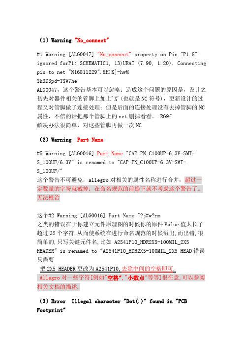
c a p u t e r生成网表报错原因解析(1)Warning "No_connect"#1 Warning [ALG0047] "No_connect" property on Pin "P1.8" ignored forP1: SCHEMATIC1, 13)URAT (7.90, 1.20). Connecting pin to net "N16811229".&H)K]-hwM$k3D3pd-T$W7heALG0047,这个警告基本可以忽略;造成这个问题的原因是,设计之初先对器件相关的管脚上加上'X'(也就是NC符号),更新设计的过程又对管脚做了连接处理;但是后面的连接处理没有去掉管脚的NC 属性,不信的话把那个管脚上的net删掉看看。
RG9f解决办法很简单,对这些管脚再做一次NC(2)Warning Part Name#5 Warning [ALG0016] Part Name "CAP PN_C100UP-6.3V-SMT-S_100UF/6.3V" is renamed to "CAP PN_C100UP-6.3V-SMT-S_100UF/"这个警告不可避免,allegro对相关的属性名称进行合并,超过一定数量的字符就截掉;在命名规范的前提下就不考虑这个警告了。
无法根治这个#2 Warning [ALG0016] Part Name "?j#w?rm之类的错误在于你建立元件原理图的时候你的原件Value值太长了超过32个字符,从而使系统在进行命名规范的时候溢出,而出错,很简单的,只写关键元件名,比如 A2541P10_HDR2X5-100MIL_2X5 HEADER" is renamed to "A2541P10_HDR2X5-100MIL_2X5 HEAD错误只需要把2X5 HEADER更改为A2541P10,去除中间的空格即可.Allegro对一些字符[例如"空格","小数点"等等]很在意,可以参阅相关文档的描述.(3)Error Illegal character "Dot(.)" found in "PCB Footprint"#1 Error [ALG0081] Illegal character "Dot(.)" found in "PCB Footprint" property for component instance C255:PG16_AC97, PG16_AC97 (226.06, 132.08) .封装命名不能包含“.”(4)Error Illegal character "Forward Slash(/)" found in "PCB Footprint" property#1 Error [ALG0081] Illegal character "Forward Slash(/)" found in "PCB Footprint" property for component instanceC255: PG16_AC97, PG16_AC97 (226.06, 132.08) .#2 Error [ALG0081] Illegal character "Forward Slash(/)" found in "PCB Footprint" property for component instance D3: PG01_LED&Switch&7-Segment Disp, PG01_LED&Switch&7-Segment Disp (93.98, 33.02) .#3 Error [ALG0081] Illegal character "Forward Slash(/)" found in "PCB Footprint" property for component instanceC245: PG16_AC97, PG16_AC97 (205.74, 35.56) .封装命名不能包含“/”(5)比较隐藏的排除法Loading... E:\FPGA\SCH\allegro/pstchip.dat#34 WARNING(SPCODD-34): Expected ';' character on line 5308. Check the name and value syntax for invalid characters in theprimitive definition before the line number.ERROR(SPCODD-47): File ./allegro/pstchip.dat could not be loaded, and the packaging operation did notcomplete. Check the pxl.log file for the errors causingthis situation and package the design again.#53 ERROR(SPCODD-53): Packaging cannot be completed because packaging has encountered a null object ID. The design may not have been saved correctly. Save the schematic and rerun packaging.#187 Error [ALG0036] Unable to read logical netlist data.Exiting... "D:\Cadence\SPB_16.2\tools\capture\pstswp.exe" -pst -d "E:\FPGA\SCH\motherboard.dsn" -n"E:\FPGA\SCH\allegro" -c"D:\Cadence\SPB_16.2\tools\capture\allegro.cfg" -v 3 -j "PCB Footprint"*** Done*******掌握排错方法,查找文件pstchip.dat,第on line 5308 看看错误,便可以解决(6)封装命名中不能包含“小数点”、“/”、“空格”,把空格换成下划线或删除,可以解决*********************************************************** *********************** Netlisting the design*********************************************************** **********************Design Name:E:\FPGA\SCH\basicboard.dsnNetlist Directory:E:\FPGA\SCH\allegroConfiguration File:D:\Cadence\SPB_16.2\tools\capture\allegro.cfgSpawning... "D:\Cadence\SPB_16.2\tools\capture\pstswp.exe" -pst -d "E:\FPGA\SCH\basicboard.dsn" -n"E:\FPGA\SCH\allegro" -c"D:\Cadence\SPB_16.2\tools\capture\allegro.cfg" -v 3 -j "PCB Footprint"#1 Error [ALG0081] Illegal character "White space" found in "PCB Footprint" property for component instance MG2: Basic, PG06_Stepmotor (180.34, 83.82) .#2 Error [ALG0081] Illegal character "White space" found in "PCB Footprint" property for component instance ISO1: Basic, PG05_DC Motor (134.62, 40.64) .#3 Info: PCB Editor does not support Dots(.), Forward Slash(/) and White space in footprint names. The supported characters include Alphabets, Numerics, Underscore(_) and Hyphen(-).#4 Aborting Netlisting... Please correct the above errors and retry.Exiting... "D:\Cadence\SPB_16.2\tools\capture\pstswp.exe" -pst -d "E:\FPGA\SCH\basicboard.dsn" -n"E:\FPGA\SCH\allegro" -c"D:\Cadence\SPB_16.2\tools\capture\allegro.cfg" -v 3 -j "PCB Footprint"*** Done ***封装命名中不能包含“小数点”、“/”、“空格”,把空格换成下划线或删除,可以解决(7)Warning#11 Warning [ALG0051] Pin "GND" is renamed to "GND#A6" after substituting illegal characters in Package XC3S1400A-4FG676-C_0FF , U1A: SCHEMATIC1, PG01_FPGACONFIG (2.40,3.10).#12 Warning [ALG0051] Pin "GND" is renamed to "GND#A11" after substituting illegal characters in Package XC3S1400A-4FG676-C_0FF , U1A: SCHEMATIC1, PG01_FPGACONFIG (2.40,3.10).#13 Warning [ALG0051] Pin "GND" is renamed to "GND#A1" after substituting illegal characters in Package XC3S1400A-4FG676-C_0FF , U1A: SCHEMATIC1, PG01_FPGACONFIG (2.40,3.10).#14 Warning [ALG0051] Pin "GND" is renamed to "GND#W8" after substituting illegal characters in Package XC3S1400A-4FG676-C_0FF , U1A: SCHEMATIC1, PG01_FPGACONFIG (2.40,3.10).这条警告信息,在命名规范的前提下就不考虑这个警告了。
Cadence中Capture向Allegro中导入网表时的常见错误

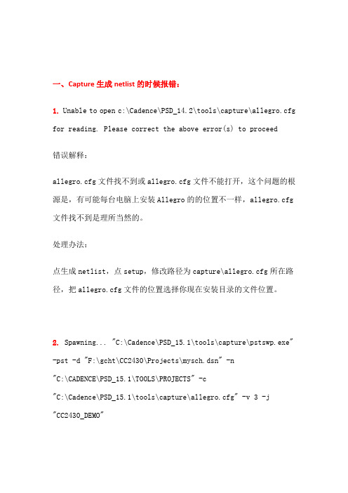
一、Capture生成netlist的时候报错:1.Unable to open c:\Cadence\PSD_14.2\tools\capture\allegro.cfg for reading. Please correct the above error(s) to proceed错误解释:allegro.cfg文件找不到或allegro.cfg文件不能打开,这个问题的根源是,有可能每台电脑上安装Allegro的的位置不一样,allegro.cfg 文件找不到是理所当然的。
处理办法:点生成netlist,点setup,修改路径为capture\allegro.cfg所在路径,把allegro.cfg文件的位置选择你现在安装目录的文件位置。
2. Spawning... "C:\Cadence\PSD_15.1\tools\capture\pstswp.exe" -pst -d "F:\gcht\CC2430\Projects\mysch.dsn" -n"C:\CADENCE\PSD_15.1\TOOLS\PROJECTS" -c"C:\Cadence\PSD_15.1\tools\capture\allegro.cfg" -v 3 -j"CC2430_DEMO"#1 Error [ALG0012] Property "PCB Footprint" missing from instance U3: SCHEMATIC1, PAGE1 (2.00, 2.10).#2 Error [ALG0012] Property "PCB Footprint" missing from instance C2: SCHEMATIC1, PAGE1 (2.30, 0.30).#17 Aborting Netlisting... Please correct the above errors and retry.错误解释:Error [ALG0012] Property "PCB Footprint" missing from part <Part Reference>: <Schematic> , <Page> (<LocationX> , <LocationY)>A PCB Footprint (JEDEC_TYPE in Allegro) is required for all parts in Allegro. Therefore all parts without this property are listed before aborting the netlisting. You can add the PCB Footprint property by selecting the part listed, then choosing Edit Properties from the pop-up menu and placing a value, such as dip14_3, on the part.在Allegro中,每个器件都需要一个PCB封装。
Cadence中Capture向Allegro中导入网表时的常见错误
一、Capture生成netlist的时候报错:1.Unable to open c:\Cadence\PSD_14.2\tools\capture\allegro.cfg for reading. Please correct the above error(s) to proceed错误解释:allegro.cfg文件找不到或allegro.cfg文件不能打开,这个问题的根源是,有可能每台电脑上安装Allegro的的位置不一样,allegro.cfg 文件找不到是理所当然的。
处理办法:点生成netlist,点setup,修改路径为capture\allegro.cfg所在路径,把allegro.cfg文件的位置选择你现在安装目录的文件位置。
2. Spawning... "C:\Cadence\PSD_15.1\tools\capture\pstswp.exe" -pst -d "F:\gcht\CC2430\Projects\mysch.dsn" -n"C:\CADENCE\PSD_15.1\TOOLS\PROJECTS" -c"C:\Cadence\PSD_15.1\tools\capture\allegro.cfg" -v 3 -j"CC2430_DEMO"#1 Error [ALG0012] Property "PCB Footprint" missing from instance U3: SCHEMATIC1, PAGE1 (2.00, 2.10).#2 Error [ALG0012] Property "PCB Footprint" missing from instance C2: SCHEMATIC1, PAGE1 (2.30, 0.30).#17 Aborting Netlisting... Please correct the above errors and retry.错误解释:Error [ALG0012] Property "PCB Footprint" missing from part <Part Reference>: <Schematic> , <Page> (<LocationX> , <LocationY)>A PCB Footprint (JEDEC_TYPE in Allegro) is required for all parts in Allegro. Therefore all parts without this property are listed before aborting the netlisting. You can add the PCB Footprint property by selecting the part listed, then choosing Edit Properties from the pop-up menu and placing a value, such as dip14_3, on the part.在Allegro中,每个器件都需要一个PCB封装。
【免费下载】cadence生成网络表时出现如下错误解决办法
U(ZE0B5L5b%X;n4g Allegro对一些字符[例如"空格","小数点"等等]很在意,可以参阅相关文档的描述.(3)Error Illegal character "Dot(.)" found in "PCB Footprint"#1 Error [ALG0081] Illegal character "Dot(.)" found in "PCB Footprint" property for componen t instance C255: PG16_AC97, PG16_AC97 (226.06, 132.08) .封装命名不能包含“.”(4)Error Illegal character "Forward Slash(/)" found in "PCB Footprint" property#1 Error [ALG0081] Illegal character "Forward Slash(/)" found in "PCB Footprint" property for component instance C255: PG16_AC97, PG16_AC97 (226.06, 132.08) .#2 Error [ALG0081] Illegal character "Forward Slash(/)" found in "PCB Footprint" property for component instance D3: PG01_LED&Switch&7-Segment Disp, PG01_LED&Switch&7-Segment Disp (93.98, 33.02) .#3 Error [ALG0081] Illegal character "Forward Slash(/)" found in "PCB Footprint" property for component instance C245: PG16_AC97, PG16_AC97 (205.74, 35.56) .封装命名不能包含“/”(5)比较隐藏的排除法Loading... E:\FPGA\SCH\allegro/pstchip.dat#34 WARNING(SPCODD-34): Expected ';' character on line 5308.Check the name and value syntax for invalid characters in theprimitive definition before the line number.ERROR(SPCODD-47): File ./allegro/pstchip.dat could not be loaded, and the pac kaging operation did not complete. Check the pxl.log file for the errors causing this situ ation and package the design again.#53 ERROR(SPCODD-53): Packaging cannot be completed because packaging has enc ountered a null object ID. The design may not have been saved correctly. Save the sc hematic and rerun packaging.#187 Error [ALG0036] Unable to read logical netlist data.Exiting... "D:\Cadence\SPB_16.2\tools\capture\pstswp.exe" -pst -d "E:\FPGA\SCH\motherb oard.dsn" -n "E:\FPGA\SCH\allegro" -c "D:\Cadence\SPB_16.2\tools\capture\allegro.cfg" -v 3 -j "PCB Footprint"*** Done*******掌握排错方法,查找文件pstchip.dat,第on line 5308 看看错误,便可以解决(6)封装命名中不能包含“小数点”、“/”、“空格”,把空格换成下划线或删除,可以解决********************************************************************************** Netlisting the design*********************************************************************************Design Name:E:\FPGA\SCH\basicboard.dsnNetlist Directory:E:\FPGA\SCH\allegroConfiguration File:D:\Cadence\SPB_16.2\tools\capture\allegro.cfgSpawning... "D:\Cadence\SPB_16.2\tools\capture\pstswp.exe" -pst -d "E:\FPGA\SCH\basic board.dsn" -n "E:\FPGA\SCH\allegro" -c "D:\Cadence\SPB_16.2\tools\capture\allegro.cfg" -v 3 -j "PCB Footprint"#1 Error [ALG0081] Illegal character "White space" found in "PCB Footprint" property f or component instance MG2: Basic, PG06_Stepmotor (180.34, 83.82) .#2 Error [ALG0081] Illegal character "White space" found in "PCB Footprint" property f or component instance ISO1: Basic, PG05_DC Motor (134.62, 40.64) .#3 Info: PCB Editor does not support Dots(.), Forward Slash(/) and White space in foot print names. The supported characters include Alphabets, Numerics, Underscore(_) and Hyphen(-).#4 Aborting Netlisting... Please correct the above errors and retry.Exiting... "D:\Cadence\SPB_16.2\tools\capture\pstswp.exe" -pst -d "E:\FPGA\SCH\basicboa rd.dsn" -n "E:\FPGA\SCH\allegro" -c "D:\Cadence\SPB_16.2\tools\capture\allegro.cfg" -v 3 -j "PCB Footprint"*** Done ***封装命名中不能包含“小数点”、“/”、“空格”,把空格换成下划线或删除,可以解决(7)Warning#11 Warning [ALG0051] Pin "GND" is renamed to "GND#A6" after substituting illegal ch aracters in Package XC3S1400A-4FG676-C_0FF , U1A: SCHEMATIC1, PG01_FPGACO NFIG (2.40, 3.10).#12 Warning [ALG0051] Pin "GND" is renamed to "GND#A11" after substituting illegal c haracters in Package XC3S1400A-4FG676-C_0FF , U1A: SCHEMATIC1, PG01_FPGAC ONFIG (2.40, 3.10).#13 Warning [ALG0051] Pin "GND" is renamed to "GND#A1" after substituting illegal ch aracters in Package XC3S1400A-4FG676-C_0FF , U1A: SCHEMATIC1, PG01_FPGACO NFIG (2.40, 3.10).#14 Warning [ALG0051] Pin "GND" is renamed to "GND#W8" after substituting illegal c haracters in Package XC3S1400A-4FG676-C_0FF , U1A: SCHEMATIC1, PG01_FPGAC ONFIG (2.40, 3.10).这条警告信息,在命名规范的前提下就不考虑这个警告了。
ORCAD出ALLEGRO网表非法错误案例:
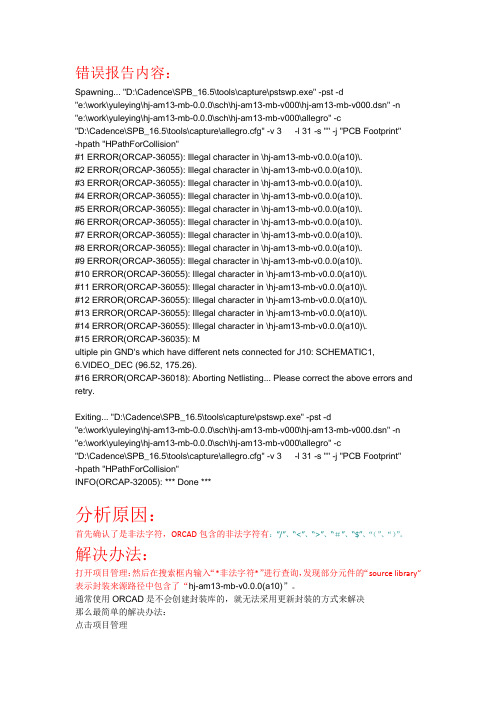
错误报告内容:Spawning... "D:\Cadence\SPB_16.5\tools\capture\pstswp.exe" -pst -d"e:\work\yuleying\hj-am13-mb-0.0.0\sch\hj-am13-mb-v000\hj-am13-mb-v000.dsn" -n "e:\work\yuleying\hj-am13-mb-0.0.0\sch\hj-am13-mb-v000\allegro" -c"D:\Cadence\SPB_16.5\tools\capture\allegro.cfg" -v 3 -l 31 -s "" -j "PCB Footprint"-hpath "HPathForCollision"#1 ERROR(ORCAP-36055): Illegal character in \hj-am13-mb-v0.0.0(a10)\.#2 ERROR(ORCAP-36055): Illegal character in \hj-am13-mb-v0.0.0(a10)\.#3 ERROR(ORCAP-36055): Illegal character in \hj-am13-mb-v0.0.0(a10)\.#4 ERROR(ORCAP-36055): Illegal character in \hj-am13-mb-v0.0.0(a10)\.#5 ERROR(ORCAP-36055): Illegal character in \hj-am13-mb-v0.0.0(a10)\.#6 ERROR(ORCAP-36055): Illegal character in \hj-am13-mb-v0.0.0(a10)\.#7 ERROR(ORCAP-36055): Illegal character in \hj-am13-mb-v0.0.0(a10)\.#8 ERROR(ORCAP-36055): Illegal character in \hj-am13-mb-v0.0.0(a10)\.#9 ERROR(ORCAP-36055): Illegal character in \hj-am13-mb-v0.0.0(a10)\.#10 ERROR(ORCAP-36055): Illegal character in \hj-am13-mb-v0.0.0(a10)\.#11 ERROR(ORCAP-36055): Illegal character in \hj-am13-mb-v0.0.0(a10)\.#12 ERROR(ORCAP-36055): Illegal character in \hj-am13-mb-v0.0.0(a10)\.#13 ERROR(ORCAP-36055): Illegal character in \hj-am13-mb-v0.0.0(a10)\.#14 ERROR(ORCAP-36055): Illegal character in \hj-am13-mb-v0.0.0(a10)\.#15 ERROR(ORCAP-36035): Multiple pin GND's which have different nets connected for J10: SCHEMATIC1,6.VIDEO_DEC (96.52, 175.26).#16 ERROR(ORCAP-36018): Aborting Netlisting... Please correct the above errors and retry.Exiting... "D:\Cadence\SPB_16.5\tools\capture\pstswp.exe" -pst -d"e:\work\yuleying\hj-am13-mb-0.0.0\sch\hj-am13-mb-v000\hj-am13-mb-v000.dsn" -n "e:\work\yuleying\hj-am13-mb-0.0.0\sch\hj-am13-mb-v000\allegro" -c"D:\Cadence\SPB_16.5\tools\capture\allegro.cfg" -v 3 -l 31 -s "" -j "PCB Footprint"-hpath "HPathForCollision"INFO(ORCAP-32005): *** Done ***分析原因:首先确认了是非法字符,ORCAD包含的非法字符有:”/”、“<”、“>”、“#”、“$”、“(”、“)”。
caputer生成网表报错原因解析
(1)Warning "No_connect"#1 Warning [ALG0047] "No_connect" property on Pin "P1.8" ignored forP1: SCHEMATIC1, 13)URAT (7.90, 1.20). Connecting pin to net "N16811229".&H)K]-hwM$k3D3pd-T$W7heALG0047,这个警告基本可以忽略;造成这个问题的原因是,设计之初先对器件相关的管脚上加上'X'(也就是NC符号),更新设计的过程又对管脚做了连接处理;但是后面的连接处理没有去掉管脚的NC 属性,不信的话把那个管脚上的net删掉看看。
RG9f解决办法很简单,对这些管脚再做一次NC(2)Warning Part Name#5 Warning [ALG0016] Part Name "CAP PN_C100UP-6.3V-SMT-S_100UF/6.3V" is renamed to "CAP PN_C100UP-6.3V-SMT-S_100UF/"这个警告不可避免,allegro对相关的属性名称进行合并,超过一定数量的字符就截掉;在命名规范的前提下就不考虑这个警告了。
无法根治这个#2 Warning [ALG0016] Part Name "?j#w?rm之类的错误在于你建立元件原理图的时候你的原件Value值太长了超过32个字符,从而使系统在进行命名规范的时候溢出,而出错,很简单的,只写关键元件名,比如 A2541P10_HDR2X5-100MIL_2X5 HEADER" is renamed to "A2541P10_HDR2X5-100MIL_2X5 HEAD错误只需要把2X5 HEADER更改为A2541P10,去除中间的空格即可.Allegro对一些字符[例如"空格","小数点"等等]很在意,可以参阅相关文档的描述.(3)Error Illegal character "Dot(.)" found in "PCB Footprint"#1 Error [ALG0081] Illegal character "Dot(.)" found in "PCB Footprint" property for component instance C255:PG16_AC97, PG16_AC97 (226.06, 132.08) .封装命名不能包含“.”(4)Error Illegal character "Forward Slash(/)" found in "PCB Footprint" property#1 Error [ALG0081] Illegal character "Forward Slash(/)" found in "PCB Footprint" property for component instanceC255: PG16_AC97, PG16_AC97 (226.06, 132.08) .#2 Error [ALG0081] Illegal character "Forward Slash(/)" found in "PCB Footprint" property for component instance D3: PG01_LED&Switch&7-Segment Disp, PG01_LED&Switch&7-Segment Disp (93.98, 33.02) .#3 Error [ALG0081] Illegal character "Forward Slash(/)" found in "PCB Footprint" property for component instanceC245: PG16_AC97, PG16_AC97 (205.74, 35.56) .封装命名不能包含“/”(5)比较隐藏的排除法Loading... E:\FPGA\SCH\allegro/pstchip.dat#34 WARNING(SPCODD-34): Expected ';' character on line 5308. Check the name and value syntax for invalid characters intheprimitive definition before the line number.ERROR(SPCODD-47): File ./allegro/pstchip.dat could not be loaded, and the packaging operation did not complete. Check the pxl.log file for the errors causingthis situation and package the design again.#53 ERROR(SPCODD-53): Packaging cannot be completed because packaging has encountered a null object ID. The design may not have been saved correctly. Save the schematic and rerun packaging.#187 Error [ALG0036] Unable to read logical netlist data.Exiting... "D:\Cadence\SPB_16.2\tools\capture\pstswp.exe" -pst -d "E:\FPGA\SCH\motherboard.dsn" -n"E:\FPGA\SCH\allegro" -c"D:\Cadence\SPB_16.2\tools\capture\allegro.cfg" -v 3 -j "PCB Footprint"*** Done*******掌握排错方法,查找文件pstchip.dat,第on line 5308 看看错误,便可以解决(6)封装命名中不能包含“小数点”、“/”、“空格”,把空格换成下划线或删除,可以解决*********************************************************** *********************** Netlisting the design*********************************************************** **********************Design Name:E:\FPGA\SCH\basicboard.dsnNetlist Directory:E:\FPGA\SCH\allegroConfiguration File:D:\Cadence\SPB_16.2\tools\capture\allegro.cfgSpawning... "D:\Cadence\SPB_16.2\tools\capture\pstswp.exe" -pst -d "E:\FPGA\SCH\basicboard.dsn" -n"E:\FPGA\SCH\allegro" -c"D:\Cadence\SPB_16.2\tools\capture\allegro.cfg" -v 3 -j "PCB Footprint"#1 Error [ALG0081] Illegal character "White space" found in "PCB Footprint" property for component instance MG2: Basic, PG06_Stepmotor (180.34, 83.82) .#2 Error [ALG0081] Illegal character "White space" found in "PCB Footprint" property for component instance ISO1: Basic, PG05_DC Motor (134.62, 40.64) .#3 Info: PCB Editor does not support Dots(.), Forward Slash(/) and White space in footprint names. The supported characters include Alphabets, Numerics, Underscore(_) and Hyphen(-).#4 Aborting Netlisting... Please correct the above errors and retry.Exiting... "D:\Cadence\SPB_16.2\tools\capture\pstswp.exe" -pst -d "E:\FPGA\SCH\basicboard.dsn" -n"E:\FPGA\SCH\allegro" -c"D:\Cadence\SPB_16.2\tools\capture\allegro.cfg" -v 3 -j "PCB Footprint"*** Done ***封装命名中不能包含“小数点”、“/”、“空格”,把空格换成下划线或删除,可以解决(7)Warning#11 Warning [ALG0051] Pin "GND" is renamed to "GND#A6" after substituting illegal characters in Package XC3S1400A-4FG676-C_0FF , U1A: SCHEMATIC1, PG01_FPGACONFIG (2.40,3.10).#12 Warning [ALG0051] Pin "GND" is renamed to "GND#A11" after substituting illegal characters in Package XC3S1400A-4FG676-C_0FF , U1A: SCHEMATIC1, PG01_FPGACONFIG (2.40,3.10).#13 Warning [ALG0051] Pin "GND" is renamed to "GND#A1" after substituting illegal characters in Package XC3S1400A-4FG676-C_0FF , U1A: SCHEMATIC1, PG01_FPGACONFIG (2.40,3.10).#14 Warning [ALG0051] Pin "GND" is renamed to "GND#W8" after substituting illegal characters in Package XC3S1400A-4FG676-C_0FF , U1A: SCHEMATIC1, PG01_FPGACONFIG (2.40,3.10).这条警告信息,在命名规范的前提下就不考虑这个警告了。
Cadence中Capture向Allegro中导入网表时的常见错误讲解学习
一、Capture生成netlist的时候报错:1.Unable to open c:\Cadence\PSD_14.2\tools\capture\allegro.cfg for reading. Please correct the above error(s) to proceed错误解释:allegro.cfg文件找不到或allegro.cfg文件不能打开,这个问题的根源是,有可能每台电脑上安装Allegro的的位置不一样,allegro.cfg 文件找不到是理所当然的。
处理办法:点生成netlist,点setup,修改路径为capture\allegro.cfg所在路径,把allegro.cfg文件的位置选择你现在安装目录的文件位置。
2. Spawning... "C:\Cadence\PSD_15.1\tools\capture\pstswp.exe" -pst -d "F:\gcht\CC2430\Projects\mysch.dsn" -n"C:\CADENCE\PSD_15.1\TOOLS\PROJECTS" -c"C:\Cadence\PSD_15.1\tools\capture\allegro.cfg" -v 3 -j"CC2430_DEMO"#1 Error [ALG0012] Property "PCB Footprint" missing from instance U3: SCHEMATIC1, PAGE1 (2.00, 2.10).#2 Error [ALG0012] Property "PCB Footprint" missing from instance C2: SCHEMATIC1, PAGE1 (2.30, 0.30).#17 Aborting Netlisting... Please correct the above errors and retry.错误解释:Error [ALG0012] Property "PCB Footprint" missing from part <Part Reference>: <Schematic> , <Page> (<LocationX> , <LocationY)>A PCB Footprint (JEDEC_TYPE in Allegro) is required for all parts in Allegro. Therefore all parts without this property are listed before aborting the netlisting. You can add the PCB Footprint property by selecting the part listed, then choosing Edit Properties from the pop-up menu and placing a value, such as dip14_3, on the part.在Allegro中,每个器件都需要一个PCB封装。
candence网标 (orcap-5004)错误解决方法
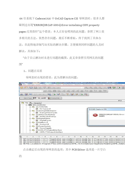
64位系统下Cadence16.6中OrCAD Capture CIS导网表时,很多人都碰到过出现“ERROR(ORCAP-5004):Error initializing COM property pages:无效指针”这个错误,本人正好也喷到的此问题,参照了网上很多相关的方法,依然存在问题,最后不断看帖,终于找到了具体办法,在此特地详细写出实际的解决步骤,方便碰到同样问题的人及时解决,具体如下:“由于自己解决时未进行问题的截图,此文章参照引用网友的问题图”1、问题点还原导网表时出现的错误,此为需解决的问题,点击确定后出现的导网表的选项,其中PCB Editor选项是一片空白的2、解决办法先打开我的电脑C盘,按照此目录“C:\Windows\SysWOW64”找到cmd.exe的应用点击鼠标右键以管理员身份运行进入DOS命令窗口下先复制如下这一行的代码(其中相应文件的路径请按照自己安装的文件路径进行修改)regsvr32 "D:\Program Files(x86)\Cadence\SPB_16.6\tools\capture\orTrueReuse.ocx"在DOS窗口下点击鼠标右键选择粘贴(不能按ctr+v的快捷键)粘贴第一行后如图所示之后直接按回车键,第一个文件更改成功再复制下行的代码(其中相应文件的路径请按照自己安装的文件路径进行修改)regsvr32 "D:\Program Files(x86)\Cadence\SPB_16.6\tools\capture\orpxllite.ocx"继续在DOS窗口下粘贴任然按回车键,第二个文件更改成功此时,两个文件的更改已经成功,我们重新打开Cadence16.6中OrCAD Capture CIS的文件进行查看我们可以看到PCB Editor选项已经正常了,问题完美解决!。
- 1、下载文档前请自行甄别文档内容的完整性,平台不提供额外的编辑、内容补充、找答案等附加服务。
- 2、"仅部分预览"的文档,不可在线预览部分如存在完整性等问题,可反馈申请退款(可完整预览的文档不适用该条件!)。
- 3、如文档侵犯您的权益,请联系客服反馈,我们会尽快为您处理(人工客服工作时间:9:00-18:30)。
(1)Warning "No_connect"#1 Warning [ALG0047] "No_connect" property on Pin "P1.8" ignored forP1: SCHEMATIC1, 13)URAT (7.90, 1.20). Connecting pin to net "N16811229".&H)K]-hwM$k3D3pd-T$W7heALG0047,这个警告基本可以忽略;造成这个问题的原因是,设计之初先对器件相关的管脚上加上'X'(也就是NC符号),更新设计的过程又对管脚做了连接处理;但是后面的连接处理没有去掉管脚的NC 属性,不信的话把那个管脚上的net删掉看看。
RG9f解决办法很简单,对这些管脚再做一次NC(2)Warning Part Name#5 Warning [ALG0016] Part Name "CAP PN_C100UP-6.3V-SMT-S_100UF/6.3V" is renamed to "CAP PN_C100UP-6.3V-SMT-S_100UF/"这个警告不可避免,allegro对相关的属性名称进行合并,超过一定数量的字符就截掉;在命名规范的前提下就不考虑这个警告了。
无法根治这个#2 Warning [ALG0016] Part Name "?j#w?rm之类的错误在于你建立元件原理图的时候你的原件Value值太长了超过32个字符,从而使系统在进行命名规范的时候溢出,而出错,很简单的,只写关键元件名,比如 A2541P10_HDR2X5-100MIL_2X5 HEADER" is renamed to "A2541P10_HDR2X5-100MIL_2X5 HEAD错误只需要把2X5 HEADER更改为A2541P10,去除中间的空格即可.Allegro对一些字符[例如"空格","小数点"等等]很在意,可以参阅相关文档的描述.(3)Error Illegal character "Dot(.)" found in "PCB Footprint"#1 Error [ALG0081] Illegal character "Dot(.)" found in "PCB Footprint" property for component instance C255:PG16_AC97, PG16_AC97 (226.06, 132.08) .封装命名不能包含“.”(4)Error Illegal character "Forward Slash(/)" found in "PCB Footprint" property#1 Error [ALG0081] Illegal character "Forward Slash(/)" found in "PCB Footprint" property for component instanceC255: PG16_AC97, PG16_AC97 (226.06, 132.08) .#2 Error [ALG0081] Illegal character "Forward Slash(/)" found in "PCB Footprint" property for component instance D3: PG01_LED&Switch&7-Segment Disp, PG01_LED&Switch&7-Segment Disp (93.98, 33.02) .#3 Error [ALG0081] Illegal character "Forward Slash(/)" found in "PCB Footprint" property for component instanceC245: PG16_AC97, PG16_AC97 (205.74, 35.56) .封装命名不能包含“/”(5)比较隐藏的排除法Loading... E:\FPGA\SCH\allegro/pstchip.dat#34 WARNING(SPCODD-34): Expected ';' character on line 5308. Check the name and value syntax for invalid characters in theprimitive definition before the line number.ERROR(SPCODD-47): File ./allegro/pstchip.dat could not be loaded, and the packaging operation did not complete. Check the pxl.log file for the errors causingthis situation and package the design again.#53 ERROR(SPCODD-53): Packaging cannot be completed because packaging has encountered a null object ID. The design may not have been saved correctly. Save the schematic and rerun packaging.#187 Error [ALG0036] Unable to read logical netlist data.Exiting... "D:\Cadence\SPB_16.2\tools\capture\pstswp.exe" -pst -d "E:\FPGA\SCH\motherboard.dsn" -n"E:\FPGA\SCH\allegro" -c"D:\Cadence\SPB_16.2\tools\capture\allegro.cfg" -v 3 -j "PCB Footprint"*** Done*******掌握排错方法,查找文件pstchip.dat,第on line 5308 看看错误,便可以解决(6)封装命名中不能包含“小数点”、“/”、“空格”,把空格换成下划线或删除,可以解决*********************************************************** *********************** Netlisting the design*********************************************************** **********************Design Name:E:\FPGA\SCH\basicboard.dsnNetlist Directory:E:\FPGA\SCH\allegroConfiguration File:D:\Cadence\SPB_16.2\tools\capture\allegro.cfgSpawning... "D:\Cadence\SPB_16.2\tools\capture\pstswp.exe" -pst -d "E:\FPGA\SCH\basicboard.dsn" -n"E:\FPGA\SCH\allegro" -c"D:\Cadence\SPB_16.2\tools\capture\allegro.cfg" -v 3 -j "PCB Footprint"#1 Error [ALG0081] Illegal character "White space" found in "PCB Footprint" property for component instance MG2: Basic, PG06_Stepmotor (180.34, 83.82) .#2 Error [ALG0081] Illegal character "White space" found in "PCB Footprint" property for component instance ISO1: Basic, PG05_DC Motor (134.62, 40.64) .#3 Info: PCB Editor does not support Dots(.), Forward Slash(/) and White space in footprint names. The supported characters include Alphabets, Numerics, Underscore(_) and Hyphen(-).#4 Aborting Netlisting... Please correct the above errors and retry.Exiting... "D:\Cadence\SPB_16.2\tools\capture\pstswp.exe" -pst -d "E:\FPGA\SCH\basicboard.dsn" -n"E:\FPGA\SCH\allegro" -c"D:\Cadence\SPB_16.2\tools\capture\allegro.cfg" -v 3 -j "PCB Footprint"*** Done ***封装命名中不能包含“小数点”、“/”、“空格”,把空格换成下划线或删除,可以解决(7)Warning#11 Warning [ALG0051] Pin "GND" is renamed to "GND#A6" after substituting illegal characters in Package XC3S1400A-4FG676-C_0FF , U1A: SCHEMATIC1, PG01_FPGACONFIG (2.40,3.10).#12 Warning [ALG0051] Pin "GND" is renamed to "GND#A11" after substituting illegal characters in Package XC3S1400A-4FG676-C_0FF , U1A: SCHEMATIC1, PG01_FPGACONFIG (2.40,3.10).#13 Warning [ALG0051] Pin "GND" is renamed to "GND#A1" after substituting illegal characters in Package XC3S1400A-4FG676-C_0FF , U1A: SCHEMATIC1, PG01_FPGACONFIG (2.40,3.10).#14 Warning [ALG0051] Pin "GND" is renamed to "GND#W8" after substituting illegal characters in Package XC3S1400A-4FG676-C_0FF , U1A: SCHEMATIC1, PG01_FPGACONFIG (2.40,3.10).这条警告信息,在命名规范的前提下就不考虑这个警告了。