OB2536-M5836
IR公司_大功率MOS管选型

I DContinuous Drain Current(A)70°Micro3Surface Mount PackagesV (BR)DSSDrain-to-Source Breakdown Voltage (V)R DS(on)On-State Resistance ()ΩI D Continuous Drain Current 25°C(A)R ΘMax.Thermal Resistance (°C/W)1FaxonDemand Number Case Outline KeyPartNumberPD Max.PowerDissipation (W)N-ChannelLogic LevelIRLML2402*912570.54200.25 1.20.95230H1IRLML2803912580.54300.251.20.93230P-ChannelLogic LevelIRLML6302*912590.54-200.6-0.62-4.8230H1IRLML5103912600.54-300.6-0.61-4.8230* Indicates low VGS(th), which can operate at VGS = 2.7VMeasured at ambient for Micro3, Micro6, Micro8, SO-8, and SOT-223 package styles. All others measured at case.1Micro3SO-8D-PakD -PakSOT-227Micro6SOT-223Micro82 Illustrations not to scaleI DContinuous Drain Current(A)70°Micro6Surface Mount PackagesV (BR)DSSDrain-to-Source Breakdown Voltage (V)R DS(on)On-State Resistance ()ΩI D Continuous Drain Current 25°C(A)R ΘMax.Thermal Resistance (°C/W)1FaxonDemand Number Case Outline KeyPartNumberPD Max.PowerDissipation (W)N-ChannelLogic LevelIRLMS1902915401.7200.10 3.2 2.675H2IRLMS1503915081.7300.103.22.675P-ChannelLogic LevelIRLMS6702*914141.7-200.20-2.3-1.975H2IRLMS5703914131.7-300.20-2.3-1.975* Indicates low VGS(th), which can operate at VGS = 2.7VMeasured at ambient for Micro3, Micro6, Micro8, SO-8, and SOT-223 package styles. All others measured at case.1Micro3SO-8D-PakD -PakSOT-227Micro6SOT-223Micro82 Illustrations not to scaleI DContinuous Drain Current(A)70°Micro8Surface Mount PackagesV (BR)DSSDrain-to-Source Breakdown Voltage (V)R DS(on)On-State Resistance ()ΩI D Continuous Drain Current 25°C(A)R ΘMax.Thermal Resistance (°C/W)1FaxonDemand Number Case Outline KeyPart NumberP D Max.PowerDissipation (W)N-Channel Logic LevelIRF7601* 912611.820 0.035 5.7 4.6 70 H3IRF7603 912621.830 0.035 5.6 4.5 70Dual N-Channel Logic LevelIRF7501* 912651.220 0.135 2.4 1.9 100 H3IRF7503 912661.2530 0.135 2.4 1.9 100P-Channel Logic LevelIRF7604* 912631.8-20 0.09 -3.6 -2.9 70 H3IRF7606 912641.8-30 0.09 -3.6 -2.9 70Dual P-Channel Logic LevelIRF7504* 912671.25-20 0.27 -1.7 -1.4 100 H3IRF7506 912681.25-30 0.27 -1.7 -1.4 100Dual N- and P-Channel Logic LevelIRF7507* 912691.2520 0.1352.4 1.9 100 H3-20 0.27 -1.7 -1.4IRF7509 912701.2530 0.135 2.4 1.9 100-30 0.27 -1.7 -1.4* Indicates low VGS(th), which can operate at VGS = 2.7VMeasured at ambient for Micro3, Micro6, Micro8, SO-8, and SOT-223 package styles. All others measured at case.1Micro3SO-8D-Pak D -PakSOT-227Micro6SOT-223Micro8 2 Illustrations not to scaleI DContinuous Drain Current(A)70°SO-8Surface Mount PackagesV (BR)DSSDrain-to-Source Breakdown Voltage (V)R DS(on)On-State Resistance ()ΩI D Continuous Drain Current 25°C(A)R ΘMax.Thermal Resistance (°C/W)1FaxonDemand Number Case Outline KeyPart Number P D Max.PowerDissipation (W)N-ChannelIRF7413913302.5300.011139.250H4IRF7413A 916132.5300.0135128.450IRF9410915622.5300.0375.850Dual N-ChannelIRF7311914352.0200.029 6.6 5.362.5H4IRF7313914802.0300.029 6.5 5.262.5IRF7333917002.0300.10 3.5 2.862.5917002.0300.050 4.9 3.962.5IRF9956915592.0300.103.52.862.5Dual P-ChannelIRF7314914352.0-200.058-5.3-4.362.5H4IRF7316915052.0-300.058-4.9-3.962.5IRF9953915602.0-300.25-2.3-1.862.5* Indicates low VGS(th), which can operate at VGS = 2.7VMeasured at ambient for Micro3, Micro6, Micro8, SO-8, and SOT-223 package styles. All others measured at case.1Micro3SO-8D-PakD -PakSOT-227Micro6SOT-223Micro82 Illustrations not to scaleI DContinuous Drain Current(A)70°SO-8Surface Mount PackagesV (BR)DSSDrain-to-Source Breakdown Voltage (V)R DS(on)On-State Resistance ()ΩI D Continuous Drain Current 25°C(A)RΘMax.ThermalResistance(°C/W)1FaxonDemand Number Case Outline KeyPart NumberP D Max.PowerDissipation (W)Dual N- and P-ChannelIRF7317 915682.020 0.029 6.6 5.3 62.5 H42.0-20 0.058 -5.3 -4.3 62.5IRF9952 915622.030 0.103.5 2.8 62.5915622.0-30 0.25 -2.3 -1.8 62.5IRF7319 916062.030 0.029 6.5 5.2 62.52.0-30 0.058 -4.9 -3.9 62.5* Indicates low VGS(th), which can operate at VGS = 2.7VMeasured at ambient for Micro3, Micro6, Micro8, SO-8, and SOT-223 package styles. All others measured at case.1Micro3SO-8D-Pak D -PakSOT-227Micro6SOT-223Micro8 2 Illustrations not to scaleI DContinuous Drain Current(A)70°SO-8Surface Mount PackagesV (BR)DSSDrain-to-Source Breakdown Voltage (V)R DS(on)On-State Resistance ()ΩI D Continuous Drain Current 25°C(A)R ΘMax.Thermal Resistance (°C/W)1FaxonDemand Number Case Outline KeyPart Number P D Max.PowerDissipation (W)N-ChannelLogic LevelIRF7401912442.5200.0228.77.050H4IRF7201911002.5300.0307.0 5.650IRF7403912452.5300.0228.55.450Dual N-ChannelLogic LevelIRF7101908712.0200.10 3.5 2.362.5H4IRF7301912382.0200.050 5.2 4.162.5IRF7303912392.0300.050 4.9 3.962.5IRF7103910952.0500.1303.02.362.5P-ChannelLogic LevelIRF7204911032.5-200.060-5.3-4.250H4IRF7404912462.5-200.040-6.7-5.450IRF7205911042.5-300.070-4.6-3.750IRF7406912472.5-300.045-5.8-3.750IRF7416913562.5-300.02-10-7.150* Indicates low VGS(th), which can operate at VGS = 2.7VMeasured at ambient for Micro3, Micro6, Micro8, SO-8, and SOT-223 package styles. All others measured at case.1Micro3SO-8D-PakD -PakSOT-227Micro6SOT-223Micro82 Illustrations not to scaleI DContinuous Drain Current(A)70°SO-8Surface Mount PackagesV (BR)DSSDrain-to-Source Breakdown Voltage (V)R DS(on)On-State Resistance ()ΩI D Continuous Drain Current 25°C(A)R ΘMax.Thermal Resistance (°C/W)1FaxonDemand Number Case Outline KeyPart Number P D Max.PowerDissipation (W)Dual P-ChannelLogic LevelIRF7104910962.0-200.250-2.3-1.862.5H4IRF7304912402.0-200.090-4.3-3.462.5IRF7306912412.0-300.10-3.6-2.962.5Dual N- and P-Channe Logic LevelIRF7307912421.4200.050 4.3 3.490H4-200.090-3.6-2.9IRF7105910972.0250.1093.5 2.862.52-250.25-2.3-1.862IRF7309912432.0300.050 4.9 3.962.5-300.10-3.6-2.9* Indicates low VGS(th), which can operate at VGS = 2.7VMeasured at ambient for Micro3, Micro6, Micro8, SO-8, and SOT-223 package styles. All others measured at case.1Micro3SO-8D-PakD -PakSOT-227Micro6SOT-223Micro82 Illustrations not to scaleI DContinuous Drain Current(A)70°SOT-223Surface Mount PackagesV (BR)DSSDrain-to-Source Breakdown Voltage (V)R DS(on)On-State Resistance ()ΩI D Continuous Drain Current 25°C(A)R ΘMax.Thermal Resistance (°C/W)1FaxonDemand Number Case Outline KeyPart Number P D Max.PowerDissipation (W)N-ChannelIRFL4105913812.1550.045 3.7 3.060H6IRFL110908612.01000.54 1.50.9660IRFL4310913682.11000.20 1.6 1.360IRFL21090868 2.02001.50.960.660IRFL214908622.02502.00.790.560P-ChannelIRFL9110908642.0-1001.2-1.1-0.6960H6N-ChannelLogic LevelIRLL3303913792.1300.031 4.6 3.760H6IRLL014N 914992.1550.14 2.0 1.660IRLL2705913802.1550.043.83.060* Indicates low VGS(th), which can operate at VGS = 2.7VMeasured at ambient for Micro3, Micro6, Micro8, SO-8, and SOT-223 package styles. All others measured at case.1Micro3SO-8D-PakD -PakSOT-227Micro6SOT-223Micro82 Illustrations not to scaleI DContinuous Drain Current(A)100°D-PakSurface Mount PackagesV (BR)DSSDrain-to-Source Breakdown Voltage (V)R DS(on)On-State Resistance ()ΩI D Continuous Drain Current 25°C(A)R ΘMax.Thermal Resistance (°C/W)1FaxonDemand Number Case Outline KeyPart Number P D Max.PowerDissipation (W)N-ChannelIRFR33039164257300.0313321 2.2H7IRFR024N9133638550.0751610 3.3IRFR41059130248550.0452516 2.7IRFR12059131869550.0273723 1.8IRFR11090524251000.54 4.3 2.75IRFR120N 91365391000.219.1 5.8 3.2IRFR391091364521000.11159.5 2.4IRFR2109052625200 1.5 2.6 1.75IRFR22090525422000.8 4.833IRFR21490703252502 2.2 1.45IRFR2249060042250 1.1 3.8 2.43IRFR3109059725400 3.6 1.7 1.15IRFR3209059842400 1.8 3.123IRFR42090599425003 2.4 1.53IRFRC2090637426004.421.33* Indicates low VGS(th), which can operate at VGS = 2.7VMeasured at ambient for Micro3, Micro6, Micro8, SO-8, and SOT-223 package styles. All others measured at case.1Micro3SO-8D-PakD -PakSOT-227Micro6SOT-223Micro82 Illustrations not to scaleI DContinuous Drain Current(A)100°D-PakSurface Mount PackagesV (BR)DSSDrain-to-Source Breakdown Voltage (V)R DS(on)On-State Resistance ()ΩI D Continuous Drain Current 25°C(A)R ΘMax.Thermal Resistance (°C/W)1FaxonDemand Number Case Outline KeyPart Number P D Max.PowerDissipation (W)P-ChannelIRFR55059161057-550.11-18-11 2.2H7IRFR53059140289-550.065-28-18 1.4IRFR90149065425-600.5-5.1-3.25IRFR90249065542-600.28-8.8-5.63IRFR91109051925-100 1.2-3.1-25IRFR91209052042-1000.6-5.6-3.63IRFR9120N 9150739-1000.48-6.5-4.1 3.2IRFR92109052125-2003-1.9-1.25IRFR92209052242-200 1.5-3.6-2.33IRFR92149165850-250 3.0-2.7-1.7 2.5IRFR93109166350-4007.0-1.8-1.12.5* Indicates low VGS(th), which can operate at VGS = 2.7VMeasured at ambient for Micro3, Micro6, Micro8, SO-8, and SOT-223 package styles. All others measured at case.1Micro3SO-8D-PakD -PakSOT-227Micro6SOT-223Micro82 Illustrations not to scaleI DContinuous Drain Current(A)100°D-PakSurface Mount PackagesV (BR)DSSDrain-to-Source Breakdown Voltage (V)R DS(on)On-State Resistance ()ΩI D Continuous Drain Current 25°C(A)R ΘMax.Thermal Resistance (°C/W)1FaxonDemand Number Case Outline KeyPart Number P D Max.PowerDissipation (W)N-ChannelLogic LevelIRLR27039133538300.0452214 3.3H7IRLR33039131657300.0313321 2.2IRLR31039133369300.0194629 1.8IRLR024N 9136338550.0651711 3.3IRLR27059131746550.042415 2.7IRLR29059133469550.0273623 1.8IRLR120N 91541391000.18511 6.9 3.2IRLR341091607521000.10159.52.4* Indicates low VGS(th), which can operate at VGS = 2.7VMeasured at ambient for Micro3, Micro6, Micro8, SO-8, and SOT-223 package styles. All others measured at case.1Micro3SO-8D-PakD -PakSOT-227Micro6SOT-223Micro82 Illustrations not to scaleI DContinuous Drain Current(A)100°D 2PakSurface Mount PackagesV (BR)DSSDrain-to-Source Breakdown Voltage (V)R DS(on)On-State Resistance ()ΩI D Continuous Drain Current 25°C(A)R ΘMax.Thermal Resistance (°C/W)1FaxonDemand Number Case Outline KeyPart NumberP D Max.PowerDissipation (W)N-ChannelIRFZ24NS 913554555 0.07 17 12 3.3 H10IRFZ34NS 913116855 0.04 29 20 2.2IRFZ44NS 9131511055 0.022 49 35 1.4IRFZ46NS 9130512055 0.020 53 37 1.3IRFZ48NS 9140814055 0.016 64 45 1.1IRF1010NS 913723.855 0.011 84 60 40IRF3205S 9130420055 0.008 110 80 0.75IRFZ44ES 9171411060 0.023 48 34 1.4IRF1010ES 9172017060 0.012 83 59 0.90IRF2807S 9151815075 0.013 71 50 1.0IRF520NS 9134047100 0.2 9.5 6.7 3.2IRF530NS 9135263100 0.11 15 11 2.4IRF540NS 91342110100 0.052 27 19 1.6IRF1310NS 91514120100 0.036 36 25 1.3IRF3710S 91310150100 0.028 46 33 1.0IRF3315S 9161794150 0.082 21 15 1.6IRF3415S 91509150150 0.042 37 26 1.0IRFBC20S 9.101450600 4.4 2.2 1.4 2.5IRFBC30S 9101574600 2.2 3.6 2.3 1.7IRFBC40S 91016130600 1.2 6.2 3.9 1.0* Indicates low VGS(th), which can operate at VGS = 2.7VMeasured at ambient for Micro3, Micro6, Micro8, SO-8, and SOT-223 package styles. All others measured at case.1Micro3SO-8D-Pak D -PakSOT-227Micro6SOT-223Micro8 2 Illustrations not to scaleI DContinuous Drain Current(A)100°D 2PakSurface Mount PackagesV (BR)DSSDrain-to-Source Breakdown Voltage (V)R DS(on)On-State Resistance ()ΩI D Continuous Drain Current 25°C(A)R ΘMax.Thermal Resistance (°C/W)1FaxonDemandNumberCase Outline KeyPart NumberP D Max.PowerDissipation (W)IRFBF20S 9166554900 8.0 1.7 1.1 2.3 H10P-ChannelIRF5305S 91386110-55 0.06 -31 -22 1.4 H10IRF4905S 914783.8-55 0.02 -74 -52 40IRF9520NS 9152247-100 0.48 -6.7 -4.8 3.2IRF9530NS 9152375-100 0.20 -14 -9.9 2.0IRF9540NS 9148394-100 0.117 -19 -13 1.6IRF5210S 91405150-100 0.06 -35 -25 1.0* Indicates low VGS(th), which can operate at VGS = 2.7VMeasured at ambient for Micro3, Micro6, Micro8, SO-8, and SOT-223 package styles. All others measured at case.1Micro3SO-8D-Pak D -PakSOT-227Micro6SOT-223Micro8 2 Illustrations not to scaleI DContinuous Drain Current(A)100°D 2PakSurface Mount PackagesV (BR)DSSDrain-to-Source Breakdown Voltage (V)R DS(on)On-State Resistance ()ΩI D Continuous Drain Current 25°C(A)R ΘMax.Thermal Resistance (°C/W)1FaxonDemand Number Case Outline KeyPart NumberP D Max.PowerDissipation (W)N-Channel Logic LevelIRL3302S 916925720 0.020 39 25 2.2 H10IRL3202S916756920 0.016 48 30 1.8IRL3102S 916918920 0.013 61 39 1.4IRL3402S 9169311020 0.01 85 54 1.1IRL3502S 9167614020 0.007 110 67 0.89IRL2703S 913604530 0.04 24 17 3.3IRL3303S 913236830 0.026 38 27 2.2IRL3103S 9133811030 0.014 64 45 1.4IRL2203NS 9136717030 0.007 116 82 0.90IRL3803S 9131920030 0.006 140 98 0.75IRLZ24NS 913584555 0.06 18 13 3.3IRLZ34NS 913086855 0.035 30 21 2.2IRLZ44NS 9134711055 0.022 47 33 1.4IRL3705NS 9150217055 0.01 89 63 0.90IRL2505S 9132620055 0.008 104 74 0.75IRLZ44S 9090615060 0.028 50 36 1.0IRL530NS 9134963100 0.1 15 11 2.4IRL2910S 91376150100 0.026 48 34 1.0* Indicates low VGS(th), which can operate at VGS = 2.7VMeasured at ambient for Micro3, Micro6, Micro8, SO-8, and SOT-223 package styles. All others measured at case.1Micro3SO-8D-Pak D -PakSOT-227Micro6SOT-223Micro8 2 Illustrations not to scaleI DContinuous Drain Current(A)100°SOT-227Surface Mount PackagesV (BR)DSSDrain-to-Source Breakdown Voltage (V)R DS(on)On-State Resistance ()ΩI D Continuous DrainCurrent 25°C(A)RΘMax.Thermal Resistance (°C/W)1FaxonDemand Number Case Outline KeyPart Number P D Max.PowerDissipation (W)N-ChannelFully Isolated Low ChargeFA38SA50LC 916155005000.1338240.25H21FA57SA50LC916506255000.0857360.20* Indicates low VGS(th), which can operate at VGS = 2.7VMeasured at ambient for Micro3, Micro6, Micro8, SO-8, and SOT-223 package styles. All others measured at case.1Micro3SO-8D-PakD -PakSOT-227Micro6SOT-223Micro82 Illustrations not to scaleI DContinuous Drain Current(A)100°I-PakThrough-Hole PackagesV (BR)DSSDrain-to-Source Breakdown Voltage (V)R DS(on)On-State Resistance ()ΩI D Continuous Drain Current 25°C(A)R ΘMax.Thermal Resistance (°C/W)1FaxonDemand Number Case Outline KeyPart Number P D Max.PowerDissipation (W)N-ChannelIRFU33039164257300.0313321 2.2H8IRFU024N 9133638550.0751610 3.3IRFU41059130248550.0452519 2.7IRFU12059131869550.0273723 1.8IRFU11090524251000.54 4.3 2.7 5.0IRFU120N 91365391000.219.1 5.8 3.2IRFU391091364521000.11159.5 2.4IRFU2109052625200 1.5 2.6 1.7 5.0IRFU22090525422000.80 4.8 3.0 3.0IRFU2149070325250 2.0 2.2 1.4 5.0IRFU2249060042250 1.1 3.8 2.4 3.0IRFU3109059725400 3.6 1.7 1.1 5.0IRFU3209059842400 1.8 3.1 2.0 3.0IRFU4209059942500 3.0 2.4 1.5 3.0IRFUC2090637426004.42.01.33.0I-PakTO-220 FullPakTO-262TO-247HEXDIPTO-220AB Illustrations not to scale** Not ratedI DContinuous Drain Current(A)100°I-PakThrough-Hole PackagesV (BR)DSSDrain-to-Source Breakdown Voltage (V)R DS(on)On-State Resistance ()ΩI D Continuous Drain Current 25°C(A)R ΘMax.Thermal Resistance (°C/W)1FaxonDemand Number Case Outline KeyPart Number P D Max.PowerDissipation (W)P-ChannelIRFU55059161057-550.11-18-11 2.2H8IRFU53059140289-550.065-28-18 1.4IRFU90149065425-600.50-5.1-3.2 5.0IRFU90249065542-600.28-8.8-5.6 3.0IRFU91109051925-100 1.2-3.1-2.0 5.0IRFU91209052042-1000.60-5.6-3.6 3.0IRFU9120N 9150739-1000.48-6.5-4.1 3.2IRFU92109052125-200 3.0-1.9-1.2 5.0IRFU92209052242-200 1.5-3.6-2.3 3.0IRFU92149165850-2503.0-2.7-1.7 2.5IRFU93109166350-4007.0-1.8-1.12.5N-ChannelLogic LevelIRLU27039133538300.0452214 3.3H8IRLU33039131657300.0313321 2.2IRLU31039133369300.0194629 1.8IRLU024N 9136338550.0651711 3.3IRLU27059131746550.04241715IRLU29059133469550.0273623 1.8IRLU120N 91541391000.18511 6.9 3.2IRLU341091607521000.10159.52.4I-PakTO-220 FullPakTO-262TO-247HEXDIPTO-220AB Illustrations not to scale** Not ratedI DContinuous Drain Current(A)100°HEXDIPThrough-Hole PackagesV (BR)DSSDrain-to-Source Breakdown Voltage (V)R DS(on)On-State Resistance ()ΩI D Continuous Drain Current 25°C(A)R ΘMax.Thermal Resistance (°C/W)1FaxonDemand Number Case Outline KeyPart Number P D Max.PowerDissipation (W)N-ChannelIRFD014907001.3600.2 1.7 1.2120H9IRFD024906991.3600.1 2.5 1.8120IRFD110903281.31000.54 1.00.71120IRFD120903851.31000.27 1.30.94120IRFD210903861.3200 1.50.60.38120IRFD220904171.32000.80.80.50120IRFD214912711.3250 2.00.570.32120IRFD224912721.3250 1.10.760.43120IRFD310912251.3400 3.60.420.23120IRFD320912261.3400 1.80.600.33120IRFD420912271.3500 3.00.460.26120IRFDC20912281.36004.40.320.21120I-PakTO-220 FullPakTO-262TO-247HEXDIPTO-220AB Illustrations not to scale** Not ratedI D Continuous Drain Current (A)100°TO-220Qg TotalGate Charge(nC)Through-Hole PackagesV (BR)DSSDrain-to-Source Breakdown Voltage (V)R DS(on)On-State Resistance ()ΩI D Continuous Drain Current 25°C (A)R ΘMax.Thermal Resistance(°C/W)1Faxon Demand Number Case OutlineKeyPart Number P D Max.Power Dissipation (W)N-ChannelLow ChargeIRF737LC91314743000.75 6.1** 1.7 3.9H11IRF740LC 910681254000.5510** 1.039IRF840LC 910691255000.858.0** 1.039IRFBC40LC910701256001.26.2**1.039I-PakTO-220 FullPakTO-262TO-247HEXDIPTO-220AB Illustrations not to scale** Not ratedI DContinuous Drain Current(A)100°TO-220ABThrough-Hole PackagesV (BR)DSSDrain-to-Source Breakdown Voltage (V)R DS(on)On-State Resistance ()ΩI D Continuous Drain Current 25°C(A)R ΘMax.Thermal Resistance (°C/W)1FaxonDemand Number Case Outline KeyPart Number P D Max.PowerDissipation (W)N-ChannelIRFZ24N 9135445550.071712 3.3H12IRFZ34N9127656550.042618 2.7IRFZ44N 9130383550.0244129 1.8IRFZ46N 9127788550.024633 1.7IRFZ48N 9140694550.0165337 1.6IRF1010N 91278130550.0127251 1.2IRF320591279150550.0089869 1.0IRFZ34E 9167268600.0422820 2.2IRFZ44E 91671110600.0234834 1.4IRF1010E 91670170600.01281570.90IRF280791517150750.0137150 1.0IRF520N 91339471000.209.5 6.79.5IRF530N 91351601000.111511 2.4IRF540N 91341941000.0522719 1.6IRF1310N 916111201000.0363625 1.3IRF3710913091501000.0284633 1.0IRF331591623941500.0822115 1.6IRF3415914771501500.0423726 1.0IRFBC209062350600 4.4 2.2 1.4 2.5IRFBC309048274600 2.2 3.6 2.3 1.7IRFBC4090506125600 1.2 6.2 3.9 1.0IRFBE2090610548006.51.81.22.3I-PakTO-220 FullPakTO-262TO-247HEXDIPTO-220AB Illustrations not to scale** Not ratedI DContinuous Drain Current(A)100°TO-220ABThrough-Hole PackagesV (BR)DSSDrain-to-Source Breakdown Voltage (V)R DS(on)On-State Resistance ()ΩI D Continuous Drain Current 25°C(A)R ΘMax.Thermal Resistance (°C/W)1FaxonDemand Number Case Outline KeyPart Number P D Max.PowerDissipation (W)IRFBE3090613125800 3.0 4.1 2.6 2.0H12IRFBF3090616125900 3.7 3.6 2.3 1.0IRFBG209060454100011 1.40.86 2.3IRFBG309062012510005.03.12.01.0P-ChannelIRF9Z24N 9148445-550.175-12-8.53.3H12IRF9Z34N 9148556-550.10-17-12 2.7IRF530591385110-550.06-31-22 1.4IRF490591280150-550.02-64-45 1.0IRF9530N 9148275-1000.20-13-9.2 2.0IRF9540N 9143794-1000.117-19-13 1.6IRF521091434150-1000.06-35-25 1.0IRF62159147983-1500.29-11-7.81.8I-PakTO-220 FullPakTO-262TO-247HEXDIPTO-220AB Illustrations not to scale** Not ratedI DContinuous Drain Current(A)100°TO-220ABThrough-Hole PackagesV (BR)DSSDrain-to-Source Breakdown Voltage (V)R DS(on)On-State Resistance ()ΩI D Continuous Drain Current 25°C(A)R ΘMax.Thermal Resistance (°C/W)1FaxonDemand Number Case Outline KeyPart NumberP D Max.PowerDissipation (W)N-Channel Logic LevelIRL3302 916965720 0.020 39 25 2.2 H12IRL3202 916956920 0.016 48 30 1.8IRL3102 916948920 0.013 61 39 1.4IRL3402 9169711020 0.01 85 54 1.1IRL3502 9169814020 0.007 110 67 0.89IRL2703 913594530 0.04 24 17 3.3IRL3303 913225630 0.026 34 24 2.7IRL3103 913378330 0.014 56 40 1.8IRL2203N 9136613030 0.007 100 71 1.230 0.007 61 43 3.2IRL3803 9130115030 0.006 120 83 1.0IRLZ24N 913574555 0.06 18 13 3.3IRLZ34N 913075655 0.035 27 19 2.7IRLZ44N 913468355 0.022 41 29 1.8IRL3705N 9137013055 0.01 77 54 1.2IRL2505 9132520055 0.008 104 74 0.75IRL520N 9149447100 0.18 10 7.1 3.2IRL530N 9134863100 0.10 15 11 2.4IRL540N 9149594100 0.044 30 21 1.6IRL2910 91375150100 0.026 48 34 1.0I-PakTO-220 FullPakTO-262TO-247HEXDIPTO-220AB Illustrations not to scale** Not ratedI D Continuous Drain Current (A)100°TO-220 FullPak (Fully Isolated)Qg TotalGate Charge(nC)Through-Hole PackagesV (BR)DSSDrain-to-Source Breakdown Voltage (V)R DS(on)On-State Resistance ()ΩI D Continuous DrainCurrent 25°C(A)R ΘMax.Thermal Resistance (°C/W)1Fax on Demand Number Case OutlineKeyPart Number P D Max.Power Dissipation (W)N-ChannelLow ChargeIRFI740GLC91209404000.55 6.0** 3.139H13IRFI840GLC 91208405000.85 4.8** 3.139IRFIBC40GLC91211406001.24.0**3.139I-PakTO-220 FullPakTO-262TO-247HEXDIPTO-220AB Illustrations not to scale** Not ratedI DContinuous Drain Current(A)100°TO-220 FullPak (Fully Isolated)Through-Hole PackagesV (BR)DSSDrain-to-Source Breakdown Voltage (V)R DS(on)On-State Resistance ()ΩI D Continuous Drain Current 25°C(A)R ΘMax.Thermal Resistance (°C/W)1FaxonDemand Number Case Outline KeyPart Number P D Max.PowerDissipation (W)N-ChannelIRFIZ24N 9150126550.07139.2 5.8H14IRFIZ34N9148931550.041913 4.8IRFIZ44N 9140338550.02428200.024IRFIZ46N 9130640550.023122 3.8IRFIZ48N 9140742550.0163625 3.6IRFI1010N 9137347550.0124431 3.2IRFI32059137448550.0085640 3.1IRFIZ24E 9167329600.071149.6 5.2IRFIZ34E 9167437600.0422115 4.1IRFI510G 90829271000.54 4.5 3.2 5.5IRFI520N 91362271000.207.2 5.1 5.5IRFI530N 91353331000.11117.8 4.5IRFI540N 91361421000.0521813 3.6IRFI1310N 91611451000.0362216 3.3IRFI371091387481000.0252820 3.1IRFI620G 90832302000.8 4.1 2.6 4.1IRFI630G 90652322000.4 5.9 3.7 3.6IRFI640G 90649402000.189.8 6.2 3.1IRFI614G 9083123250 2.0 2.1 1.3 5.5IRFI624G 9083330250 1.1 3.4 2.2 4.1IRFI634G 90738322500.45 5.6 3.5 3.6IRFI644G 90739402500.287.953.1I-PakTO-220 FullPakTO-262TO-247HEXDIPTO-220AB Illustrations not to scale** Not ratedI DContinuous Drain Current(A)100°TO-220 FullPak (Fully Isolated)Through-Hole PackagesV (BR)DSSDrain-to-Source Breakdown Voltage (V)R DS(on)On-State Resistance ()ΩI D Continuous Drain Current 25°C(A)R ΘMax.Thermal Resistance (°C/W)1FaxonDemand Number Case Outline KeyPart Number P D Max.PowerDissipation (W)IRFI720G 9083430400 1.8 2.6 1.7 4.1H14IRFI730G 9065032400 1.0 3.7 2.3 3.6IRFI740G 90651404000.55 5.4 3.4 3.1IRFI734G 9100135450 1.2 3.4 2.1 3.6IRFI744G 91002404500.63 4.9 3.1 3.1IRFI820G 9064130500 3.0 2.1 1.3 4.1IRFI830G 9064632500 1.5 3.12 3.6IRFI840G 90642405000.85 4.6 2.9 3.1IRFIBC20G 90850306004.41.71.1 4.1IRFIBC30G 90851356002.2 2.5 1.63.6IRFIBC40G 9085240600 1.2 3.5 2.2 3.1IRFIBE20G 9085330800 6.5 1.4.86 4.1IRFIBE30G 9085435800 3.0 2.1 1.4 3.6IRFIBF20G 90855309008.0 1.2.79 4.1IRFIBF30G90856359003.71.91.23.6P-ChannelIRFI9Z24N 9152929-550.175-9.5-6.7 5.2H14IRFI9Z34N 9153037-550.10-14-10 4.1IRFI49059152663-550.02-41-29 2.4IRFI9540G 9083742-1000.117-13-9.2 3.6IRFI9540N 9148742-1000.117-13-9.2 3.6IRFI52109140448-1000.06-20-14 3.1IRFI9634G 9148835-2501.0-4.1-2.63.6I-PakTO-220 FullPakTO-262TO-247HEXDIPTO-220AB Illustrations not to scale** Not ratedI DContinuous Drain Current(A)100°TO-220 FullPak (Fully Isolated)Through-Hole PackagesV (BR)DSSDrain-to-Source Breakdown Voltage (V)R DS(on)On-State Resistance ()ΩI D Continuous Drain Current 25°C(A)R ΘMax.Thermal Resistance (°C/W)1FaxonDemand Number Case Outline KeyPart Number P D Max.PowerDissipation (W)N-ChannelLogic LevelIRLI2203N 9137847300.0076143 3.2H14IRLI38039132048300.0066747 3.1IRLIZ24N 9134426550.06149.9 5.8IRLIZ34N 9132931550.0352014 4.8IRLIZ44N 9149838550.0222820 4.0IRLI3705N 9136947550.014733 3.2IRLI25059132763550.00858412.4IRLI520N 91496271000.187.7 5.4 5.5IRLI530N 91350331000.10117.8 4.5IRLI540N 91497421000.04420143.6IRLI291091384481000.02627193.1P-ChannelLogic LevelIRFI9520G 9083537-1000.6-5.2-3.6 4.1H14IRFI9530G 9083638-1000.03-7.7-5.4 3.6IRFI9620G 9087430-200 1.5-3.0-1.9 4.1IRFI9630G 9083840-2000.8-4.3-2.7 3.6IRFI9640G9083940-2000.5-6.1-3.93.1I-PakTO-220 FullPakTO-262TO-247HEXDIPTO-220AB Illustrations not to scale** Not ratedI D Continuous Drain Current (A)100°TO-247Qg TotalGate Charge(nC)Through-Hole PackagesV (BR)DSSDrain-to-Source Breakdown Voltage (V)R DS(on)On-State Resistance ()ΩI D Continuous Drain Current 25°C (A)R ΘMax.Thermal Resistance (°C/W)1Fax on Demand Number Case OutlineKeyPart Number P D Max.Power Dissipation (W)1N-ChannelLow ChargeIRFP350LC912291904000.3018**0.6570H16IRFP360LC 912302804000.2023**0.4598IRFP450LC 912311905000.4016**0.6570IRFP460LC 912322805000.2720**0.4598IRFPC50LC 912331906000.6013**0.6570IRFPC60LC912342806000.4016**0.4598I-PakTO-220 FullPakTO-262TO-247HEXDIPTO-220AB Illustrations not to scale** Not rated。
欧姆伯特电子 3R3型号电感说明书

Dimensions: [mm]Scale - 5:1Product Marking:Marking3R3 (Inductance Code)7440404203374404042033BC74404042033T e m p e r a t u r eT pT L74404042033Cautions and Warnings:The following conditions apply to all goods within the product series of WE-LQS of Würth Elektronik eiSos GmbH & Co. KG:General:•This electronic component is designed and manufactured for use in general electronic equipment.•Würth Elektronik must be asked for written approval (following the PPAP procedure) before incorporating the components into any equipment in fields such as military, aerospace, aviation, nuclear control, submarine, transportation (automotive control, train control, ship control), transportation signal, disaster prevention, medical, public information network etc. where higher safety and reliability are especially required and/or if there is the possibility of direct damage or human injury.•Electronic components that will be used in safety-critical or high-reliability applications, should be pre-evaluated by the customer. •The component is designed and manufactured to be used within the datasheet specified values. If the usage and operation conditions specified in the datasheet are not met, the wire insulation may be damaged or dissolved.•Do not drop or impact the components, the component may be damaged.•Würth Elektronik products are qualified according to international standards, which are listed in each product reliability report. Würth Elektronik does not warrant any customer qualified product characteristics beyond Würth Elektroniks’ specifications, for its validity and sustainability over time.•The responsibility for the applicability of the customer specific products and use in a particular customer design is always within the authority of the customer. All technical specifications for standard products also apply to customer specific products.Product specific:Soldering:•The solder profile must comply with the technical product specifications. All other profiles will void the warranty.•All other soldering methods are at the customers’ own risk.•Strong forces which may affect the coplanarity of the components’ electrical connection with the PCB (i.e. pins), can damage the part, resulting in avoid of the warranty.Cleaning and Washing:•Washing agents used during the production to clean the customer application might damage or change the characteristics of the wire insulation, marking or plating. Washing agents may have a negative effect on the long-term functionality of the product.•Using a brush during the cleaning process may break the wire due to its small diameter. Therefore, we do not recommend using a brush during the PCB cleaning process.Potting:•If the product is potted in the customer application, the potting material may shrink or expand during and after hardening. Shrinking could lead to an incomplete seal, allowing contaminants into the core. Expansion could damage the components. We recommend a manual inspection after potting to avoid these effects.Storage Conditions:• A storage of Würth Elektronik products for longer than 12 months is not recommended. Within other effects, the terminals may suffer degradation, resulting in bad solderability. Therefore, all products shall be used within the period of 12 months based on the day of shipment.•Do not expose the components to direct sunlight.•The storage conditions in the original packaging are defined according to DIN EN 61760-2.•The storage conditions stated in the original packaging apply to the storage time and not to the transportation time of the components. Packaging:•The packaging specifications apply only to purchase orders comprising whole packaging units. If the ordered quantity exceeds or is lower than the specified packaging unit, packaging in accordance with the packaging specifications cannot be ensured. Handling:•Violation of the technical product specifications such as exceeding the nominal rated current will void the warranty.•Applying currents with audio-frequency signals may result in audible noise due to the magnetostrictive material properties.•The temperature rise of the component must be taken into consideration. The operating temperature is comprised of ambient temperature and temperature rise of the component.The operating temperature of the component shall not exceed the maximum temperature specified.These cautions and warnings comply with the state of the scientific and technical knowledge and are believed to be accurate and reliable.However, no responsibility is assumed for inaccuracies or incompleteness.Würth Elektronik eiSos GmbH & Co. KGEMC & Inductive SolutionsMax-Eyth-Str. 174638 WaldenburgGermanyCHECKED REVISION DATE (YYYY-MM-DD)GENERAL TOLERANCE PROJECTIONMETHODChriB001.0072023-02-28DIN ISO 2768-1mDESCRIPTIONWE-LQS SMT Semi-ShieldedPower Inductor ORDER CODE74404042033SIZE/TYPE BUSINESS UNIT STATUS PAGEImportant NotesThe following conditions apply to all goods within the product range of Würth Elektronik eiSos GmbH & Co. KG:1. General Customer ResponsibilitySome goods within the product range of Würth Elektronik eiSos GmbH & Co. KG contain statements regarding general suitability for certain application areas. These statements about suitability are based on our knowledge and experience of typical requirements concerning the areas, serve as general guidance and cannot be estimated as binding statements about the suitability for a customer application. The responsibility for the applicability and use in a particular customer design is always solely within the authority of the customer. Due to this fact it is up to the customer to evaluate, where appropriate to investigate and decide whether the device with the specific product characteristics described in the product specification is valid and suitable for the respective customer application or not.2. Customer Responsibility related to Specific, in particular Safety-Relevant ApplicationsIt has to be clearly pointed out that the possibility of a malfunction of electronic components or failure before the end of the usual lifetime cannot be completely eliminated in the current state of the art, even if the products are operated within the range of the specifications.In certain customer applications requiring a very high level of safety and especially in customer applications in which the malfunction or failure of an electronic component could endanger human life or health it must be ensured by most advanced technological aid of suitable design of the customer application that no injury or damage is caused to third parties in the event of malfunction or failure of an electronic component. Therefore, customer is cautioned to verify that data sheets are current before placing orders. The current data sheets can be downloaded at .3. Best Care and AttentionAny product-specific notes, cautions and warnings must be strictly observed. Any disregard will result in the loss of warranty.4. Customer Support for Product SpecificationsSome products within the product range may contain substances which are subject to restrictions in certain jurisdictions in order to serve specific technical requirements. Necessary information is available on request. In this case the field sales engineer or the internal sales person in charge should be contacted who will be happy to support in this matter.5. Product R&DDue to constant product improvement product specifications may change from time to time. As a standard reporting procedure of the Product Change Notification (PCN) according to the JEDEC-Standard inform about minor and major changes. In case of further queries regarding the PCN, the field sales engineer or the internal sales person in charge should be contacted. The basic responsibility of the customer as per Section 1 and 2 remains unaffected.6. Product Life CycleDue to technical progress and economical evaluation we also reserve the right to discontinue production and delivery of products. As a standard reporting procedure of the Product Termination Notification (PTN) according to the JEDEC-Standard we will inform at an early stage about inevitable product discontinuance. According to this we cannot guarantee that all products within our product range will always be available. Therefore it needs to be verified with the field sales engineer or the internal sales person in charge about the current product availability expectancy before or when the product for application design-in disposal is considered. The approach named above does not apply in the case of individual agreements deviating from the foregoing for customer-specific products.7. Property RightsAll the rights for contractual products produced by Würth Elektronik eiSos GmbH & Co. KG on the basis of ideas, development contracts as well as models or templates that are subject to copyright, patent or commercial protection supplied to the customer will remain with Würth Elektronik eiSos GmbH & Co. KG. Würth Elektronik eiSos GmbH & Co. KG does not warrant or represent that any license, either expressed or implied, is granted under any patent right, copyright, mask work right, or other intellectual property right relating to any combination, application, or process in which Würth Elektronik eiSos GmbH & Co. KG components or services are used.8. General Terms and ConditionsUnless otherwise agreed in individual contracts, all orders are subject to the current version of the “General Terms and Conditions of Würth Elektronik eiSos Group”, last version available at .Würth Elektronik eiSos GmbH & Co. KGEMC & Inductive SolutionsMax-Eyth-Str. 174638 WaldenburgGermanyCHECKED REVISION DATE (YYYY-MM-DD)GENERAL TOLERANCE PROJECTIONMETHODChriB001.0072023-02-28DIN ISO 2768-1mDESCRIPTIONWE-LQS SMT Semi-ShieldedPower Inductor ORDER CODE74404042033SIZE/TYPE BUSINESS UNIT STATUS PAGE。
LM22676中文资料
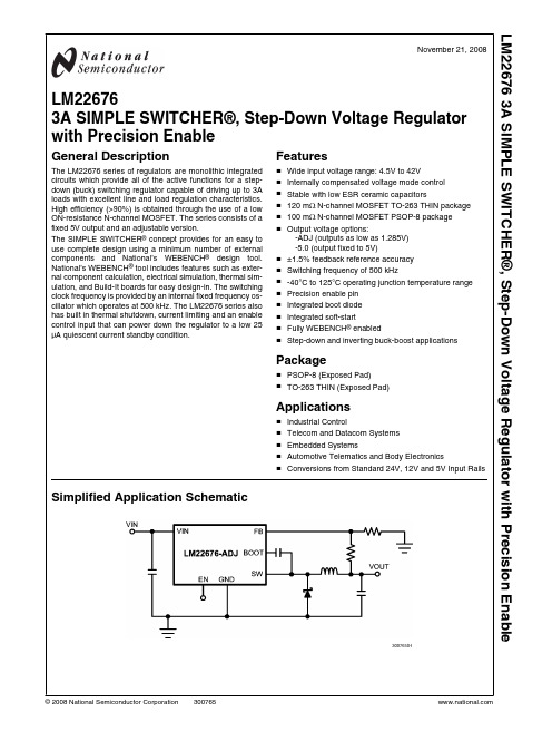
November 21, 2008 LM226763A SIMPLE SWITCHER®, Step-Down Voltage Regulator with Precision EnableGeneral DescriptionThe LM22676 series of regulators are monolithic integrated circuits which provide all of the active functions for a step-down (buck) switching regulator capable of driving up to 3A loads with excellent line and load regulation characteristics. High efficiency (>90%) is obtained through the use of a low ON-resistance N-channel MOSFET. The series consists of a fixed 5V output and an adjustable version.The SIMPLE SWITCHER® concept provides for an easy to use complete design using a minimum number of external components and National’s WEBENCH® design tool. National’s WEBENCH® tool includes features such as exter-nal component calculation, electrical simulation, thermal sim-ulation, and Build-It boards for easy design-in. The switching clock frequency is provided by an internal fixed frequency os-cillator which operates at 500 kHz. The LM22676 series also has built in thermal shutdown, current limiting and an enable control input that can power down the regulator to a low 25µA quiescent current standby condition.Features■Wide input voltage range: 4.5V to 42V■Internally compensated voltage mode control■Stable with low ESR ceramic capacitors■120 mΩ N-channel MOSFET TO-263 THIN package■100 mΩ N-channel MOSFET PSOP-8 package■Output voltage options:-ADJ (outputs as low as 1.285V)-5.0 (output fixed to 5V)■±1.5% feedback reference accuracy■Switching frequency of 500 kHz■-40°C to 125°C operating junction temperature range■Precision enable pin■Integrated boot diode■Integrated soft-start■Fully WEBENCH® enabled■Step-down and inverting buck-boost applications Package■PSOP-8 (Exposed Pad)■TO-263 THIN (Exposed Pad)Applications■Industrial Control■Telecom and Datacom Systems■Embedded Systems■Automotive Telematics and Body Electronics■Conversions from Standard 24V, 12V and 5V Input RailsSimplified Application Schematic30076501© 2008 National Semiconductor LM22676 3A SIMPLE SWITCHER®, Step-Down Voltage Regulator with Precision EnableConnection Diagrams300765408-Lead Plastic PSOP-8 Package NS Package Number MRA08B300765027-Lead Plastic TO-263 THIN PackageNS Package Number TJ7AOrdering InformationOutput VoltageOrder Number Package Type NSC Package DrawingSupplied As ADJ LM22676MR-ADJ PSOP-8 Exposed PadMRA08B95 Units in Rails ADJ LM22676MRE-ADJ 250 Units in Tape and Reel ADJ LM22676MRX-ADJ 2500 Units in Tape and Reel ADJ LM22676TJE-ADJ TO-263 THIN Exposed PadTJ7A250 Units in Tape and Reel ADJ LM22676TJ-ADJ 1000 Units in Tape and Reel5.0LM22676MR-5.0PSOP-8 Exposed PadMRA08B95 Units in Rails 5.0LM22676MRE-5.0250 Units in Tape and Reel 5.0LM22676MRX-5.02500 Units in Tape and Reel 5.0LM22676TJE-5.0TO-263 THIN Exposed PadTJ7A250 Units in Tape and Reel 5.0LM22676TJ-5.01000 Units in Tape and Reel 2L M 22676Pin DescriptionsPin Numbers PSOP-8Package Pin NumbersTO-263 THINPackageName Description Application Information13BOOT Bootstrap input Provides the gate voltage for the high side NFET.2, 35NC Not Connected Pins are not electrically connected inside the chip. Pins dofunction as thermal conductor.46FB Feedback pin Inverting input to the internal voltage error amplifier.57EN Precision enable pin When pulled low regulator turns off.64GND System ground Provide good capacitive decoupling between VIN and thispin72VIN Source input voltage Input to the regulator. Operates from 4.5V to 42V.81SW Switch pin Attaches to the switch nodeLM22676Absolute Maximum Ratings (Note 1)If Military/Aerospace specified devices are required,please contact the National Semiconductor Sales Office/Distributors for availability and specifications.VIN to GND 43VEN Pin Voltage-0.5V to 6V SW to GND (Note 2)-5V to V IN BOOT Pin Voltage V SW + 7V FB Pin Voltage -0.5V to 7V Power DissipationInternally LimitedJunction Temperature 150°CSoldering Information Infrared (5 sec.)260°CESD Rating (Note 3) Human Body Model±2 kVStorage Temperature Range -65°C to +150°COperating Ratings(Note 1)Supply Voltage (V IN )4.5V to 42V Junction Temperature Range-40°C to +125°CElectrical CharacteristicsLimits in standard type are for T J = 25°C only; limits in boldface type apply over thejunction temperature (T J ) range of -40°C to +125°C. Minimum and Maximum limits are guaranteed through test, design, or statistical correlation. Typical values represent the most likely parametric norm at T A = T J = 25°C, and are provided for reference purposes only. Unless otherwise specified: V IN = 12V.Symbol ParameterConditionsMin (Note 5)Typ (Note 4)Max (Note 5)UnitsLM22676-5.0V FBFeedback VoltageV IN = 8V to 42V4.925/4.95.05.075/5.1VLM22676-ADJV FB Feedback Voltage V IN = 4.7V to 42V 1.266/1.2591.285 1.304/1.311V All Output Voltage VersionsI Q Quiescent Current V FB = 5V 3.46mA I STDBY Standby Quiescent Current EN Pin = 0V 2540µA I CL Current Limit3.4/3.354.25.3/5.5A I L Output Leakage Current V IN = 42V, EN Pin = 0V, V SW = 0V 0.22µA V SW = -1V0.13µA R DS(ON)Switch On-Resistance TO-263 THIN Package 0.120.16/0.22ΩPSOP-8 Package 0.100.16/0.20f O Oscillator Frequency 400500600kHz T OFFMIN Minimum Off-time 300 ns T ONMIN Minimum On-time100 ns I BIAS Feedback Bias Current V FB = 1.3V (ADJ Version Only) 230 nA V EN Enable Threshold Voltage1.3 1.6 1.9V I EN Enable Input Current EN Input = 0V 6 µA T SD Thermal Shutdown Threshold150 °C θJA Thermal Resistance TJ Junction to ambient temperature resistance (Note 6)22 °C/W θJAThermal ResistanceMR Package, Junction to ambient temperature resistance (Note 7)60°C/W 4L M 22676Note 1:Absolute Maximum Ratings indicate limits beyond which damage to the device may occur, including inoperability and degradation of device reliability and/or performance. Functional operation of the device and/or non-degradation at the Absolute Maximum Ratings or other conditions beyond those indicated in the recommended Operating Ratings is not implied. The recommended Operating Ratings indicate conditions at which the device is functional and should not be operated beyond such conditions.Note 2:The absolute maximum specification of the ‘SW to GND’ applies to DC voltage. An extended negative voltage limit of -10V applies to a pulse of up to 50ns.Note 3:ESD was applied using the human body model, a 100 pF capacitor discharged through a 1.5 k Ω resistor into each pin.Note 4:Typical values represent most likely parametric norms at the conditions specified and are not guaranteed.Note 5:Min and Max limits are 100% production tested at 25°C. Limits over the operating temperature range are guaranteed through correlation using Statistical Quality Control (SQC) methods. Limits are used to calculate National’s Average Outgoing Quality Level (AOQL).Note 6:The value of θJA for the TO-263 THIN (TJ) package of 22°C/W is valid if package is mounted to 1 square inch of copper. The θJA value can range from 20 to 30°C/W depending on the amount of PCB copper dedicated to heat transfer. See application note AN-1797 for more information.Note 7:The value of θJA for the PSOP-8 exposed pad (MR) package of 60°C/W is valid if package is mounted to 1 square inch of copper. The θJA value can range from 42 to 115°C/W depending on the amount of PCB copper dedicated to heat transfer.Typical Performance CharacteristicsUnless otherwise specified the following conditions apply: Vin =12V, T J = 25°C.Efficiency vs I OUT and V INV OUT = 3.3V30076527Normalized Switching Frequency vs Temperature30076504Current Limit vs Temperature30076503Normalized R DS(ON) vs Temperature30076508LM22676Feedback Bias Current vs Temperature30076505Normalized Enable Threshold Voltage vs Temperature30076510Standby Quiescent Current vs Input Voltage 30076506Normalized Feedback Voltage vs Temperature30076507Normalized Feedback Voltage vs Input Voltage30076509 6L M 22676Typical Application Circuit and Block Diagram30076514FIGURE 1. 3.3V VOUT, 3A LM22676Detailed Operating DescriptionThe LM22676 switching regulator features all of the functions necessary to implement an efficient high voltage buck regu-lator using a minimum of external components. This easy to use regulator integrates a 42V N-Channel switch with an out-put current capability of 3A. The regulator control method is based on voltage mode control with input voltage feed for-ward. The loop compensation is integrated into the LM22676so that no external compensation components need to be se-lected or utilized. Voltage mode control offers short minimum on-times allowing short duty-cycles necessary in high input voltage applications. The operating frequency is fixed at 500kHz to allow for small external components while avoiding excessive switching losses. The output voltage can be set as low as 1.285V with the -ADJ device. Fault protection features include current limiting, thermal shutdown and remote shut-down capability. The device is available in the TO-263 THIN and PSOP-8 packages featuring an exposed pad to aid ther-mal dissipation.The functional block diagram with typical application of the LM22676 are shown in Figure 1.The internal compensation of the -ADJ option of the LM22676is optimized for output voltages up to 5V. If an output voltage of 5V or higher is needed, the -5.0 fixed output voltage option with an additional external resistive feedback voltage divider may also be used.Precision EnableThe precision enable pin (EN) can be used to shut down the power supply. Connecting this pin to ground or to a voltage less than typical 1.6V will completely turn off the regulator.The current drain from the input supply when off is typically 25 µA with 12V input voltage. The power consumed during this off state is mostly defined by an internal 2 M Ω resistor to VIN. The enable pin has an internal pull-up current source of approximately 6 µA. When driving the enable pin, the high voltage level for the on condition should not exceed the 6V absolute maximum limit. When enable control is not required,the EN pin should be left floating. The precision feature en-ables simple sequencing of multiple power supplies with a resistor divider from another power supply.Maximum Duty-Cycle / Dropout VoltageThe typical maximum duty-cycle is 85% at 500 kHz switching frequency. This corresponds to a typical minimum off-time of 300 ns. When operating at switching frequencies higher than 500 kHz, the 300 ns minimum off-time results in a lower max-imum duty-cycle limit than 85%. This forced off-time is impor-tant to provide enough time for the Cboot capacitor to charge during each cycle.The lowest input voltage required to maintain operation is:Where V D is the forward voltage drop across the re-circulating Schottky diode and V Q is the voltage drop across the internal power N-FET of the LM22676. The R DS(ON) of the FET is specified in the electrical characteristics section of this datasheet to calculate V Q according to the FET current. F is the switching frequency.Minimum Duty-CycleBesides a minimum off-time, there is also a minimum on-time which will take effect when the output voltage is adjusted very low and the input voltage is very high. Should the operation require a shorter minimum on-time than the typical 100 ns,individual switching pulses will be skipped.where D is the duty-cycle.Current LimitWhen the power switch turns on, the slight capacitance load-ing of the Schottky diode, D1, causes a leading-edge current spike with an extended ringing period. This spike can cause the current limit comparator to trip prematurely. A leading edge blanking time (T BLK ) of 110 ns (typical) is used to avoid sampling the spike.When the switch current reaches the current limit threshold,the switch is immediately turned off and the internal switching frequency is reduced. This extends the off time of the switch to prevent a steady state high current condition. As the switch current falls below the current limit threshold, the switch cur-rent will attempt to turn on. If a load fault continues, the switch will again exceed the threshold and turn off. This will result in a low duty-cycle pulsing of the power switch to minimize the overall fault condition power dissipation.The switching frequency will reduce (fold back) if the overload condition causes the output voltage to be 72.4% (typical) of the adjusted output voltage.The current limit will only protect the inductor from a runaway condition if the LM22676 is operating in its safe operating area. A runaway condition of the inductor is potentially catas-trophic to the application. For every design, the safe operating area needs to be calculated. Factors in determining the safe operating area are the switching frequency, input voltage,output voltage, minimum on-time and feedback voltage dur-ing an over current condition.As a first pass check, if the following equation holds true, a given design is considered in a safe operating area and the current limit will protect the circuit:V IN x T BLK x F < V OUT x 0.724If the equation above does not hold true, the following sec-ondary equation will need to hold true to be in safe operating area:If both equations do not hold true, a particular design will not have an effective current limit function which might damage the circuit during startup, over current conditions, or steady state over current and short circuit condition. Oftentimes a reduction of the maximum input voltage will bring a design into the safe operating area.Soft-StartThe soft-start feature allows the regulator to gradually reach the initial steady state operating point, thus reducing start-up stresses and surges. The soft-start is fixed to 500 µs (typical)start-up time and cannot be modified.8L M 22676Boot PinThe LM22676 integrates an N-Channel FET switch and as-sociated floating high voltage level shift / gate driver. This gate driver circuit works in conjunction with an internal diode and an external bootstrap capacitor. A 0.01 µF ceramic capacitor connected with short traces between the BOOT pin and the SW pin is recommended to effectively drive the internal FET switch. During the off-time of the switch, the SW voltage is approximately -0.5V and the external bootstrap capacitor is charged from the internal supply through the internal boot-strap diode. When operating with a high PWM duty-cycle, the buck switch will be forced off each cycle to ensure that the bootstrap capacitor is recharged. See the maximum duty-cy-cle section for more details.Thermal ProtectionInternal Thermal Shutdown circuitry protects the LM22676 in the event the maximum junction temperature is exceeded.When activated, typically at 150°C, the regulator is forced into a low power reset state. There is a typical hysteresis of 15degrees.Internal CompensationThe LM22676 has internal compensation designed for a sta-ble loop with a wide range of external power stage compo-nents.Insuring stability of a design with a specific power stage (in-ductor and output capacitor) can be tricky. The LM22676stability can be verified over varying loads and input and out-put voltages using WEBENCH® Designer online circuit sim-ulation tool at . A quick start spreadsheet can also be downloaded from the online product folder.The internal compensation of the -ADJ option of the LM22676is optimized for output voltages below 5V. If an output voltage of 5V or higher is needed, the -5.0 option with an additional external resistor divider may also be used.The typical location of the internal compensation poles and zeros as well as the DC gain is given in Table 1. The LM22676has internal type III compensation allowing for the use of most output capacitors including ceramics.This information can be used to calculate the transfer function from the FB pin to the internal compensation node (input to the PWM comparator in the block diagram).TABLE 1.Corners Frequency Pole 1150 kHz Pole 2250 kHz Pole 3100 Hz Zero 1 1.5 kHz Zero 215 kHz DC gain37.5 dBFor the power stage transfer function the standard voltage mode formulas for the double pole and the ESR zero apply:The peak ramp level of the oscillator signal feeding into the PWM comparator is V IN /10 which equals a gain of 20dB of this modulator stage of the IC. The -5.0 fixed output voltage option has twice the gain of the compensation transfer func-tion compared to the -ADJ option which is 43.5dB instead of 37.5dB.Generally, calculation as well as simulation can only aid in selecting good power stage components. A good design prac-tice is to test for stability with load transient tests or loop measurement tests. Application note AN-1889 shows how to easily perform a loop transfer function measurement with only an oscilloscope and a function generator.Application InformationEXTERNAL COMPONENTSThe following design procedures can be used to design a non-synchronous buck converter with the LM22676.InductorThe inductor value is determined based on the load current,ripple current, and the minimum and maximum input voltage.To keep the application in continuous current conduction mode (CCM), the maximum ripple current, I RIPPLE , should be less than twice the minimum load current.The general rule of keeping the inductor current peak-to-peak ripple around 30% of the nominal output current is a good compromise between excessive output voltage ripple and ex-cessive component size and cost. When selecting the induc-tor ripple current ensure that the peak current is below the minimum current limit as given in the Electrical Characteris-tics section. Using this value of ripple current, the value of inductor, L, is calculated using the following formula:where F is the switching frequency which is 500 kHz (typical).This procedure provides a guide to select the value of the inductor L. The nearest standard value will then be used in the circuit.Increasing the inductance will generally slow down the tran-sient response but reduce the output voltage ripple amplitude.Reducing the inductance will generally improve the transient response but increase the output voltage ripple.The inductor must be rated for the peak current, I PK+, to pre-vent saturation. During normal loading conditions, the peak current occurs at maximum load current plus maximum ripple.Under an overload condition as well as during load transients,the peak current is limited to 4.2A typical (5.5A maximum).This requires that the inductor be selected such that it can run at the maximum current limit and not only the steady state current.Depending on inductor manufacturer, the saturation rating is defined as the current necessary for the inductance to reduce by 30% at 20°C. In typical designs the inductor will run at higher temperatures. If the inductor is not rated for enough current, it might saturate and due to the propagation delay of the current limit circuitry, the power supply may get damaged.Input CapacitorGood quality input capacitors are necessary to limit the ripple voltage at the VIN pin while supplying most of the switch cur-rent during on-time. When the switch turns on, the current into the VIN pin steps to the peak value, then drops to zero at turn-9LM22676off. The average current into VIN during switch on-time is theload current. The input capacitance should be selected forRMS current, IRMS, and minimum ripple voltage. A good ap-proximation for the required ripple current rating necessary isIRMS> IOUT/ 2.Quality ceramic capacitors with a low ESR should be selectedfor the input filter. To allow for capacitor tolerances and volt-age effects, multiple capacitors may be used in parallel. If stepinput voltage transients are expected near the maximum rat-ing of the LM22676, a careful evaluation of ringing and pos-sible voltage spikes at the VIN pin should be completed. Anadditional damping network or input voltage clamp may berequired in these cases.Usually putting a higher ESR electrolytic input capacitor inparallel to the low ESR bypass capacitor will help to reduceexcessive voltages during a line transient and will also movethe resonance frequency of the input filter away from the reg-ulator bandwidth.Output CapacitorThe output capacitor can limit the output ripple voltage andprovide a source of charge for transient loading conditions.Multiple capacitors can be placed in parallel. Very low ESRcapacitors such as ceramic capacitors reduce the output rip-ple voltage and noise spikes, while larger higher ESR capac-itors in parallel provide large bulk capacitance for transientloading conditions. An approximation for the output voltageripple is:where ΔILis the inductor ripple current.Cboot CapacitorThe bootstrap capacitor between the BOOT pin and the SWpin supplies the gate current to turn on the N-channel MOS-FET. The recommended value of this capacitor is 10 nF andshould be a good quality, low ESR ceramic capacitor.It is possible to put a small resistor in series with the Cbootcapacitor to slow down the turn-on transition time of the in-ternal N-channel MOSFET. Resistors in the range of 10Ω to50Ω can slow down the transition time. This can reduce EMIof a switched mode power supply circuit. Using such a seriesresistor is not recommended for every design since it will in-crease the switching losses of the application and makesthermal considerations more challenging.Resistor DividerFor the -5.0 option no resistor divider is required for 5V outputvoltage. The output voltage should be directly connected tothe FB pin. Output voltages above 5V can use the -5.0 optionwith a resistor divider as an alternative to the -ADJ option.This may offer improved loop bandwidth in some applications.See the Internal Compensation section for more details.For the -ADJ option no resistor divider is required for 1.285Voutput voltage. The output voltage should be directly con-nected to the FB pin. Other output voltages can use the -ADJoption with a resistor divider.The resistor values can be determined by the following equa-tions:-ADJ option:-5.0 option:Where VFB= 1.285V typical for the -ADJ option and 5V for the-5.0 option30076523FIGURE 2. Resistive Feedback DividerA maximum value of 10 kΩ is recommended for the sum ofR1 and R2 to keep high output voltage accuracy for the –ADJoption. A maximum of 2 kΩ is recommended for the -5.0 out-put voltage option. For the 5V fixed output voltage option, thetotal internal divider resistance is typically 9.93 kΩ.At loads less than 5 mA, the boot capacitor will not holdenough charge to power the internal high side driver. Theoutput voltage may droop until the boot capacitor isrecharged. Selecting a total feedback resistance to be below3 kΩ will provide some minimal load and can keep the outputvoltage from collapsing in such low load conditions.Catch DiodeA Schottky type re-circulating diode is required for allLM22676 applications. Ultra-fast diodes which are not Schot-tky diodes are not recommended and may result in damageto the IC due to reverse recovery current transients. The nearideal reverse recovery characteristics and low forward volt-age drop of Schottky diodes are particularly important diodecharacteristics for high input voltage and low output voltageapplications common to the LM22676. The reverse recoverycharacteristic determines how long the current surge lastseach cycle when the N-channel MOSFET is turned on. Thereverse recovery characteristics of Schottky diodes mini-mizes the peak instantaneous power in the switch occurringduring turn-on for each cycle. The resulting switching lossesare significantly reduced when using a Schottky diode. Thereverse breakdown rating should be selected for the maxi-mum VIN, plus some safety margin. A rule of thumb is to selecta diode with the reverse voltage rating of 1.3 times the max-imum input voltage.The forward voltage drop has a significant impact on the con-version efficiency, especially for applications with a low outputvoltage. ‘Rated’ current for diodes varies widely from variousmanufacturers. The worst case is to assume a short circuitload condition. In this case the diode will carry the output cur-rent almost continuously. For the LM22676 this current canbe as high as 4.2A (typical). Assuming a worst case 1V drop 10LM22676across the diode, the maximum diode power dissipation can be as high as 4.2W.Circuit Board LayoutBoard layout is critical for switching power supplies. First, the ground plane area must be sufficient for thermal dissipation purposes. Second, appropriate guidelines must be followed to reduce the effects of switching noise. Switch mode con-verters are very fast switching devices. In such devices, the rapid increase of input current combined with the parasitic trace inductance generates unwanted L di/dt noise spikes. The magnitude of this noise tends to increase as the output current increases. This parasitic spike noise may turn into electromagnetic interference (EMI) and can also cause prob-lems in device performance. Therefore, care must be taken in layout to minimize the effect of this switching noise.The most important layout rule is to keep the AC current loops as small as possible. Figure 3 shows the current flow of a buck converter. The top schematic shows a dotted line which rep-resents the current flow during the FET switch on-state. The middle schematic shows the current flow during the FET switch off-state.The bottom schematic shows the currents referred to as AC currents. These AC currents are the most critical since current is changing in very short time periods. The dotted lines of the bottom schematic are the traces to keep as short as possible. This will also yield a small loop area reducing the loop induc-tance. To avoid functional problems due to layout, review the PCB layout example. Providing 3A of output current in a very low thermal resistance package such as the TO-263 THIN is challenging considering the trace inductances involved. Best results are achieved if the placement of the LM22676, the by-pass capacitor, the Schottky diode and the inductor are placed as shown in the example. It is also recommended to use 2oz copper boards or thicker to help thermal dissipation and to reduce the parasitic inductances of board traces.It is very important to ensure that the exposed DAP on the TO-263 THIN package is soldered to the ground area of the PCB to reduce the AC trace length between the bypass ca-pacitor ground and the ground connection to the LM22676. Not soldering the DAP to the board may result in erroneous operation due to excessive noise on the board.30076524FIGURE 3. Current Flow in a Buck ApplicationThermal ConsiderationsThe two highest power dissipating components are the re-circulating diode and the LM22676 regulator IC. The easiestmethod to determine the power dissipation within theLM22676 is to measure the total conversion losses (Pin –Pout) then subtract the power losses in the Schottky diodeand output inductor. An approximation for the Schottky diodeloss is:P = (1 - D) x IOUTx VDAn approximation for the output inductor power is:P = IOUT2 x R x 1.1,where R is the DC resistance of the inductor and the 1.1 factoris an approximation for the AC losses. The regulator has anexposed thermal pad to aid power dissipation. Adding severalvias under the device to the ground plane will greatly reducethe regulator junction temperature. Selecting a diode with anexposed pad will aid the power dissipation of the diode. Themost significant variables that affect the power dissipated bythe LM22676 are the output current, input voltage and oper-ating frequency. The power dissipated while operating nearthe maximum output current and maximum input voltage canbe appreciable. The junction-to-ambient thermal resistance ofthe LM22676 will vary with the application. The most signifi-cant variables are the area of copper in the PC board, thenumber of vias under the IC exposed pad and the amount offorced air cooling provided. The integrity of the solder con-nection from the IC exposed pad to the PC board is critical.Excessive voids will greatly diminish the thermal dissipationcapacity. The junction-to-ambient thermal resistance of theLM22676 TO-263 THIN and PSOP-8 packages are specifiedin the electrical characteristics table under the applicable con-ditions. For more information regarding the TO-263 THINpackage, refer to Application Note AN-1797 at.LM22676。
开关电源常用芯片

FSGM0765RWDTUFSL106HR 、FSL106MR 、FSL116LR 、开关电源常用芯片FSCQ1265RTYDTU 、 FSCQ1565RTYDTUFSDL321FSDH321 、FSDL0165RN 、FSDM0265RNB 、FSDH0265RN 、 FSDM0365RNB 、 FSDL0365RN 、 FSDM0465REWDTUFSDM0565REWDTU 、FSDM07652REWDTU FSDM311A 、FSEZ1016AMY 、 FSEZ1317NY 、Fairchild 仙童(飞兆)系列开关电源驱动芯片FAN100MY 、 FAN102MY 、FAN103MY 、 FAN6208 、 FAN6300AMY 、 FAN6754AMRMY 、FAN6862TY 、FAN6921MRMY 、FAN6961SZ 、FAN7346MX 、FAN7384MX 、 FAN7319MX 、FAN7527BMX 、FAN7527BN 、FAN7554N 、 FAN7554DFAN7621 、FAN7621SSJ 、FAN7621B 、FAN7631 、 FAN7930CMX ;FAN6204MYFL103 、FL6300A 即 FAN6300 、 FL6961 、FL7701 、FL7730 、FL7732 、FL7930B 、FLS0116 、FLS3217 、FLS3247 、FLS1600XS 、FLS1800XS 、 FLS2100XSFSFR1600 、 FSFR1600XSL 、 FSFR1700 、FSFR1700XS 、FSFR1700XSL 、FSFR1800 、 FSFR1800XS 、 FSFR1800XSL 、FSFR2100XSL 、FSFR2100FSCQ0565RTYDTU 、FSCQ0765RTYDTU、FSDM311 、FSEZ1317MYFSGM0465RWDTU 、FSGM0565RWDTUSD4569 )、ME8204 (兼容 SG6848 、OB2263 、OB2273 、 FSQ0565RSWDTUSG6105ADZ 、 SG6859ATZ 、SG5842KA5L0380RYDTU 、 KA5M0365RYDTUKA5M0365RTU 、KA5M0380RYDTU 、 KA3525A 、KA3842AC 、KA3842AE 、KA3842B 、KA3843B 、KA3844B 、 KA7500Con-bright 昂宝系列电源驱动芯片超低待机功耗产 品系列:OB5269、OB5269B 、OB2273、OB2273A 、OB2273B 、 OB2273F 、OB2273N 、OB2276 、OB2276A 原边控制系列产品: OB2520 、OB2520D 、OB2520M 、OB2532 、OB2531 ; OB2535/OB2535E 、OB2536/OB2536E 、OB2538/OB2538E OB2539 、OB2211 、OB2211H 、OB2212 、OB2216 准谐振 模式控制芯片系列: OB2201/T 、 OB2202 、 OB2203PWM 控制芯片系列产品: OB5269 、 OB5269B 、OB2273 、 OB2273A 、OB2273B 、OB2273F 、 OB2273N 、OB2361 、 OB2361P 、OB2262 、OB2263 、OB2268 、OB2269 、OB2279 、OB2287 、OB2288 、OB2298 、OB5222 、OB5225 、 OB2353/L 、OB2354/L 、OB2356/L 、OB2357/L 、OB2358/L 功率因子校正控制芯片: OB6573 、OB6572 、 OB6561P 、 OB6563 、OB6663LED 照明驱动系列: OB3330 、OB3340 、 OB3390/T 、 OB3391 、 OB3394 、OB3396 、OB3380 、 FSL206MRN 、FSL126MR 、FSL136MR 、FSQ100 、FSQ110 、 FSQ321 、FSQ510 、 FSQ0165RN 、 FSQ0170RNA 、 FSQ0265RN 、FSQ0270RNA 、FSQ0365RN 、FSQ0370RNA 、SN03ABCD 系列电源驱动芯片 PSR Controller :AP3703 、 AP3706 、AP3708N 、AP3760 、AP3765 、AP3766 、AP3768 、AP3769S 、AP3770 、AP3771 、AP3772Voltage Mode PWM Controller : AZ494A 、 AZ494C 、 AZ7500B 、 AZ7500C 、AZ7500E 、AZ7500FGreen Mode PWM Controller :AP3101 、AP3105/AP3105V/AP3105L/AP3105R AP3105/AP3105H ; AP3700 、 AP3700A 、AP3700E 、 AP3710Secondary Side Controller : AP4305 、 AP4306A 、AP4306B 、AP4313 、AP4310A 、 AP4340LED 照明 PFCME8101 (内置 13003 兼容THX203/RM6203/GW6203/CR6203 )、ME8105 (内置13003 兼容 THX203/RM6203/GW6203/CR6203机功能)、 ME8109A (内置 2N65 兼容 OB2358/AP8022 )、 ME8109B (内置 2N60 兼容 OB2358/AP8022 )、 ME8119 AP3102/AP3102V/AP3102L 、 AP3103 、、 AP3106 、 controller : AP1661/AP1661E AP1661A 、 AP1662 ; PSRcontroller : AP1681 (可调光)、 AP1682 、 AP1686microne 南京微盟系列开关电源驱动芯片 ME8100( 兼容 ATC30B ) 、,具有防炸(内置4N60 )、ME8110 (内置2N65 兼容OB2358 )、ME8200兼容SG6848 、OB2263 、LD7535 、GR8835 、SD456 )、ME8202 (兼容SG5841 、OB2269 、LD7552 、GR8841 、SD4569 )、ME8204 (兼容SG6848 、OB2263 、OB2273 、RM3261S 、 RM3261D 、RM3262D ; PFM 控制芯片系列: RM3252T 、 RM3260T 、RM3260DQR 控制芯片系列: RM6401S 、 RM6401D ;PFC+QR+PWM 控制芯片系列: RM6901S 、 RM6901Dchiplink-semi 南京芯联系列开关电源 驱动芯片 AC/DC PSR : CL1132 、CL1128 、 CL1101 、 LD7535 、 GR8835 、SD456 )、ME8300 (兼容 AP3708 )、 ME8302 (兼容 AP3768 )、ME8304 (兼容 AP3765 , AP3706 SOP8) )、ME8305 (内置 13003 兼容 AP3765 ,AP3706 SOP8) )、ME8315chiprail 成都启达系列开关电源驱动芯 片绿色节能 PWM/PFC 控制器: CR6848 、CR6850D 、 CR6853 、CR6842 、CR6845 、CR6855 、CR6232C 、CR6233 、CR5201 、CR6562 绿色节能 PWM 功率开关: CR5336 、CR5337 、CR5202 、CR5223 、CR5224 、CR5228 、 CR5229reactor-micro 陕西亚成微系列开关电源驱动芯片 RM3253S 、RM3253D 、RM3263S 、 RM3263D 、RM3261S 、RM3261D 、RM3262D 、RM3260T 、 RM3260D 、RM6203 、RM6204 、RM6221S 、 RM6221D 、 RM6222D 、RM6220T 、RM6401S 、RM6401S 、RM337X (1/2/3) 、RM3370T 、RM6901SPWM 功率开关芯片 RM6203D 、RM6204D 、RM6221S 、RM6221D 、 RM6222D ;PWM 控制芯片系列: RM6220TPFM 功率开关 RM3253S 、RM3253D 、RM3263S 、RM3263D 、 CR5335、 LED 照明驱动系列: 系列: 芯片系列:CL1100 ;PSR+MOS:CL1129 、CL1112 、CL1107 、CL1103PFC :CL6562 ;Flyback with MOSFET :CL1152 ;Flyback :CL1156 、CL1160 、CL1158Lighting LED Driver :CL0122 、CL0119A 、CL0118 、CL0116A 、CL0117 、CL6563A 、CL1158 、CL1112 、CL1129 、CL1128 、CL1101 、CL1100 、CL6809 、CL6808 、CL6807 、CL6804 ;Back Light Driver :CL6201sifirsttech 南海赛威系列开关电源驱动芯片AC/DC PWM Controller :SF1530 、SF1530U 、SF1531 、SF1531S 、SF1560 、SF1563 、SF1565 、SF1580 、SF1585 、SF1590 、SF1595 、SF5580 ;超低待机功耗AC/DC PWM 控制器IC :SF5533 、SF5534 、SF5545B 、SF5545 、SF5547AC/DC PWM Power Switch :SF1532 、SF1533 、SF1536 、SF1537 、SF1538 、SF1539 、SF1539HT 、SF1548 、SF1549 、SF5582H 、SF5582 、SF5590 ;原边反馈控制器/功率开关IC :SFL628 、SFL629 、SFL900 、SF5920S 、SF5920 、SF5922 、SF5922T 、西安民展微系列开关电源驱动芯片绿色节能PWM 功率转化、SF5922SV 、SF5926SV 、SF5926 、SF5928SV 、SF5922SSF5928S 、SF5928 、SF6010L 、SF6010F 、SF6018、SF6040 、SF6070 、SF6072 、SF6771 、SF6772 、SF6778 、SF6781 、SF6782 、SF6788 功率因子校正器IC :SFL320 、SF6562 、SFL500 、SF6563 、SF6566 ;LED 照明驱动IC :SFL330 、SFL520 、S FL668 、SFL669 、SFL678 、SF6010power-railSDC4569si-power 无锡硅动力系列开关电源驱动芯片SDC4569si-power 无锡硅动力系列开关电源驱动芯片PR6239 、CR6235S 、CR6236T 、 CR6238T 绿色节能 PWM 功率转化器系列 (PWM 控制芯片 + 600V MOSFET) 反激式 PR8224 、 PR8224H 、 CR6221T 、 CR6224S 、CR6224T 、CR6228T 、CR6229T 、 PR8612 绿 色节能 PWM 控制器系列 Primary Side Regulation 初级端 调节 PR6234 、CR6232PR6863 、PR9853 、 CR6850C 、 PR8278 、PR8278B 、PR8275 、PR6599 、PR6562 、CR6561 、CR6563 、PR8910 、PR3845Bbpsemi 上海晶丰明源系列开 关电源驱动芯片高功率因数高效率隔离恒流驱动芯片:BP2802 、 BP2808B 、BP2818 、 BP2812 、BP2822 高精度 BP3105 、BP3102 、 BP3122 、 BP3123 、BP3115 、BP3125 、 BP3108BP2309 、BP5118 、 BP1360 、BP1361 、BP1601maxictech 驱动芯片 MT7933 、MT7930 、MT7952 、MT7953 、MT7955 、 MT7950 、MT7801 、MT7838 、MT7200 、MT7201 、MT7261 、 MT7281 、MT7004Bsdc-semi 绍兴光大系列开关电源驱动芯 片 SDC602 、 SDC603 、SDC606 、SDC608 、SDC3842 、 SDC3843 、SDC3844 、SDC3845 、SDC4108 、SDC4108L 、 SDC4109 、 SDC4109L 、 SDC4563 、 SDC4565 、器系列 (PWM 控制芯片 + 600V MOSFET) 初级端调 节 :PR6237 、BP3309 、B P3308 高效率非隔离恒流驱动芯片: BP2808 、 高效率隔离恒流驱动芯片: 美芯晟系列开关电源SP5629P 、SP5619P 、SP5876P 、SP5876F 、SP5875P 、SP5875F 、SP5518F 、SP5808F 、5508F 、SP5506 、SP5505SP5615/6/8 可以代替OB2535/6/8 用于低功耗AC/DC 适配器的详细描述:SP5615 是一颗高精度离线式开关电源电路,应用于低功耗AC/DC 充电器与适配器。
欧泰顿摩勒尔系列NZM电气铝制电路保护器产品说明说明书

Eaton 265784Eaton Moeller series NZM - Molded Case Circuit Breaker. Circuit-breaker, 3p, 875A, N, 4Spécifications généralesEaton Moeller series NZM molded case circuit breaker electronic2657844015082657840401 mm 207 mm 210 mm 21 kg Eaton Selling Policy 25-000, one (1) year from the date of installation of theProduct or eighteen (18) months from thedate of shipment of the Product,whichever occurs first.RoHS conform IEC/EN 60947IECNZMN4-ME875Product NameCatalog NumberEANProduct Length/Depth Product Height Product Width Product Weight WarrantyCompliancesCertificationsModel Code875 AIs the panel builder's responsibility. The specifications for the switchgear must be observed.15 kA26 kAMeets the product standard's requirements.Is the panel builder's responsibility. The specifications for the switchgear must be observed.FixedBuilt-in device fixed built-in technique875 ADoes not apply, since the entire switchgear needs to be evaluated.10 segments of 80 mm x 1 mm (2x) at rear-side width extension Max. 10 segments of 32 mm x 1 mm (2x) at flat conductor terminal10 segments of 50 mm x 1 mm (2x) at 1-hole module plate Min. 5 segments of 25 mm x 1 mm at rear-side connection (punched)Max. 10 segments of 50 mm x 1 mm (2x) at rear-side connection (punched)Min. 6 segments of 16 mm x 0.8 mm at flat conductor terminal Rocker leverMeets the product standard's requirements.Product Data Sheet - NZMN4-ME875eaton-circuit-breaker-nzm-mccb-characteristic-curve-055.eps MN4-ME875IL01210010ZDA-CD-nzm4_3pDA-CS-nzm4_3pDA-DC-03_N4eaton-circuit-breaker-nzm-mccb-dimensions-022.epseaton-circuit-breaker-switch-nzm-mccb-3d-drawing-003.epseaton-manual-motor-starters-starter-msc-r-reversing-starter-wiring-diagram.epseaton-manual-motor-starters-starter-nzm-mccb-wiring-diagram.epsRated operational current for specified heat dissipation (In) 10.11 Short-circuit ratingRated short-circuit breaking capacity Ics (IEC/EN 60947) at 690 V, 50/60 HzRated short-circuit breaking capacity Icu (IEC/EN 60947) at 400/415 V, 50/60 Hz10.4 Clearances and creepage distances10.12 Electromagnetic compatibilityMounting MethodAmperage Rating10.2.5 LiftingTerminal capacity (copper strip)Handle type10.2.3.1 Verification of thermal stability of enclosures Caractéristiques Characteristic curve eCAD model Instructions d'installation mCAD modelRapports de certification SchémasSchémas électriques40 °CFitted with:Thermal protectionProtection against direct contactFinger and back-of-hand proof to VDE 0106 part 100Terminal capacity (copper busbar)Max. 80 mm x 10 mm (2x) at rear-side width extension50 mm x 10 mm (2x) at rear-side 2-hole module plateMin. 60 mm x 10 mm at rear-side width extensionM10 at rear-side screw connectionMin. 25 mm x 5 mm at rear-side 1-hole module plateMin. 25 mm x 5 mm direct at switch rear-side connection Max. 50 mm x 10 mm (2x) direct at switch rear-side connection Max. 50 mm x 10 mm (2x) at rear-side 1-hole module plate10.8 Connections for external conductorsIs the panel builder's responsibility.Special featuresIEC/EN 60947-4-1, IEC/EN60947-2The circuit-breaker fulfills allrequirements for AC-3switching category.R.m.s. value measurementand “thermal memory”Adjustable time delay settingto overcome current peaks trat 6 x Ir also infinity (withoutoverload releases)All AC-3 rating data appliesto direct switching by thecircuit-breaker under normaloperating conditions. If, forexample, a contactor takesover AC-3 switching undernormal operating conditions,the full rated uninterruptedcurrent applies to the circuit-breaker, In = Iu.Maximum back-up fuse, ifthe expected short-circuitcurrents at the installationlocation exceed theswitching capacity of thecircuit breaker (Rated short-Rated current = rateduninterrupted current: 875 AAmbient operating temperature - max70 °CClimatic proofingDamp heat, cyclic, to IEC 60068-2-30Damp heat, constant, to IEC 60068-2-78Terminal capacity (aluminum stranded conductor/cable)50 mm² - 240 mm² (4x) at 4-hole tunnel terminalTerminal capacity (copper stranded conductor/cable)120 mm² - 185 mm² (1x) direct at switch rear-side connection 50 mm² - 185 mm² (4x) direct at switch rear-side connectionLifespan, electrical3000 operations at 415 V AC-12000 operations at 400 V AC-32000 operations at 415 V AC-33000 operations at 400 V AC-11000 operations at 690 V AC-32000 operations at 690 V AC-1Electrical connection type of main circuitScrew connectionShort-circuit total breaktime< 25 ms ( 415 V); < 35 ms (> 415 V)Rated impulse withstand voltage (Uimp) at main contacts 8000 VRated short-circuit breaking capacity Ics (IEC/EN 60947) at 400/415 V, 50/60 Hz26 kA10.9.3 Impulse withstand voltageIs the panel builder's responsibility.Utilization categoryB (IEC/EN 60947-2)Number of polesThree-poleAmbient operating temperature - min-25 °C10.6 Incorporation of switching devices and components Does not apply, since the entire switchgear needs to be10.5 Protection against electric shockDoes not apply, since the entire switchgear needs to be evaluated.Terminal capacity (control cable)0.75 mm² - 1.5 mm² (2x)0.75 mm² - 2.5 mm² (1x)Equipment heat dissipation, current-dependent84.98 WClassMotor protectionInstantaneous current setting (Ii) - min875 A10.13 Mechanical functionThe device meets the requirements, provided the information in the instruction leaflet (IL) is observed.10.2.6 Mechanical impactDoes not apply, since the entire switchgear needs to be evaluated.10.9.4 Testing of enclosures made of insulating materialIs the panel builder's responsibility.Rated operational current588 A (690 V AC-3)820 A (400 V AC-3)Rated short-circuit breaking capacity Ics (IEC/EN 60947) at 230 V, 50/60 Hz37 kAApplicationUse in unearthed supply systems at 525 V10.3 Degree of protection of assembliesDoes not apply, since the entire switchgear needs to be evaluated.Interrupt rating50 kAIC at 400 VacRated short-circuit making capacity Icm at 240 V, 50/60 Hz105 kAFrameNZM4Rated short-circuit breaking capacity Ics (IEC/EN 60947) at 44026 kADegree of protection (IP), front sideIP66 (with door coupling rotary handle)IP40 (with insulating surround)Rated short-circuit making capacity Icm at 525 V, 50/60 Hz53 kARated short-circuit making capacity Icm at 690 V, 50/60 Hz40 kAInstantaneous current setting (Ii) - max12250 AOverload current setting (Ir) - min438 A10.2.3.2 Verification of resistance of insulating materials to normal heatMeets the product standard's requirements.10.2.3.3 Resist. of insul. mat. to abnormal heat/fire by internal elect. effectsMeets the product standard's requirements.Lifespan, mechanical10000 operationsOverload current setting (Ir) - max875 AVoltage rating690 V - 690 VTerminal capacity (copper solid conductor/cable)50 mm² - 240 mm² (4x) at 4-hole tunnel terminal95 mm² - 185 mm² (2x) at rear-side 2-hole module plate35 mm² - 185 mm² (4x) at rear-side 2-hole module plate300 mm² (4x) at rear-side width extension120 mm² - 300 mm² (1x) at rear-side 1-hole module plate95 mm² - 240 mm² (6x) at rear-side width extension95 mm² - 300 mm² (2x) at rear-side 1-hole module plateDegree of protection (terminations)IP00 (terminations, phase isolator and strip terminal)IP10 (tunnel terminal)10.9.2 Power-frequency electric strengthIs the panel builder's responsibility.Short-circuit release non-delayed setting - min1750 AIP20 (basic degree of protection, in the operating controls area) IP20Overvoltage categoryIIIRated short-time withstand current (t = 1 s)19.2 kARated impulse withstand voltage (Uimp) at auxiliary contacts 6000 VTerminal capacity (aluminum solid conductor/cable)240 mm² (2x) at rear-side width extension50 mm² (4x) at rear-side 2-hole module plate70 mm² - 185 mm² (2x) at rear-side 1-hole module plate70 mm² - 240 mm² (6x) at rear-side width extension185 mm² - 240 mm² (1x) at rear-side 1-hole module plateSwitch off techniqueElectronicRated short-time withstand current (t = 0.3 s)19.2 kAAmbient storage temperature - max70 °CRated short-circuit breaking capacity Ics (IEC/EN 60947) at 525 V, 50/60 Hz19 kAOptional terminalsConnection on rear. Strip terminal. Tunnel terminalRelease systemElectronic releasePollution degree310.7 Internal electrical circuits and connectionsIs the panel builder's responsibility.Rated operating power at AC-3, 230 V250 kWConnectionFront screw10.10 Temperature riseThe panel builder is responsible for the temperature rise calculation. Eaton will provide heat dissipation data for theFunctionsPhase failure sensitiveMotor protectionShort-circuit release non-delayed setting - max12250 AStandard terminalsScrew terminalRated short-circuit making capacity Icm at 400/415 V, 50/60 Hz 105 kARated operating power at AC-3, 400 V500 kWTypeCircuit breaker10.2.2 Corrosion resistanceMeets the product standard's requirements.10.2.4 Resistance to ultra-violet (UV) radiationMeets the product standard's requirements.10.2.7 InscriptionsMeets the product standard's requirements.Rated short-circuit making capacity Icm at 440 V, 50/60 Hz74 kAIsolation300 V AC (between the auxiliary contacts)500 V AC (between auxiliary contacts and main contacts)Number of operations per hour - max60Circuit breaker frame typeNZM4Direction of incoming supplyAs requiredShock resistance15 g (half-sinusoidal shock 11 ms)Rated insulation voltage (Ui)1000 VEaton Corporation plc Eaton House30 Pembroke Road Dublin 4, Ireland © 2023 Eaton. Tous droits réservés. Eaton is a registered trademark.All other trademarks areproperty of their respectiveowners./socialmedia。
贴片电阻标识代码表

Jumper ±1 ±2 ±5
<50mΩ .01Ω-10MegΩ .01Ω-10MegΩ .01Ω-10MegΩ
Jumper ±1 ±2 ±5
15V (DC or RMS)
Climatic category (IEC 60068)
55/125/56
Basic specification
IEC 601115-8
Description:
The resistors are constructed on a high grade ceramic body (aluminum oxide). Internal metal electrodes are added at each end and connected by a resistive paste which is applied to the top surface of the substrate. The composition of the paste is adjusted to give the approximate resistance required and the value is trimmed to within tolerance, by laser cutting of this resistive layer.
Features:
• Small size and light weight • Suitable for both flow and re-flow soldering • Reduction of assembly costs and matching with placement machines
Applications:
• Camcorders • Cellular • Hearing aids • Advanced pagers • Palmtop computers
敦泰触摸IC参数对照表
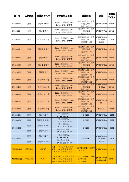
20*12
FT5402DQT
互容
推荐7-10.1寸
27*16
FT5206GE1
互容
推荐2.8-5寸
Sito:金属架桥,OGS Dito:G+G,G+F+F Sito:金属架桥,OGS Dito:G+G,G+F+F Sito:金属架桥,OGS Dito:G+G,G+F+F Sito:金属架桥,OGS Dito:G+G,G+F+F Sito:金属架桥,OGS Dito:G+G,G+F+F Sito:金属架桥,OGS Dito:G+G,G+F+F Sito:金属架桥,OGS Dito:G+G,G+F+F Sito:金属架桥,OGS Dito:G+G,G+F+F Sito:金属架桥,OGS Dito:G+G,G+F+F 横三角图案: GF,GG,OGS,GP,PF 横三角图案: GF,GG,OGS,GP,PF 横三角图案: GF,GG,OGS,GP,PF 竖三角2点图案: GF,GG,OGS,GP,PF 横三角图案: GF,GG,OGS,GP,PF 竖三角2点图案: GF,GG,OGS,GP,PF G1M – OGS结构单层互容 GFM – GF结构单层互容 GGM – GG结构单层互容 G1M – OGS 结构单层互容 GFM – GF结构单层互容 GGM – GG结构单层互容
工作电流:6mA 待机电流:4mA 睡眠电流:30uA
工作温度: -20~+85 储存温度: -55~+150 工作温度: -20~+85 储存温度: -55~+150
优恩半导体ESD静电保护器目录表

Part Number (Reference) ESD3.3V52D-A ESD05V52D-A ESD08V52D-A ESD12V52D-A ESD15V52D-A ESD24V52D-A ESD05V52D-C ESD12V52D-CInternal ConfigurationVrwm(V) 3.3 5 8 12 15 24 5 9Vbrmin(V)CJMAX 1MHz(pF) 200 110 70 60 50 25 10 5 450 200 30 100 75 50Peak Power Ir@Vrwm 8/20 µ s (µA) 120 120 120 120 120 120 100 100 320 320 100 320 320 320 200 5 5 5 5 5 1 1 40 10 1 1 1 1SOD-5234 6 8.5 13.3 16.6 26.7 6 10.2 4 6 6 13.3 16.7 26.7SOD-523 ESD03V32D-C ESD05V32D-C ESD0501V32D-C ESD12V32D-C ESD15V32D-C ESD24V32D-C 3 5 5 12 15 24SOD-323ESD3.3V32D-LA ESD05V32D-LA SOD-323 ESD03V32D-LC ESD05V32D-LC ESD08V32D-LC ESD12V32D-LC ESD15V32D-LC ESD24V32D-LC3.3 5.04 60.4 0.4350 35020 5SOD-3233.0 5.0 8.0 12.0 15.0 24.04.0 6.0 8.5 13.3 16.7 26.71.2 1.2 1.2 1.2 1.2 1.2350 350 350 350 350 35020 5 2 1 1 1ESD05V14TLC SOT-1435.06.01.23005Part Number (Reference) ESD03V23T-2A ESD05V23T-2A ESD05V23T-2AL ESD08V23T-2A ESD12V23T-2A ESD15V23T-2A ESD24V23T-2A ESD36V23T-2AInternal ConfigurationVrwm(V) 3.3 5.0 5.0 8.0 12.0 15.0 24.0 36.0Vbrmin(V)CJMAX 1MHz(pF) 400 300 30 250 150 100 88 60Peak Power Ir@Vrwm 8/20 µ s (µA) 300 300 100 300 300 300 300 300 100 10 0.1 1 1 1 1 1SOT-234.0 6.0 6.0 8.5 13.3 16.7 26.7 40.0ESD05V23T-2L SOT-23 Pin 3 to Pin1/Pin2 SM712 Pin 3 to Pin1/Pin2 ESD3.3V23T-1A ESD05V23T-1A ESD08V23T-1A ESD12V23T-1A ESD15V23T-1A ESD24V23T-1A ESD36V23T-1A SOT-235.06.01350177.555400107 3.3 5.0 8.0 12.0 15.0 24.0 36.013.3 4.0 6.0 8.5 13.3 16.7 24.0 40.055 5 5 5 5 5 5 5400 500 500 500 500 500 500 5001 40 5 5 1 1 1 1SOT-23SLVU2.8 SOT-232.83.034001ESD05V26T-4 SOT-265.06.01.23501Part Number (Reference) ESD05V26T-4L ESD12V26T-4L ESD15V26T-4L ESD24V26T-4LInternal ConfigurationVrwm(V)Vbrmin(V)CJMAX 1MHz(pF) 200 90 70 50Peak Power Ir@Vrwm 8/20 µ s (µA) 350 350 350 350 5 1 1 15.0 12.0 15.0 24.0 SOT-266.0 13.3 16.7 26.7ESD05V26T-5L ESD12V26T-5L ESD15V26T-5L ESD24V26T-5L SOT-265.0 12.0 15.0 24.06.0 13.3 16.7 26.7200 90 70 50350 350 350 3505 1 1 1ESD05V36T-4L SOT-3635.06.021501ESD05V36T-5L SOT-3635.06.0501001ESD05V56T-2L SOT-5635.06.00.9501ESD05V56T-4L SOT-5635.06.0301001ESD05V56T-5L SOT-5635.06.0301001Part Number (Reference)Internal ConfigurationVrwm(V)Vbrmin(V)CJMAX 1MHz(pF)Peak Power Ir@Vrwm 8/20 µ s (µA)ESD12V56T-2C SOT-5639.010.031001SLVU2.8-4 SO-082.83.024005SLVU2.8-8 SO-08 ESD06V08S-4L SO-082.83.0560056.06.825200020ESD05V08S-4L SO-08 LCDA05C-4 LCDA12C-4 LCDA15C-4 LCDA24C-45.06.0550010SO-085.0 12.0 15.0 24.06.0 13.3 16.7 26.75 5 5 5500 500 500 50020 1 1 1LCDA05C-8 LCDA12C-8 LCDA15C-8 LCDA24C-8 SO-165.0 12.0 15.0 24.06.0 13.3 16.7 26.75 5 5 5500 500 500 50020 1 1 1Part Number (Reference)Internal ConfigurationVrwm(V)Vbrmin(V)CJMAX 1MHz(pF)Peak Power Ir@Vrwm 8/20 µ s (µA)ESD05VDFN-C DFN10065.06.0101001ULC0524P DSON-105.06.00.81501ULC0528P5.06.50.52000.5MSOP-08ESD05V10S-4L MSOP-105.06.00.51251Cell Phone CCD Camera LinesEE0504K LWSON-085.06.020Color LCD Protection Clamshell Cell Phones0.5Cell Phone CCD Camera LinesESD0506K5.06.020Color LCD Protection Clamshell Cell Phones0.5LWSON-12Part Number (Reference)Internal ConfigurationVrwm(V)Vbrmin(V)CJMAX 1MHz(pF)Peak Power Ir@Vrwm 8/20 µ s (µA)Cell Phone CCD Camera LinesEE0508K5.06.020Color LCD Protection Clamshell Cell Phones0.5LWSON-16EE0508DFN5.06.0171DFN3014Differential Mode vs. Common Mode4345256162 of 211232011/3/31Curves of CharacterizationBAV99 vs TVS ARRAYS直接將突波導入到 Vcc -- 這種方式非 非 常不安全, 易導致 Vcc損害.直接將突波導入到 GND -- 這種方式非 非 常安全. 因為接地 區域有較大阻抗可 以分散突波.4 of 212011/3/31Parasitic InductanceESD ProtectorESD Protector不妥當的方式 : 無法將保護元件直接貼 在信號線上. 會產生寄 生電感. 造成保護能力 被寄生的電感減弱.安全的方式 : 將保護元件直接貼在信 號線上. 讓保護能力全 力發揮.Fine Layout vs Parasitic InductanceFine Layout -- Without Parasitic InductanceNOT recommation -- Parasitic Inductance7 of 212011/3/31Anti-Parasitic Inductance直接將保護ESD保護能力元件貼在信號線上--不會產生寄生電感問題.可以完全發揮8 of 212011/3/31Anti-Parasitic Inductance3-PIN產品的應用9 of 212011/3/31USB 3.0 Interface ProtectionMSOP-0810 of 212011/3/31HDMI Interface ProtectionSLP2510P8(2.5x1.0x0.5mm)11 of 212011/3/31USB 3.0 Interface Protection12 of 212011/3/31GR-1089 Lighting Protection for T-Carrier Interface13 of 212011/3/3110/1000 Gigabit Ethernet Protection14 of 212011/3/31。
- 1、下载文档前请自行甄别文档内容的完整性,平台不提供额外的编辑、内容补充、找答案等附加服务。
- 2、"仅部分预览"的文档,不可在线预览部分如存在完整性等问题,可反馈申请退款(可完整预览的文档不适用该条件!)。
- 3、如文档侵犯您的权益,请联系客服反馈,我们会尽快为您处理(人工客服工作时间:9:00-18:30)。
OB2536- MOJAY(茂捷)M5836替代书
OB2536可以被MOJAY(茂捷)M5836替代,
M5836具有电源软启动控制和多种带自动恢复的有效保护,它包含逐周期电流限制,VDD 过压保护,VDD箝位和欠压保护等。
另外,M5836还有优良的EMI性能和频率抖动控制特性,使用M5836可获得高精确的恒压恒流特性
极限参数
●全电压范围内,恒压调节精度误差<5%,恒流调节精度误差<5%
●原边采样和调节,无需光耦和TL431
●可编程CV和CC调节
●可设定恒流和输出功率
●内置原边反馈恒流控制
●内置自适应峰值电流调节
●内置原边变压器电感补偿
●可外部调整的输出线压降补偿
●开机软启动
●内置MOS开关管
●内置前沿消隐电路(LEB)
●可逐周期电流限制
●带有回差的欠压锁定(UVLO)
●VDD过压保护(OVP)
●VDD箝位功能
应用领域
适用于中小功率AC/DC离线式开关电源
●手机充电器
●数码相机充电器
●小功率适配器
●PC、TV等电器的辅助电源
●线性调节器/替代RCC变换器
●恒流LED照明
M583X是一颗高性价比开关电源芯片,用于低功耗离线式AC/DC电源适配器与电池充电器。
芯片通过原边取样来进行输出电压的调整,由此可以节省光耦与TL431。
M583X内置恒流/恒压控制电路,由此获得较高的恒流/恒压精度,可以满足绝大部分电源适配器与电池充电器的使用要求。
由于具有恒流特性,因此也可以应用于LED市场。
●启动电流和启动控制
M583X的启动电流非常低,所以VDD端电容电压可以很快充至开启电压。
启动电路中可以使用一个大阻值的电阻,在满足启动要求的同时,减小工作时的损耗。
●工作电流
M583X的工作电流低至2.5mA,所以VDD启动电容可以取更小值,同时借助于多工作模式的特点,可以提高整体效率。
●软启动
M583X内置有软启动功能,可以减少系统上电启动时各元器件的电压应力。
当VDD电压达到UVLO(OFF)时,芯片内部电路会将峰值电流阈值电压逐渐提升,具体来说是由接近于0V 提升至正常工作时的0.9V。
芯片的每一次重启都会伴随着这个软启动过程。
●恒流/恒压工作
M583X在充电器应用中,未充电的电池首先在恒流状态下进行充电,当电池将要充满时,充电阶段会转换为恒压模式。
在电源适配器的应用中,系统正常只工作于恒压状态。
在恒流模式下,系统限定了输出电流,并且不论输出电压如何下降,系统只确保输出电流恒定。
而在恒压模式下,系统通过原边取样来进行输出电压的调整。
●工作原理
为了确保实现M583X的恒流/恒压控制,反激电源系统需要设计工作于断续模式(DCM)下,具体可以参见前面的典型应用图1。
当反激系统工作于断续模式下,输出电压可以通过辅助线圈来取样。
在功率MOSFET导通阶段,负载由输出端电容Co来提供,此时原边电流上升。
当功率MOSFET关断时,原边电流按下述等式1.1
向副边传递:
Is=(Np/Ns)Ip (1)
辅助绕组电压如下式:
Vaux=(Naux/Ns)×(Vo+ΔV) (2)
通过在辅助线圈与INV(PIN 3)之间设置电阻分
压电路,辅助线圈的电压在每个消磁阶段将结束的时
候被采样,并且这个采样电压将会被保持直到下一个
采样周期。
采样电压与内部EA(误差放大器)的参考电压Vref(2.0V)进行比较,它们之间的误差将被放大。
EA的输出端COMP反映了负载情况,这个脚上的电压也决定了PWM的开关频率,通过这样一个闭环控制,M583X实现了对恒定输出电压的控制。
当取样电压低于Vref(2.0V),COMP脚电压达到最大值时,芯片进入恒流控制状态,开关频率直接由INV脚采样电压决定,实现了对恒定输出电流的控制。
●恒流和输出功率的调节
在M583X里,恒流点和最大输出功率可由CS端的采
样电阻RS来调节,见典型应用图,输出功率可以通过CC
点变化来调节,RS大,输出功率小,RS小,输出功率大,
说明见图3 。
●工作开关频率
M583X的开关频率是根据负载的条件和工作模式控制的,无需外部元件设定频率,最大输出功率时,开关频率为60KHz,在DCM方式反激工作情况下,最大输出功率可由下式给出: Po max=(1/2)LpFsw Lp²(3)
这里Lp为初级线圈电感,Ip为初级峰值电流,参考式(3),初级电感量的变化将导致最大输出功率的变化和恒流模式下输出电流的变化,为补偿初级电感偏差的变化,开关频率将有内部环路锁定,如下式:
Fsw=1/(2Tdemag) (4)
由于Tdemag和电感成反比,可使Ip和fsw乘积为恒定。
所以在恒流模式下,原边电感的变化不会影响最大输出功率和恒流输出,即可补偿初级电感偏差±10%以上。
● EMI频率抖动的改良
在M583X里,可以进行频率抖动控制(开关频率调制),从而分散噪声的频谱分布,分散的频谱将EMI减至最小,更容易设计系统。
●电流调节和输出波形毛刺处理
在M583X里,设置有逐周期电流限制电路,这个开关电流由CS脚上的采样电阻检测。
在功率MOS管打开初期,内部的前沿消隐电路可以消除采样信号中的电压尖峰,所以在CS 输入上不再需要外接RC滤波器,PWM占空周期由CS输入电压和EA输出电压决定。
●可设定的线压降补偿
在M583X内建了线压降补偿电路,以此取得更好的负载调整率。
内部的补偿电流流入外部电阻分压网络,由此在INV脚产生一个抵消电压。
补偿电流与COMP脚的电压成反比,也
就意味着与输出负载成反比,输出线压降补偿由此实现。
当输出由满载向空载变化时,INV 脚产生的补偿电压也会增大。
值得注意的是,通过改变INV脚分压网络中的电阻值,可以达到不同的补偿效果,获得所需的负载调整率。
图1中R5的推荐阻值范围为500Ω~4.7KΩ之间,R6根据式1.5计算:
……………………… 1.5
●保护控制
一个良好的电源系统,其可靠性好是必要的,即需要有一个完整的保护系统,主要包括逐周期电流限制(OCP),VDD箝位,电源软启动,欠电压锁定(UVLO)等。
VDD电压由辅助绕组产生,当VDD电压低于UVLO(ON)时M583X的输出就会关闭。
●。