AD9518-4ABCPZ-RL7;AD9518-4ABCPZ;AD9518-4APCBZ;中文规格书,Datasheet资料
ADI全部产品参考价格

本公司是专业化的电子元器件供应商,具有多年集成电路的销售经验,专业代理ADI公司全线产品,可广泛应用于通讯、汽车、家庭影院、投影电视、消费类音频、计算机和医疗等领域。
我公司所有产品均由美国原厂发货,稳定可靠、可代客订货,并提供免费样品和IC技术咨询服务。
我公司本着交货快捷,价格合理,诚实经营的理念,提供全面周到的配套服务,并在经营中不断完善自我,真诚欢迎新老客户及业界朋友前来咨询,并建立长期友好的合作关系。
如需了解更详细的价格,封装,最小起订量,库存数量,性能,技术参数,替代产品等信息,请访问我公司首页,使用站内搜索工具查询或联系我公司业务代表!公司主页:电话:0662-669217AD790AQ 59.28元/个AD790JN 31.90元/个AD790JNZ 28.94元/个AD790JR 31.90元/个AD790JR-REEL 31.90元/个AD790JR-REEL7 31.90元/个AD790JRZ 28.94元/个AD790JRZ-REEL 28.94元/个AD790JRZ-REEL 728.94元/个AD8561AN 15.05元/个AD8561ANZ 13.88元/个AD8561AR 15.05元/个AD8561AR-REEL 15.05元/个AD8561AR-REEL7 15.05元/个AD8561ARU-REEL 15.05元/个AD8561ARUZ 13.80元/个AD8561ARUZ-REEL 13.80元/个AD8561ARZ 13.80元/个AD8561ARZ-REEL 13.80元/个AD8561ARZ-REEL7 13.80元/个ADAU1513ACPZ 24.57元/个ADAU1513ACPZ-RL 24.57元/个ADAU1513ACPZ-RL7 24.57元/个EVAL-SSM2319Z 389.22元/个EVAL-SSM2335Z 393.90元/个SSM2335CBZ-REEL 4.91元/个SSM2335CBZ-REEL7 4.91元/个EVAL-SSM2335Z 393.90元/个SSM2335CBZ-REEL 4.91元/个SSM2335CBZ-REEL7 4.91元/个AD8564AN 32.06元/个AD8564ANZ 29.09元/个AD8564AR 32.06元/个AD8564AR-REEL 32.06元/个AD8564AR-REEL7 32.06 元/个AD8564ARU-REEL 32.06 元/个AD8564ARUZ-REEL 29.09元/个AD8564ARZ 29.09元/个AD8564ARZ-REEL 29.09 元/个AD8564ARZ-REEL7 元/个 AD8611AR 17.39元/个AD8611AR-REEL 17.39 元/个 AD8611AR-REEL7 17.39元/个 AD8611ARM-R2 17.39元/个AD8611ARM-REEL 17.39 元/个AD8611ARMZ-R2 15.76元/个 AD8611ARMZ-REEL 15.76元/个AD8611ARZ 15.76元/个AD8611ARZ-REEL 15.76元/个AD8611ARZ-REEL7 15.76元/个AD8612ARU 29.25元/个AD8612ARU-REEL 29.25 元/个AD8612ARUZ 26.60元/个AD8612ARUZ-REEL 26.60元/个8600804EA 8600804IA AD96685-REEL AD96685BH AD96685BP AD96685BP-REEL AD96685BQ AD96685BR 26.52元/个AD96685BR-REEL 26.52元/个AD96685BRZ 24.10 元/个AD96685BRZ-REEL 24.10元/个 AD96685TQ/883B 8293G160ARJZ-R2 9.20元/个AD8293G160ARJZ-R7 7.72元/个AD8293G160ARJZ-RL 元/个AD8293G160BRJZ-R2 12.87元/个AD8293G160BRJZ-R7 10.84元/个AD8293G160BRJZ-RL 元/个AD8295ACPZ-R 722.54元/个AD8295ACPZ-RL22.54元/个AD8295ACPZ-WP22.54元/个AD8295BCPZ-R7 33.85元/个AD8295BCPZ-RL 33.85元/个AD8295BCPZ-WP 33.85元/个AD8226ARMZ 元/个AD8226ARMZ-R7元/个AD8226ARMZ-RL 元/个AD8226ARZ元/个AD8226ARZ-R7元/个AD8226ARZ-RL 元/个AD8226BRMZ元/个AD8226BRMZ-R7元/个AD8226BRMZ-RL元/个AD8226BRZ元/个AD8226BRZ-R7元/个AD8226BRZ-RL元/个AD8293G80ARJZ-R2 9.20元/个AD8293G80ARJZ-R7 7.72元/个AD8293G80ARJZ-RL 元/个AD8293G80BRJZ-R2 12.87元/个AD8293G80BRJZ-R7 10.84元/个AD8293G80BRJZ-RL AD202JN 238.99元/个AD202JY 238.99元/个AD202KN 273.23元/个AD202KY 273.23元/个AD203SN 743.65元/个AD204JN 213.41元/个AD204JY213.41元/个AD204KN 247.57元/个AD208BY 585.16元/个AD208BY 666.35元/个AD210AN 418.31元/个AD210BN 503.72元/个AD210JN 375.65元/个AD215AY 384.15元/个AD215BY426.89元/个AD260AND-0 320.42元/个AD260AND-1 320.42元/个AD260AND-2 320.42元/个AD260AND-3 320.42元/个AD260AND-4 320.42元/个AD260AND-5 AD260BND-0 413.40元/个AD260BND-1 413.40元/个AD260BND-2 413.40元/个AD260BND-3 413.40元/个AD260BND-4 413.40元/个AD260BND-5 413.40元/个AD261AND-0 278.38元/个AD261AND-1 278.38元/个AD261AND-2 278.38元/个AD261AND-3 278.38元/个AD261AND-4 278.38元/个AD261AND-5 278.38元/个AD261BND-0 359.19元/个AD261BND-1 359.19元/个AD261BND-2 359.19元/个AD261BND-3 359.19元/个AD261BND-4 359.19元/个AD261BND-5 359.19元/个AD606JN 247.81元/个AD606JNZ 236.96元/个AD606JR 247.81元/个AD606JR-REEL7 247.81元/个AD606JRZ 236.96元/个AD606JRZ-REEL7 236.96元/个5962-9095501M2A8334AC114.35元/个AD8334ACPZ-REEL 114.35元/个AD8334ACPZ-REEL7 114.35元/个AD8335-EVALZ 2294.68元/个AD8335ACPZ 94.69元/个AD8335ACPZ-REEL 94.69元/个AD8335ACPZ-REEL7 94.69元/个AD8336-EVALZ 710.03元/个AD8336ACPZ-R7 36.27元/个AD8336ACPZ-RL35.80元/个AD8336ACPZ-WP 36.27元/个AD8337-EVALZ 642.56元/个AD8337-EVALZ-INV1055.57元/个AD8337-EVALZ-SS 1468.58元/个AD8337BCPZ-R2 19.66元/个AD8337BCPZ-REEL AD8337BCPZ-REEL7 19.66元/个AD8337BCPZ-WP 19.66元/个AD8350AR15 21.61元/个AD8350AR15-EVAL 781.48元/个AD8350AR15-REEL7 21.61元/个AD8350AR20 21.61元/个AD8350AR20-EVAL 781.48元/个AD8350AR20-REEL7 21.61元/个AD8350ARM15 21.61元/个AD8350ARM15-REEL7 21.61元/个AD8350ARM20 21.61元/个AD8350ARM20-REEL7 21.61元/个AD8350ARMZ15 19.66元/个AD8350ARMZ15-REEL7 19.66元/个AD8350ARMZ20 19.66元/个AD8350ARMZ20-REEL719.66元/个AD8350ARZ15-REEL7 19.66元/个AD8350ARZ20-REEL7 19.66元/个AD8351-EVALZ 781.48元/个AD8351ARM 23.09元/个AD8351ARM-REEL7 23.09元/个AD8351ARMZ 20.90元/个AD8351ARMZ-REEL7 20.90元/个AD8352-EVALZ 781.48元/个AD8352ACPZ-R2 AD8352ACPZ-R7 27.54 元/个AD8352ACPZ-WP 27.54元/个AD8366ACPZ-R7 AD8367-EVALZ AD8367ARU 39.55元/个AD8367ARU-REEL7 39.55元/个AD8367ARUZ 35.88元/个AD8367ARUZ-RL7 35.88元/个AD8368-EVALZ 781.48元/个AD8368ACPZ-REEL7 35.88元/个AD8368ACPZ-WP 35.88元/个AD8369-EVALZ 781.48元/个AD8369ARU 36.50元/个AD8369ARU-REEL7 36.50元/个AD8369ARUZ 33.15元/个AD8369ARUZ-REEL7 33.15元/个AD8370-EVALZ AD8370ARE 36.50元/个AD8370ARE-REEL7 36.50元/个AD8370AREZ 33.15元/个AD8370AREZ-RL7 33.15元/个AD8372-EVALZ AD8372ACPZ-R2 AD8372ACPZ-R7 51.32元/个AD8372ACPZ-WP 71.06元/个AD8375-EVALZ AD8375ACPZ-R7 35.41元/个AD8375ACPZ-WP 35.41元/个AD8376-EVALZ AD8376ACPZ-R7 51.25元/个AD8376ACPZ-WP 51.25元/个ADL5330-EVALZ 781.48元/个ADL5330ACPZ-R2 39.31元/个ADL5330ACPZ-REEL7 39.31元/个ADL5330ACPZ-WP 39.31元/个ADL5390-EVALZ 1560.00元/个ADL5390ACPZ-REEL7 59.20元/个ADL5390ACPZ-WP 59.20元/个ADL5391-EVALZ 1578.72元/个ADL5391ACPZ-R2 38.61元/个ADL5391ACPZ-R7 38.61元/个ADL5391ACPZ-WP 38.61元/个ADL5592-EVALZ ADL5592ACPZ-R7元/个ADA4859-3ACPZ-R2 15.52元/个ADA4859-3ACPZ-R7 15.52元/个ADA4859-3ACPZ-RL 15.52元/个ADA4856-3YCPZ-R2 12.79元/个ADA4856-3YCPZ-R7 10.84元/个ADA4856-3YCPZ-RL 10.84元/个ADA4420-6ARQZ 5.38元/个ADA4420-6ARQZ-R7 5.38元/个ADA4420-6ARQZ-RL 5.38元/个ADA4420-6ARUZ 元/个ADA4420-6ARUZ-R7元/个ADA4420-6ARUZ-R元/个AD800-52BR 184..16元/个AD800-52BRRL 元/个AD800-52BRZ 165.44元/个AD800-52BRZRL元/个AD60003RSZ24 AD60003RSZ24RL7元/个AD807A-155BR 108.89元/个AD807A-155BRRL 108.89元/个AD807A-155BRRL7 108.89元/个AD807A-155BRZ 98.98元/个AD807A-155BRZRL98.98元/个AD807A-155BRZRL7 98.98元/个AD60007 AD808-622BR 110.84元/个AD808-622BRRL AD808-622BRZ 100.70元/个AD808-622BRZRL7 ADN2804ACPZ 78.00元/个ADN2804ACPZ-500RL7 78.00元/个ADN2804ACPZ-RL7 78.00元/个EVAL-ADN2804EB 4538.82元/个ADN2805ACPZ 72.77元/个ADN2805ACPZ-500RL7 72.77元/个ADN2805ACPZ-RL7 72.77元/个EVAL-ADN2805EBZ 4538.82元/个ADN2806ACPZ 72.07元/个ADN2806ACPZ-500RL7 72.07元/个ADN2806ACPZ-RL7 72.07元/个EVAL-ADN2806EB 4538.82元/个ADN2807ACP 99.84元/个ADN2807ACPZ 90.79元/个ADN2807ACPZ-RL 90.79元/个EVAL-ADN2807-CML 4538.82元/个ADN2811ACP-CML292.03元/个ADN2811ACP-CML-RL292.03元/个ADN2811ACPZ-CML 292.03元/个EVAL-ADN2811-CML ADN2812ACP 468.86元/个ADN2812ACP-RL7 468.86元/个ADN2812ACPZ 426.27元/个ADN2812ACPZ-RL426.27元/个ADN2812ACPZ-RL7 426.27元/个EVAL-ADN2812-U2 EVAL-ADN2812EBZ 4538.92元/个ADN2813ACPZ 153.89元/个ADN2813ACPZ-500RL7 153.89元/个ADN2813ACPZ-RL7 153.89元/个EVAL-ADN2813EB 4538.82元/个ADN2814ACPZ 90.79元/个ADN2814ACPZ-500RL7 90.79元/个ADN2814ACPZ-RL7 90.79元/个EVAL-ADN2814EB 4538.82 元/个ADN2815ACPZ 138.53元/个ADN2815ACPZ-500RL7 138.53元/个ADN2815ACPZ-RL7 138.53元/个EVAL-ADN2815EB 4538.82元/个ADN2816ACPZ 83.15元/个ADN2816ACPZ-500RL7 93.91元/个ADN2816ACPZ-RL7 81.67元/个EVAL-ADN2816EB4538.82元/个ADN2817ACPZ 345.23元/个ADN2817ACPZ-RL ADN2817ACPZ-RL7 345.23元/个EVAL-ADN2817EB EVAL-ADN2817EBZ ADN2818ACPZ327.99元/个ADN2818ACPZ-RL ADN2818ACPZ-RL7 327.99元/个ADN2819ACP-CML390.70元/个ADN2819ACP-CML-RL 390.70元/个ADN2819ACPZ-CML355.21元/个ADN2819ACPZ-CML-RL 355.21元/个EVAL-ADN2819-CML AD9510-VCO/PCB AD9510-VCO/PCBZ 1184.04元/个AD9510/PCB AD9510/PCBZ 1184.04元/个AD9510BCPZ 94.30元/个AD9510BCPZ-REEL7 94.30元/个AD9511-VCO/PCB AD9511/PCB AD9511/PCBZ AD9511BCPZ 78.55元/个AD9511BCPZ-REEL7 78.55元/个AD9512/PCB 789.36元/个AD9512BCPZ 70.67元/个AD9512BCPZ-REEL7 70.67 元/个AD9513/PCB 786.70元/个AD9513/PCBZ 786.70元/个AD9513BCPZ 46.96元/个AD9513BCPZ-REEL7 46.96元/个AD9514/PCB 986.70元/个AD9514/PCBZ 986.70元/个AD9514BCPZ 46.96元/个AD9514BCPZ-REEL7 46.96元/个AD9515/PCB 986.70元/个AD9515/PCBZ 986.70元/个AD9515BCPZ 37.52元/个AD9515BCPZ-REEL7 37.52元/个AD9516-0/PCBZ 986.70元/个AD9516-0BCPZ 98.67元/个AD9516-0BCPZ-REEL7 98.67元/个AD9516-0/PCBZ 986.70元/个AD9516-0BCPZ 98.67 元/个AD9516-0BCPZ-REEL7 98.67元/个AD9516-1/PCBZ 986.70元/个AD9516-1BCPZ 98.67元/个AD9516-1BCPZ-REEL7 98.67元/个AD9516-2/PCBZ 986.70元/个AD9516-2BCPZ 98.67元/个AD9516-2BCPZ-REEL7 98.67元/个AD9516-3/PCBZ 986.70元/个AD9516-3BCPZ 98.67元/个AD9516-3BCPZ-REEL7 98.67元/个AD9516-4/PCBZ 986.70元/个AD9516-4BCPZ 98.67元/个AD9516-4BCPZ-REEL7 98.67元/个AD9517-0/PCBZ 986.70元/个AD9517-0BCPZ 90.01元/个AD9517-0BCPZ-REEL7 90.01元/个AD9517-1/PCBZ 986.70元/个AD9517-1BCPZ 90.01元/个AD9517-1BCPZ-REEL7 90.01元/个AD9517-2/PCBZ 986.70元/个AD9517-2BCPZ 90.01元/个AD9517-2BCPZ-REEL7 90.01元/个AD9517-3/PCBZ 986.70元/个AD9517-3BCPZ 90.01元/个AD9517-3BCPZ-REEL7 90.01元/个AD9517-4/PCBZ986.70元/个AD9517-4BCPZ 90.01元/个AD9517-4BCPZ-REEL7 90.01元/个AD9518-0/PCBZ 986.70元/个AD9518-0BCPZ 77.77元/个AD9518-0BCPZ-REEL7 77.77元/个AD9518-1/PCBZ 986.70元/个AD9518-1BCPZ 77.77元/个AD9518-1BCPZ-REEL7 77.77元/个AD9518-2/PCBZ 986.70元/个AD9518-2BCPZ 77.77元/个AD9518-2BCPZ-REEL7 77.77元/个AD9518-3/PCBZ 986.70元/个AD9518-3BCPZ 77.77元/个AD9518-3BCPZ-REEL7 77.77元/个AD9518-4/PCBZ 986.70元/个AD9518-4BCPZ 77.77元/个AD9518-4BCPZ-REEL7 77.77元/个AD9522-0/PCBZ元/个AD9522-0BCPZ 98.67元/个AD9522-0BCPZ-REEL7 98.67元/个AD9540-VCO/PCB 197.34元/个AD9540-VCO/PCBZ 197.34元/个AD9540/PCB 197.34元/个AD9540/PCBZ 197.34元/个AD9540BCPZ 78.55元/个AD9540BCPZ-REEL7 78.55元/个AD9549/PCBZ 986.70元/个AD9549BCPZ 97.97元/个AD9549BCPZ-REEL7 97.97元/个ADCLK905/PCBZ 986.70元/个ADCLK905BCPZ-R2 44.23元/个ADCLK905BCPZ-R7 44.23元/个ADCLK905BCPZ-WP 44.23元/个ADCLK907/PCBZ 986.70元/个ADCLK907BCPZ-R2 53.27元/个ADCLK907BCPZ-R7 53.27元/个ADCLK907BCPZ-WP 53.27元/个ADCLK925/PCBZ 986.70元/个ADCLK925BCPZ-R2 46.96元/个ADCLK925BCPZ-R7 46.96元/个ADCLK925BCPZ-WP 46.96元/个AD1955ARS 元/个AD1955ARSRL 元/个AD1955ARSZ 59.20元/个AD1955ARSZRL元/个EVAL-AD1955EBZ 3749.46元/个AD1853JRS元/个AD1853JRSRL元/个AD1853JRSZ 71.06元/个AD1853JRSZRL元/个AD1852JRSZ 63.18元/个AD1852JRSZRL AD1854JRS 52.10元/个AD1854JRSRL AD1854JRSZ 47.35元/个AD1854JRSZRL AD1854KRS 59.20元/个AD1854KRSRL元/个AD1933YSTZ 28.55元/个AD1933YSTZ-RL28.55元/个AD1833AASTZ 59.20元/个AD1833AASTZ-REEL元/个AD1833ACSTZ 34.32元/个AD1934YSTZ 24.57元/个AD1934YSTZ-RL 24.57元/个AD1851N AD1851N-J AD1851NZ AD1851NZ-J AD1851RAD1851R-J AD1851R-REEL7 AD1851RZ 55.07元/个AD1851RZ-J 59.20元/个AD1851RZ-REEL7 AD1859JR AD1859JR-REEL 56.16元/个AD1859JRS AD1859JRS-REEL56.16元/个AD1859JRZ AD1859JRZ-RL AD1866N AD1866NZ AD1866R AD1866R-REEL AD1866RZ 91.18元/个AD1866RZ-REEL AD5337ARM 9.59元/个AD5337ARM-REEL7 9.59元/个AD5337ARMZ 8.74元/个AD5337ARMZ-REEL7 8.74元/个AD5337BRM AD5337BRM-REEL 12.32元/个AD5337BRM-REEL7 12.32元/个AD5337BRMZ 12.32元/个AD5337BRMZ-REEL 12.32元/个AD5337BRMZ-REEL7 12.32元/个5962-9090801M2ADP2108ACPZ-2.3-R7 ADP2108ACPZ-2.5-R7 ADP2108ACPZ-3.0-R7 ADP2108ACPZ-3.3-R7 ADP2108AUJZ-1.0-R7 ADP2108AUJZ-1.1-R7 ADP2108AUJZ-1.2-R7 ADP2108AUJZ-1.3-R7 ADP2108AUJZ-1.5-R7 ADP2108AUJZ-1.8-R7 ADP2108AUJZ-1.82R7 ADP2108AUJZ-2.3-R7 ADP2108AUJZ-2.5-R7 ADP2108AUJZ-3.0-R7 ADP2108AUJZ-3.3-R7 ADP130-0.8-EVALZ 468.00元/个ADP1752-1.5-EVALZ 468.00元/个ADP1752ACPZ-0.75R7 7.02元/个ADP1752ACPZ-1.0-R7 7.02元/个ADP1752ACPZ-1.1-R7 7.02元/个ADP1752ACPZ-1.2-R7 7.02元/个ADP1752ACPZ-1.5-R7 7.02元/个ADP1752ACPZ-1.8-R7 7.02元/个ADP1752ACPZ-2.5-R7 7.02元/个ADP1753-EVALZ ADP1753ACPZ-R7 7.02元/个ADP1754-1.5-EVALZ 468.00元/个ADP1754ACPZ-0.75R7 7.41元/个ADP1754ACPZ-1.0-R7 7.41元/个ADP1754ACPZ-1.1-R7 7.41元/个ADP1754ACPZ-1.2-R7 7.41元/个ADP1754ACPZ-1.5-R7 7.41 元/个ADP1754ACPZ-1.8-R7 7.41元/个ADP1754ACPZ-2.5-R7 7.41元/个ADP1755-EVALZ ADP1755ACPZ ADP1755ACPZ-R7 7.41元/个ADP1740-1.5-EVALZ ADP1740-BL1-EVZADP1740 ACPZ-0.75R7 9.36元/个ADP1740ACPZ-1.0-R7 9.36元/个ADP1740ACPZ-1.1-R7 9.36元/个ADP1740ACPZ-1.2-R7 9.36元/个ADP1740ACPZ-1.5-R7 9.36元/个ADP1740ACPZ-1.8-R7 9.36元/个ADP1740ACPZ-2.5-R7 9.36元/个ADP1741-EVALZ ADP1741ACPZ ADP1741ACPZ-R7 ADP120-12-EVALZ 468.00元/个ADP120-15-EVALZ 468.00元/个ADP120-18-EVALZ 468.00元/个ADP120-33-EVALZ 468.00元/个ADP120-ACBZ12R7 2.26元/个ADP120-ACBZ155R7 ADP120-ACBZ15R7 2.26 元/个ADP120-ACBZ165R7 ADP120-ACBZ16R7 ADP120-ACBZ175R7 ADP120-ACBZ17R7 ADP120-ACBZ188R7 ADP120-ACBZ18R7 2.26元/个ADP120-ACBZ25R7 2.26元/个ADP120-ACBZ278R7 ADP120-ACBZ28R7元/个ADP120-ACBZ29R7 元/个ADP120-ACBZ33R7 ADP120-AUJZ12R7 2.03元/个元ADP120-AUJZ15R7 2.03/个ADP120-AUJZ18R7 2.03元/个ADP120-AUJZ33R7 2.03元/个ADP120-BL1-EVZ 78.00元/个ADP120CB-1.2-EVALZ ADP120CB-1.5-EVALZ ADP120CB-1.8-EVALZ ADP120CB-2.5-EVALZ ADP120CB-2.8-EVALZ ADP121-2.8-EVALZ ADP121-3.0-EVALZ 468.00元/个ADP121-3.3-EVALZ ADP121-ACBZ12R7ADP121-ACBZ155R7ADP121-ACBZ15R7ADP121-ACBZ165R7ADP121-AC BZ16R7 ADP121-ACBZ175R7 ADP121-ACBZ17R7 ADP121-ACBZ188R7 ADP121-ACBZ18R7 2.42元/个ADP121-ACBZ20R7 2.42元/个ADP121-ACBZ25R7 ADP121-ACBZ278R7 ADP121-ACBZ28R7 2.42元/个ADM1184ARMZ18.88元/个ADM1184ARMZ-REEL7 18.88元/个EVAL-ADM1184EBZ ADM1810-10AKS-RL7 3.98元/个ADM1810-10AKSZ-RL 3.59元/个ADM1810-10AKSZ-RL7 3.59元/个ADM1810-10ART-RL7 3.98元/个ADM1810-10ARTZ-RL 3.59元/个ADM1810-10ARTZ-RL7 3.59元/个ADM1810-5AKSZ-REEL 3.59元/个ADM1810-5AKSZ-RL7 3.59元/个ADM1810-5ART-REEL7 3.98 元/个ADM1810-5ARTZ-REEL 3.59元/个ADM1810-5ARTZ-RL7 ADM1811-10AKS-RL7 4.37元/个ADM1811-10AKSZ-RL ADM1811-10AKSZ-RL7 3.98元/个ADM1811-10ART-REEL 3.98元/个ADM1811-10ART-RL7 3.98元/个ADM1811-10ARTZ-RL 3.59元/个ADM1811-10ARTZ-RL7 3.59元/个ADM1811-5AKS-RL7 4.37元/个ADM1811-5AKSZ-REEL ADM1811-5AKSZ-RL7 3.98元/个ADM1811-5ART-REEL ADM1811-5ART-REEL7 3.98元/个ADM1811-5ARTZ-REEL ADM1811-5ARTZ-RL7 3.59元/个ADM1812-10AKS-RL7 4.37元/个ADM1812-10AKSZ-RL 3.98元/个ADM1812-10AKSZ-RL7 3.98元/个ADM1812-10ART-RL7 3.98元/个ADM1812-10ARTZ-RL 3.59元/个ADM1812-10ARTZ-RL7 3.59元/个ADM1812-5AKS-RL7 4.37元/个ADM1812-5AKSZ-REEL ADM1812-5AKSZ-RL7 3.98元/个ADM1812-5ART-REEL7 3.98元/个ADM1812-5ARTZ-REEL 3.59元/个ADM1812-5ARTZ-RL7 3.59元/个ADM1813-10AKS-REEL 3.43元/个ADM1813-10AKS-RL7 3..43元/个ADM1813-10AKSZ-RL 3.04元/个ADM1813-10AKSZ-RL7 3.04元/个ADM1813-10ART-REEL 3.43 元/个ADM1813-10ART-RL7 3.43元/个ADM1813-10ARTZ-RL 3.04元/个ADM1813-10ARTZ-RL7 3.04元/个ADM1813-5AKS-REEL 3.73元/个ADM1813-5AKS-RL7 3.73元/个ADM1813-5AKSZ-REEL 3.04元/个ADM1813-5AKSZ-RL7 3.04元/个ADM1813-5ART-RL7 3.43 元/个ADM1813-5ART-U1 ADM1813-5ARTZ-RL 3.04元/个ADM1813-5ARTZ-RL7 3.04元/个ADM1815-10AKS-RL7 ADM1815-10AKSZ-RL3.82元/个ADM1815-10AKSZ-RL7 3.51元/个ADM1815-10ART-REEL 3.51元/个ADM1815-10ART-RL7 ADM1815-10ARTZ-RL 3.43元/个ADM1815-10ARTZ-RL7 ADM1815-20AKSZ-RL3.51元/个ADM1815-20AKSZ-RL7 3.51元/个ADM1815-20ART-RL7 ADM1815-20ARTZ-RL7 ADM1815-5AKS-RL7 3.51元/个ADM1815-5AKSZ-REEL 3.51 元/个ADM1815-5AKSZ-RL7 ADM1815-5ART-REEL7 3.43元/个ADM1815-5ARTZ-REEL 3.04元/个ADM1815-R22AKSZ-R7 3.82元/个ADM1815-R22AKSZ-RL 3.51 元/个ADM1815-R22ART-RL7 3.43元/个ADM1815-R22ARTZ-R7 3.04元/个ADM1815-R22ARTZ-RL 3.04元/个ADM1815-R23AKSZ-R7 3.82元/个ADM1816-10AKSZ-RL3.98元/个ADM1816-10AKSZ-RL7 3.98 元/个ADM1816-10ART-REEL 3.98元/个ADM1816-10ART-RL7 3.98元/个ADM1816-10ARTZ-RL 3.59元/个ADM1816-10ARTZ-RL7 3.59元/个ADM1816-20AKS-RL7 3.98元/个ADM1816-20AKSZ-RL 3.59元/个ADM1816-20AKSZ-RL7 3.98元/个ADM1816-20ART-RL7 3.98元/个ADM1816-20ARTZ-RL 3.59元/个ADM1816-20ARTZ-RL7 3.59元/个ADM1816-5AKS-REEL7 3.98元/个ADM1816-5AKSZ-REEL 3.90 元/个ADM1816-5AKSZ-RL7 3.90元/个ADM1816-5ART-REEL7 3.59 元/个ADM1816-5ARTZ-REEL 3.59 元/个ADM1816-5ARTZ-RL7 3.59元/个ADM1816-R22AKS-RL7 4.37元/个ADM1816-R22AKSZ-R7 3.98 元/个ADM1816-R22AKSZ-RL3.98元/个ADM1816-R22ART-RL7 3.98元/个ADM1816-R22ARTZ-R7 3.59元/个ADM1816-R22ARTZ-RL 3.59元/个ADM1816-R23AKSZ-R7 ADM1816-R23AKSZ-RL3.98元/个ADM1816-R23ART-RL7 3.98元/个ADM1816-R23ARTZ-R7 3.59元/个ADM1816-R23ARTZ-RL 3.59 元/个ADM1817-10AKS-RL7 4.37元/个ADM1817-10AKSZ-RL 3.98 元/个ADM1817-10AKSZ-RL7 3.98元/个ADM1817-10ART-REEL 3.98元/个ADM1817-10ART-RL7 3.98元/个ADM1817-10ARTZ-RL3.59元/个ADM1817-10ARTZ-RL7 3.59元/个ADM1817-20AKS-RL7 ADM1817-20AKSZ-RL3.98元/个ADM1817-20AKSZ-RL7 3.98元/个ADM1817-20ART-RL7 ADM1817-20ARTZ-RL3.59元/个ADM1817-20ARTZ-RL7 3.59元/个ADM1817-5AKSZ-REEL 3.90元/个ADM1817-5AKSZ-RL7 3.90元/个ADM1817-5ART-REEL7 3.59元/个ADM1817-5ARTZ-REEL 3.59元/个ADM1817-5ARTZ-RL7 3.59元/个ADM1817-R22AKS-RL ADM1817-R22AKSZ-R7 3.90元/个ADM1817-R22AKSZ-RL 3.90元/个ADM1817-R22ART-RL7 3.59元/个ADM1817-R22ARTZ-R7 3.59元/个ADM1817-R22ARTZ-RL 3.59元/个ADM1817-R23AKS-RL ADM1817-R23AKSZ-R7 3.98元/个ADM1817-R23AKSZ-RL 3.98元/个ADM1817-R23ART-RL7 3.98元/个ADM1817-R23ARTZ-R7 3.59元/个ADM1817-R23ARTZ-RL 3.59元/个ADM1818-10AKS-RL7 ADM1818-10AKSZ-RL 3.59 元/个ADM1818-10AKSZ-RL7 3.59元/个ADM1818-10ARTZ-RL7 3.51元/个ADM1818-20AKSZ-RL ADM1818-20AKSZ-RL7 ADM1818-20ART-REEL 3.98元/个ADM1818-20ART-RL7 3.98元/个ADM1818-20ARTZ-RL7 3.98元/个ADM1085AKS-REEL7 2.89元/个ADM1085AKSZ-REEL7 3.65元/个ADM1086AKS-REEL7 2.89元/个ADM1086AKS-U1 ADM1086AKSZ-REEL7 2.65元/个ADM1087AKS-REEL7 2.89元/个ADM1087AKSZ-REEL7 2.65元/个EVAL-ADM1087EBZ 1184.04 元/个ADM1088AKSZ-REEL7 ADM1184ARMZ 18.88元/个ADM1184ARMZ-REEL7 18.88元/个EVAL-ADM1184EBZ ADM1185ARMZ-1 9.44元/个ADM1185ARMZ-1REEL7 9.44元/个EVAL-ADM1185EBZ 1184.04元/个ADM1186-1ARQZ 30.03元/个ADM1186-1ARQZ-REEL 30.03元/个ADM1186-2ARQZ 23.56元/个ADM1186-2ARQZ-REEL23.56元/个EVAL-ADM1186-1EBZ 1262.98元/个EVAL-ADM1186-1MBZ 236.81元/个EVAL-ADM1186-2EBZ 1262.98元/个EVAL-ADM1186-2MBZ 236.81元/个ADM6819ARJZ-REEL7 9.44元/个ADM6820ARJZ-REEL7 9.44元/个ADM1060ARU 56.47 元/个ADM1060ARU-REEL 56.47元/个ADM1060ARU-REEL7 56.47元/个ADM1060ARUZ 51.32元/个ADM1060ARUZ-REEL751.32元/个EVAL-ADM1060EBZ 1973.40元/个ADM1062ACP 65.13元/个ADM1062ACPZ 71.06元/个ADM1062ACPZ-REEL7 71.06元/个ADM1062ASU 65.13元/个ADM1062ASUZ 59.20元/个ADM1062ASUZ-REEL7 59.20元/个EVAL-ADM1062LFEBZ 2368.08元/个EVAL-ADM1062TQEBZ 2368.08元/个ADM1063ACP 71.68 元/个ADM1063ACPZ 65.13元/个ADM1063ACPZ-REEL7 65.13元/个ADM1063ASU 71.68元/个ADM1063ASUZ 65.13元/个ADM1063ASUZ-REEL7 65.13元/个EVAL-ADM1063LFEBZ 2368.08元/个EVAL-ADM1063TQEBZ 2368.08元/个ADM1064ACP 67.31元/个ADM1064ACP-REEL 67.31元/个ADM1064ACP-REEL7 67.31元/个ADM1064ACPZ 61.07元/个ADM1064ASU 67.31元/个ADM1064ASU-REEL 67.31元/个ADM1064ASU-REEL7 67.31元/个ADM1064ASUZ 61.15元/个EVAL-ADM1064LFEBZ 2604.89元/个EVAL-ADM1064TQEBZ 2368.08元/个ADM1065ACP49.50元/个ADM1065ACP-REEL7 49.50元/个ADM1065ACPZ 45.40元/个ADM1065ASU49.50元/个ADM1065ASU-REEL7 49.50元/个ADM1065ASUZ 45.40元/个EVAL-ADM1065LFEBZ 2368.08元/个EVAL-ADM1065TQEBZ 2368.08元/个ADM1066ACP 73.79元/个ADM1066ACP-REEL 73.79元/个ADM1066ACP-REEL7 73.79元/个ADM1066ACPZ 67.08元/个ADM1085AKS-REEL7 2.89元/个ADM1085AKSZ-REEL7 2.65元/个ADM1086AKS-REEL7 2.89元/个ADM1086AKS-U1 ADM1086AKSZ-REEL7 2.65元/个ADM1087AKS-REEL7 2.89 元/个ADM1087AKSZ-REEL7 2.65元/个EVAL-ADM1087EBZ 1184.04元/个ADM1184ARMZ 18.88元/个ADM1184ARMZ-REEL7 18.88元/个EVAL-ADM1184EBZ ADM1185ARMZ-1 9.44元/个ADM1185ARMZ-1REEL7 9.44元/个EVAL-ADM1185EBZ 1184.04元/个ADM1186-1ARQZ 30.03元/个ADM1186-1ARQZ-REEL 30.03元/个ADM1186-2ARQZ 23.57元/个ADM1186-2ARQZ-REEL 23.57元/个EVAL-ADM1186-1EBZ 1262.98元/个EVAL-ADM1186-1MBZ 236.81元/个EVAL-ADM1186-2EBZ 1262.98元/个EVAL-ADM1186-2MBZ 236.81元/个ADM1185ARMZ-1 9.44元/个ADM1185ARMZ-1REEL7 9.44元/个EVAL-ADM1185EBZ 1184.04元/个ADM1186-1ARQZ 30.03元/个ADM1186-1ARQZ-REEL 30.03元/个ADM1186-2ARQZ ADM802LARN 20.83元/个ADM802LARNZ 18.95元/个ADM802LARNZ-REEL ADM802MAN ADM802MANZ 18.95 元/个ADM802MARN 20.83元/个ADM802MARNZ18.95元/个ADM805LAN20.83元/个ADM805LANZ 18.95元/个ADM805LARN20.83元/个ADM805LARNZ 18.95 元/个ADM805LARNZ-REEL ADM805MARN ADM690AN 24.41元/个ADM690ANZ 22.15元/个ADM690AAN 18.10元/个ADM690AANZ 16.38 元/个ADM690AARM16.22元/个ADM690AARMZ 14.74 元/个ADM690AARMZ-REELADM690AARN 18.10元/个ADM690AARN-REEL ADM690AARNZ16.38元/个ADM690AARNZ-REEL ADM691AN 27.07 元/个ADM691ANZ 24.65元/个ADM691AQ47.81元/个ADM691AR 28.86 元/个ADM691AR-REEL ADM691AR-REEL7 ADM691ARZ 26.29元/个ADM691ARZ-REEL ADM691ARZ-REEL7 ADM691SQ 54.99元/个ADM694AN 25.27元/个ADM694ANZ 22.93元/个ADM695AN 27.07元/个ADM695ANZ 24.65元/个ADM695AQ 47.81元/个ADM695AR 30.26元/个ADM695AR-REELADM695ARZ 27.46元/个ADM695ARZ-REEL ADM8690AN 23.95元/个ADM8690ANZ 21.68元/个ADM8690ARN 23.95元/个ADM8690ARN-REEL ADM8690ARNZ 21.68元/个ADM8691AN 28.63元/个ADM8691ANZ 26.05元/个ADM8691ARN 28.63元/个ADM8691ARN-REEL ADM8691ARNZ 26.05元/个ADM8691ARU 28.63元/个ADM8691ARU-REEL ADM8691ARUZ 26.05元/个ADM8691ARW 28.63元/个ADM8691ARWZ 26.05 元/个ADM8695ARW-REEL ADM8695ARWZ 21.29元/个ADM660AN 16.54元/个ADM660ANZ 14.98元/个ADM660AR 16.54 元/个ADM660AR-REEL ADM660ARU 16.54元/个ADM660ARU-REEL ADM660ARU-REEL7 ADM660ARUZ 14.98元/个ADM660ARUZ-REEL ADM660ARUZ-REEL7 ADM660ARZ 14.98元/个ADM660ARZ-REEL ADM8660AN 17.39元/个ADM8660ANZ 15.76元/个ADM8660AR 17.39元/个ADM8660ARZ 15.76元/个ADM8828ART-REEL 6.55元/个ADM8828ART-REEL7 6.55元/个ADM8828ARTZ-REEL 5.93元/个ADM8828ARTZ-REEL7 5.93 元/个ADM8829ARTZ-REEL 5.93元/个ADM8829ARTZ-REEL7 5.93元/个ADM8832-EVALZ ADM8832ACP 17.39元/个ADM8832ACP-REEL 17.39元/个ADM8832ACP-REEL7 17.39元/个ADM8832ACPZ 15.76元/个ADM8832ACPZ-REEL 15.76 元/个ADM8832ACPZ-REEL7 15.76元/个ADM8832EB-EVALZ 1184.04元/个ADM8839-EVALZ 473.62 元/个ADM8839ACP 16.64元/个ADM8839ACP-REEL ADM8839ACP-REEL7 16.64元/个ADM8839ACPZ 14.98元/个ADM8839ACPZ-REEL 14.98元/个ADM8839ACPZ-REEL7 14.98 元/个ADP3605AR 11.70元/个ADP3605AR-3 11.70元/个ADP3605AR-3-REEL 11.70元/个ADP3605AR-REEL 11.70 元/个ADP3605ARU-3-REEL 12.25元/个ADP3605ARU-3-REEL7 12.25元/个ADP3605ARU-REEL ADP3605ARU-REEL7 ADP3605ARUZ-3-REEL 12.25元/个ADP3605ARZ 11.70元/个ADP3605ARZ-3 ADP3605ARZ-3-REEL ADP1621-EVALZ 473.62元/个ADP1621ARMZ-R7 10.30 元/个ADP1821-EVAL 473.62元/个ADP1821-EVALZ 473.62 元/个ADP1821ARQZ-R7 10.69 元/个ADP1822-EVAL 473.62元/个ADP1822ARQZ-R7 11.08元/个ADP1823-EVAL 473.62元/个ADP1823ACPZ-R7 16.61元/个ADP1828HC-EVALZ 631.49元/个ADP1828LC-EVALZ 631.49元/个ADP1828YRQZ-R7 11.86元/个ADP1829-EVALZ 473.62 元/个ADP1829ACPZ-R7 16.61元/个ADP1864-BL-EVALZ 117.00元/个ADP1864-EVAL 473.62元/个ADP1864-EVALZ 473.62 元/个ADP1864AUJZ-R7 8.29元/个ADP1111AN 18.80元/个ADP1111AN-12 18.80元/个ADP1111AN-3.3 18.80元/个ADP1111AN-5 18.80元/个ADP1111ANZ 17.08元/个ADP1111ANZ-12 17.08元/个ADP1111ANZ-3.3 17.08 元/个ADP1111ANZ-5 17.08元/个ADP1111AR 17.94元/个ADP1111AR-12 17.94元/个ADP1111AR-12-REEL 17.94元/个ADP1111AR-3.3 17.94 元/个ADP1111AR-3.3-REEL 17.94元/个ADP1111AR-5 17.94元/个ADP1111AR-5-REEL 17.94元/个ADP1111AR-REEL 17.94 元/个ADP1111ARZ 15.99元/个ADP1111ARZ-12 15.99元/个ADP1111ARZ-12-REEL 15.99元/个ADP1111ARZ-3.3 15.99元/个ADP1111ARZ-5 15.99 元/个ADP1111ARZ-5-REEL 15.99元/个ADP1111ARZ-REEL ADP2108-1.0-EVALZ ADP2108-1.1-EVALZ 468.00 元/个ADP2108-1.2-EVALZ 468.00 元/个ADP2108-1.3-EVALZ 468.00元/个ADP2108-1.5-EVALZ 468.00 元/个ADP2108-1.8-EVALZ 468.00元/个ADP2108-1.82-EVALZ 468.00元/个AD1974YSTZ 31.28元/个AD1974YSTZ-RL 31.28 元/个EVAL-AD1974EBZ 1315.63元/个AD1871YRS AD1871YRS-REEL AD1871YRSZ 44.46元/个AD1871YRSZ-REEL EVAL-ADAU1871EBZ AD1877JR AD1877JRZ 66.30元/个AD1870AR AD1870AR-REEL AD1870ARZ AD1870ARZ-REEL AD7151BRMZ10.69元/个AD7151BRMZ-REEL 10.69元/个AD7156BCPZ-REEL 9.75元/个AD7156BCPZ-REEL7 9.75元/个EVAL-AD7156EBZ 548.57元/个AD7150BRMZ 10.69元/个AD7150BRMZ-REEL 10.69 元/个EVAL-AD7150EBZ 548.57元/个AD7148ACPZ-1500RL7 9.44 元/个AD7148ACPZ-1REEL 9.44元/个AD7143ACPZ-1500RL7 9.75元/个AD7143ACPZ-1REEL 9.75元/个AD7147ACPZ-1500RL7 10.30元/个AD7147ACPZ-1REEL 10.30元/个AD7147ACPZ-500RL7 10.30元/个AD7147ACPZ-REEL 10.30元/个AD7147PACPZ-1500R7 10.30元/个EVAL-AD7147-1EBZ 1381.38元/个EVAL-AD7147EBZ 1381.38元/个AD7142ACPZ-1500RL7 10.69元/个AD7142ACPZ-1REEL 10.69元/个AD7142ACPZ-500RL7 10.69元/个AD7142ACPZ-REEL 10.69元/个AD7745ARUZ 36.35 元/个AD7745ARUZ-REEL 36.35 元/个AD7745ARUZ-REEL7 36.35元/个AD7747ARUZ 36.35元/个AD7747ARUZ-REEL 36.35元/个AD7747ARUZ-REEL7 36.35元/个EVAL-AD7747EBZ 1018.29元/个AD7746ARUZ39.08元/个AD7746ARUZ-REEL 39.08元/个AD7746ARUZ-REEL7 39.08元/个EVAL-AD7746EBZ 1184.04 元/个ADE5166ASTZF62 25.66 元/个ADE5166ASTZF62-RL 25.66元/个ADE5169ASTZF62 27.22 元/个ADE5169ASTZF62-RL 27.22 元/个EVAL-ADE5169F62EBZ 1973.40元/个ADE7116ASTZF16 20.36元/个ADE7116ASTZF16-RL 20.36 元/个ADE7116ASTZF8 19.34元/个ADE7116ASTZF8-RL 19.34 元/个ADE7156ASTZF16 20.98 元/个ADE7156ASTZF16-RL 20.98元/个ADE7156ASTZF8 19.97 元/个ADE7156ASTZF8-RL 19.97元/个AD7400YRWZ 31.59元/个AD7400YRWZ-REEL 31.59元/个AD7400YRWZ-REEL7 31.59元/个EVAL-AD7400EDZ 1170.00元/个AD7401YRWZ 31.59元/个AD7401YRWZ-REEL 31.59元/个AD7401YRWZ-REEL7 31.59元/个EVAL-AD7401EDZ 1170.00 元/个AD2S1200WST 104 .21 元/个AD2S1200WSTZ 94.69元/个AD2S1200YSTZ 118.40元/个AD2S1205WSTZ 94.69 元/个AD2S1205YSTZ 118.40元/个ADW71205WSTZ 123.16元/个ADW71205WSTZ-RL 123.16元/个ADW71205YSTZ 153.89 元/个EVAL-AD2S1205CBZ 1184.04元/个AD2S1210ASTZ 93.60元/个AD2S1210BSTZ 109.20元/个AD2S1210CSTZ 101.40元/个AD2S1210DSTZ 117.00元/个AD2S44-TM11B 9935.56元/个AD2S44-TM12B 9935.56元/个AD2S44-TM18B 9935.56元/个AD2S44-UM18B 11959.82 元/个AD2S80AAD AD2S80ABD 1223.43元/个AD2S80AJD 796.85 元/个AD2S80AKD 1168.75 元/个AD2S80ALD 1593.77元/个AD2S80ASD 2195.86元/个AD2S80ASD/883B 3444.87元/个AD2S80ATD 2207.17元/个AD2S80ATD/B 2855.29 元/个AD2S80ATE 2906.90元/个AD2S80AUD 2915.87元/个AD2S81AJD 751.22元/个AD2S82AHP 392.18元/个AD2S82AHP-REEL 392.18元/个AD2S82AHPZ 375.10元/个AD2S82AHPZ-REEL 375.10元/个AD2S82AJP 928.82元/个AD2S82AJPZ 891.38元/个AD2S82AKP 1136.69元/个AD2S82AKP-REEL 1136.69 元/个元AD2S82AKPZ 1087.16元/个AD2S82AKPZ-REEL 1087.16元/个AD2S82ALP 1552.98元/个AD2S82ALPZ 1485.43 元/个AD2S83AP 681.95 元/个AD2S83AP-REEL AD2S83APZ 652.24元/个AD2S83APZ-REEL 652.24元/个AD2S83IP 579.70元/个AD2S83IP-REEL 579.70元/个AD2S83IPZ 554.42元/个AD2S83IPZ-REEL 554.42元/个AD2S90AP 226.98元/个AD2S90APZ 217.07 元/个RDC1740-413B 10599.73元/个RDC1740-418B 10599.73元/个SDC1740-411 9295.03元/个SDC1740-411B 11041.52 元/个SDC1740-412 9298.69元/个SDC1741-412 SDC1742-412B 9569.35 元/个TMP03EVAL TMP03FRUZ-REEL7 TMP03FS 29.48元/个AD51/064Z-0REEL AD7843ARQ 10.06元/个AD7843ARQ-REEL 10.06元/个AD7843ARQ-REEL7 10.06元/个AD7843ARQZ 9.05元/个AD7843ARQZ-REEL 9.05元/个AD7843ARQZ-REEL7 9.05元/个AD7843ARU 10.06元/个AD7843ARU-REEL10.06元/个AD7843ARU-REEL7 10.06元/个AD7843ARUZ 9.05元/个AD7843ARUZ-REEL7 AD7843ARUZ-REEL7 9.05元/个EVAL-AD7843EBZ 986.7元/个AD7873ACP 11.54元/个AD7873ACPZ 10.53元/个AD7873ACPZ-REEL 10.53元/个AD7873ACPZ-REEL7 10.53元/个AD7873ARQ-REEL7 AD7873ARQZ 10.53 元/个AD7873ARQZ-REEL 10.53元/个AD7873ARQZ-REEL7 10.53元/个AD7873ARUZ 10.53元/个AD7873ARUZ-REEL 10.53 元/个AD7873ARUZ-REEL7 10.53元/个AD7873BRQZ 18.41元/个AD7873BRQZ-REEL 18.41元/个 AD7873BRQZ-REEL7 18.41元/个EVAL-AD7873EBZ AD7877ACBZ-REEL 15.44元/个AD7877ACBZ-REEL7 15.44元/个AD7877ACP-500RL7 14..51元/个AD7877ACP-REEL7 14.51元/个AD7877ACPZ-500RL7 13.18元/个AD7877ACPZ-REEL 13.18元/个AD7877ACPZ-REEL7 13.18元/个EVAL-AD7877EBZ 1184.04元/个AD7879-1ACPZ-RL AD7879ACPZ-RL EVAL-AD7879-1EBZ 741.00元/个EVAL-AD7879EBZ 741.00元/个ADV7180BCPZ 45.00元/个ADV7180BCPZ-REEL 45.00元/个ADV7180BCPZ-REV2 ADV7180BSTZ47.35 元/个ADV7180BSTZ-REEL 47.35 ADV7180BSTZ-REV2 ADV7180WBCPZ ADV7180WBCPZ-REEL ADV7180WBCPZ-U1 ADV7180WBCPZSKF-U1 ADV7180WBCPZSKS-U1 ADV7180WBSTZ ADV7180WBSTZ-REEL EVAL-ADV7180LFEBZ 1184.04 元/个EVAL-ADV7180LQEBZ 1184.04元/个ADV7181BBCP ADV7181BBCPZ 54.83元/个ADV7181BBCPZ-U1 ADV7181BBST ADV7181BBSTZ 54.83元/个ADV7181BBSTZ-U1 EVAL-ADV7181BEBM 3938.92 元/个ADV7181CBSTZ 54.21元/个ADV7181CBSTZ-REEL 54.21元/个EVAL-ADV7181CLFEBZ 4680.00元/个EVAL-ADV7181CLQEBZ 4680.00元/个ADV7184BSTZ 67.08元/个ADV7188BSTZ 89.86元/个 ADV7401BSTZ-110 131.90元/个ADV7401BSTZ-80 116.45元/个ADV7401CSTZ-140 ADV7401KSTZ-140 134.55元/个ADV7401WBSTZ-110 EVAL-ADV7401EBM EVAL-ADV7401EBZ 4728.28 元/个AD537JCHIPS 105.07元/个AD537JD 320.58元/个AD537JH 83.30元/个AD537KD 503.26元/个AD537KH 141.10元/个 AD537SD 734.29元/个AD537SD/883B 1237.39元/个AD537SH 277.21元/个AD537SH/883B 564.41元/个AD650ACHIPS 62.56元/个AD650AD168.71元/个AD650BD 192.74元/个AD650JN87.20元/个AD650JNZ 83.46元/个AD650JP 89.08 元/个AD650JPZ 89.08 元/个AD650KN 109.4元/个AD650KNZ 104.29元/个AD650SD 289.15元/个AD654JCHIPSAD654JN 37.13 元/个AD654JN/+ 57.56元/个AD654JNZ 33.70元/个AD654JNZ/+52.34元/个AD654JR 36.04元/个AD654JR-REEL AD654JRZ 32.76元/个AD654JRZ-REEL AD654JRZ-REEL7 ADVFC32BH 73.09元/个ADVFC32KN 58.81元/个ADVFC32KN/+ 73.94元/个ADVFC32KNZ 56.32元/个ADVFC32SH 109.28 元/个ADVFC32SH/883B 224.33元/个AD800-52BR 184.16元/个AD800-52BRRL AD800-52BRZ 165.44元/个AD800-52BRZRL AD60003RSZ24AD60003RSZ24RL7 AD807A-155BR 108.89 元/个AD807A-155BRRL 108.89元/个AD807A-155BRRL7 108.89元/个AD807A-155BRZ 98.98元/个AD807A-155BRZRL98.98元/个AD807A-155BRZRL7 98.98元/个AD60007 AD808-622BR 110.84元/个AD808-622BRRL AD808-622BRZ 100.70元/个AD808-622BRZRL7 ADN2804ACPZ 78元/个ADN2804ACPZ-500RL7 元/个 ADN2804ACPZ-RL7 78元/个EVAL-ADN2804EB 4538.82元/个ADN2806ACPZ 72.07元/个ADN2806ACPZ-500RL7 72.07元/个ADN2806ACPZ-RL7 72.07元/个EVAL-ADN2806EB 4538.82 元/个ADN2807ACP 99.84元/个ADN2807ACPZ 90.79 元/个ADN2807ACPZ-RL 90.79元/个EVAL-ADN2807-CML 4538.82元/个ADN2811ACP-CML 292.03元/个ADN2811ACP-CML-RL 292.03元/个ADN2811ACPZ-CML 292.03元/个EVAL-ADN2811-CML ADN2812ACP 468.86元/个ADN2812ACP-RL7 468.86元/个ADN2812ACPZ 426.27元/个ADN2812ACPZ-RL 426.27元/个ADN2812ACPZ-RL7 426.27元/个EVAL-ADN2812-U2 EVAL-ADN2812EBZ 4538.82 元/个ADN2813ACPZ 153.89元/个ADN2813ACPZ-500RL7 153.89元/个 ADN2813ACPZ-RL7 153.89元/个EVAL-ADN2813EB 4538.82元/个ADN2814ACPZ 90.79元/个ADN2814ACPZ-500RL7 90.79元/个ADN2814ACPZ-RL7 90.79元/个EVAL-ADN2814EB 4538.82元/个ADN2815ACPZ 138.53元/个ADN2815ACPZ-500RL7 138.53元/个ADN2815ACPZ-RL7 138.53元/个EVAL-ADN2815EB 4538.82元/个ADN2816ACPZ 83.15元/个ADN2816ACPZ-500RL7 93.91元/个ADN2816ACPZ-RL7 81.67元/个EVAL-ADN2816EB 4538.82元/个ADN2817ACPZ 345.23元/个元/个ADN2817ACPZ-RL ADN2817ACPZ-RL7 345.23元/个EVAL-ADN2817EB EVAL-ADN2817EBZ ADN2818ACPZ 328.00元/个ADN2818ACPZ-RL ADN2818ACPZ-RL7 328.00元/个EVAL-ADN2818EBZ ADN2819ACP-CML 390.70元/个ADN2819ACP-CML-RL390.70元/个ADN2819ACPZ-CML 355.21 元/个ADN2819ACPZ-CML-RL 355.21元/个EVAL-ADN2819-CML AD60/001-500R7 ADN2525ACPZ-R2 164.89元/个ADN2525ACPZ-REEL7 164.89元/个ADN2525ACPZ-WP 164.89元/个EVAL-ADN2525-NTZ 5130.84元/个EVAL-ADN2525-OPZ 5920.20元/个ADN2530YCPZ-500R7 120.82元/个ADN2530YCPZ-R2 ADN2530YCPZ-REEL7 ADN2530YCPZ-WP EVAL-ADN2530-ANZ 2730元/个EVAL-ADN2530-AOC1 EVAL-ADN2530-AOCNV 3900元/个EVAL-ADN2530-AOZ 3900元/个ADN2830-EVALZ 2762.76元/个ADN2830ACP32 67.08元/个ADN2830ACP32-REEL 67.08元/个ADN2830ACP32-REEL7 67.08元/个ADN2830ACPZ32 67.08元/个EVAL-ADN2830-U1 ADN2841ACP-32 147.19元/个ADN2841ACP-48 133.77元/个ADN2841ACP-48-RL 133.77 元/个ADN2841ACPZ-32 133.77元/个ADN2841ACPZ-32-RL 133.77元/个ADN2841ACPZ-32-RL7 133.77 元/个ADN2841ACPZ-48 133.77元/个ADN2841ACPZ-48-RL 133.77元/个EVAL-ADN2841-32-OP 789.36 元/个EVAL-ADN2841-48-OP 789.36元/个EVAL-ADN2841-U2 789.36元/个ADN2847ACP-32 69.11元/个ADN2847ACP-32-RL7 69.11元/个ADN2847ACP-48-RL 62.79元/个ADN2847ACPZ-32 62.79元/个ADN2847ACPZ-32-RL 62.79元/个ADN2847ACPZ-32-RL7 62.79 元/个ADN2847ACPZ-48 EB-ADN2847/8-32-AC 780 元/个EVAL-ADN2847-32-OP 789.36元/个ADN2848ACP-32-RL7 50.23元/个ADN2848ACPZ-32 45.63元/个ADN2848ACPZ-32-RL 45.63元/个ADN2848ACPZ-32-RL7 45.63元/个AD60/005Z-0 ADN2870ACPZ 41.42 元/个ADN2870ACPZ-RL 41.42元/个ADN2870ACPZ-RL7 41.42元/个AN60/010Z-500R7 EVAL-ADN2870 2762.76元/个ADN2871ACPZ 33.54元/个ADN2871ACPZ-RL33.54元/个ADN2871ACPZ-RL7 33.54元/个EVAL-ADN2871。
AD9517-4ABCPZ;AD9517-4ABCPZ-RL7;AD9517-4APCBZ;中文规格书,Datasheet资料
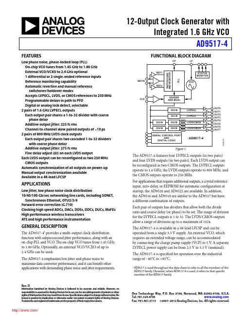
12-Output Clock Generator withIntegrated 1.6 GHz VCOAD9517-4 Rev. DInformation furnished by Analog Devices is believed to be accurate and reliable. However, noresponsibility is assumed by Analog Devices for its use, nor for any infringements of patents or other rights of third parties that may result from its use. Specifications subject to change without notice. No license is granted by implication or otherwise under any patent or patent rights of Analog Devices. T rademarks and registered trademarks are the property of their respective owners. One Technology Way, P.O. Box 9106, Norwood, M A 02062-9106, U.S.A. Tel: 781.329.4700 Fax: 781.461.3113 ©2007–2012 Analog Devices, Inc. All rights reserved.FEATURESLow phase noise, phase-locked loop (PLL)On-chip VCO tunes from 1.45 GHz to 1.80 GHzExternal VCO/VCXO to 2.4 GHz optional1 differential or2 single-ended reference inputs Reference monitoring capabilityAutomatic revertive and manual referenceswitchover/holdover modesAccepts LVPECL, LVDS, or CMOS references to 250 MHz Programmable delays in path to PFDDigital or analog lock detect, selectable2 pairs of 1.6 GHz LVPECL outputsEach output pair shares a 1-to-32 divider with coarsephase delayAdditive output jitter: 225 fs rmsChannel-to-channel skew paired outputs of <10 ps2 pairs of 800 MHz LVDS clock outputsEach output pair shares two cascaded 1-to-32 dividerswith coarse phase delayAdditive output jitter: 275 fs rmsFine delay adjust (Δt) on each LVDS outputEach LVDS output can be reconfigured as two 250 MHz CMOS outputsAutomatic synchronization of all outputs on power-up Manual output synchronization availableAvailable in a 48-lead LFCSPAPPLICATIONSLow jitter, low phase noise clock distribution10/40/100 Gb/sec networking line cards, including SONET, Synchronous Ethernet, OTU2/3/4Forward error correction (G.710)Clocking high speed ADCs, DACs, DDSs, DDCs, DUCs, MxFEs High performance wireless transceiversATE and high performance instrumentationGENERAL DESCRIPTIONThe AD9517-41 provides a multi-output clock distribution function with subpicosecond jitter performance, along with an on-chip PLL and VCO. The on-chip VCO tunes from 1.45 GHz to 1.80 GHz. Optionally, an external VCO/VCXO of up to 2.4 GHz can be used.The AD9517-4 emphasizes low jitter and phase noise to maximize data converter performance, and it can benefit other applications with demanding phase noise and jitter requirements.FUNCTIONAL BLOCK DIAGRAM6428-1Figure 1.The AD9517-4 features four LVPECL outputs (in two pairs) and four LVDS outputs (in two pairs). Each LVDS output can be reconfigured as two CMOS outputs. The LVPECL outputs operate to 1.6 GHz, the LVDS outputs operate to 800 MHz, and the CMOS outputs operate to 250 MHz.For applications that require additional outputs, a crystal reference input, zero-delay, or EEPROM for automatic configuration at startup, the AD9520 and AD9522 are available. In addition, the AD9516 and AD9518 are similar to the AD9517 but havea different combination of outputs.Each pair of outputs has dividers that allow both the divide ratio and coarse delay (or phase) to be set. The range of division for the LVPECL outputs is 1 to 32. The LVDS/CMOS outputs allow a range of divisions up to a maximum of 1024.The AD9517-4 is available in a 48-lead LFCSP and can be operated from a single 3.3 V supply. An external VCO, which requires an extended voltage range, can be accommodatedby connecting the charge pump supply (VCP) to 5 V. A separate LVPECL power supply can be from 2.5 V to 3.3 V (nominal). The AD9517-4 is specified for operation over the industrial range of −40°C to +85°C.1 AD9517 is used throughout the data sheet to refer to all the members of the AD9517 family. However, when AD9517-4 is used, it refers to that specific member of the AD9517 family.AD9517-4Rev. | Page 2 of 80TABLE OF CONTENTSFeatures..............................................................................................1 Applications.......................................................................................1 General Description.........................................................................1 Functional Block Diagram..............................................................1 Revision History...............................................................................3 Specifications.....................................................................................4 Power Supply Requirements.......................................................4 PLL Characteristics......................................................................4 Clock Inputs..................................................................................6 Clock Outputs...............................................................................6 Timing Characteristics................................................................8 Clock Output Additive Phase Noise (Distribution Only;VCO Divider Not Used)..............................................................9 Clock Output Absolute Phase Noise (Internal VCO Used)..10 Clock Output Absolute Time Jitter (Clock GenerationUsing Internal VCO)..................................................................11 Clock Output Absolute Time Jitter (Clock CleanupUsing Internal VCO)..................................................................11 Clock Output Absolute Time Jitter (Clock GenerationUsing External VCXO)..............................................................11 Clock Output Additive Time Jitter (VCO DividerNot Used).....................................................................................12 Clock Output Additive Time Jitter (VCO Divider Used).....12 Delay Block Additive Time Jitter..............................................13 Serial Control Port.....................................................................13 PD , SYNC , and RESET Pins.....................................................14 LD, STATUS, and REFMON Pins............................................14 Power Dissipation.......................................................................15 Timing Diagrams............................................................................16 Absolute Maximum Ratings..........................................................17 Thermal Resistance....................................................................17 ESD Caution................................................................................17 Pin Configuration and Function Descriptions...........................18 Typical Performance Characteristics...........................................20 Terminology....................................................................................26 Detailed Block Diagram................................................................27 Theory of Operation......................................................................28 Operational Configurations......................................................28 Digital Lock Detect (DLD).......................................................37 Clock Distribution.....................................................................41 Reset Modes................................................................................49 Power-Down Modes..................................................................50 Serial Control Port.........................................................................51 Serial Control Port Pin Descriptions.......................................51 General Operation of Serial Control Port...............................51 The Instruction Word (16 Bits)................................................52 MSB/LSB First Transfers...........................................................52 Thermal Performance....................................................................55 Control Registers............................................................................56 Control Register Map Overview..............................................56 Control Register Map Descriptions.........................................59 Applications Information..............................................................76 Frequency Planning Using the AD9517..................................76 Using the AD9517 Outputs for ADC Clock Applications....76 LVPECL Clock Distribution.....................................................77 LVDS Clock Distribution..........................................................77 CMOS Clock Distribution........................................................78 Outline Dimensions.......................................................................79 Ordering Guide.. (79)DAD9517-4Rev. D | Page 3 of 80REVISION HISTORY1/12—Rev. C to Rev. DChanges to Table 62 ........................................................................ 75 5/11—Rev. B to Rev. CChanges to Features, Applications, and General Description Sections ............................................................................................... 1 Change to CPRSET Pin Resistor Parameter, Table 1 .................... 4 Changes to Table 2 ............................................................................ 4 Changes to Table 4 ............................................................................ 6 Changes to Logic 1 Current and Logic 0 CurrentParameters, Table 15 ....................................................................... 14 Changes to Table 20 ........................................................................ 18 Change to Caption, Figure 8 .......................................................... 20 Change to Caption, Figure 15 ........................................................ 21 Change to Captions, Figure 25 and Figure 26 ............................. 23 Added Figure 41; Renumbered Sequentially ............................... 25 Changes to On-Chip VCO Section ............................................... 34 Changes to Reference Switchover Section ................................... 35 Changes to Prescaler Section and Change to Comments/Conditions Column, Table 28 ................................... 36 Changes to Automatic/Internal Holdover Mode Sectionand Frequency Status Monitors Section ....................................... 39 Changes to VCO Calibration Section ........................................... 40 Changes to Clock Distribution Section ........................................ 41 Changes to Write Section ............................................................... 51 Change to The Instruction Word (16 Bits) Section .................... 52 Change to Figure 65 ........................................................................ 53 Change to Thermal Performance Section .................................... 55 Changes to Register Address 0x01C, Bits[4:3], Table 52 ............ 56 Changes to Address 0x017, Bits[1:0] and Address 0x018,Bits[2:0], Table 54 ............................................................................ 62 Changes to Register Address 0x01C, Bits[5:1], Table 54 ............ 64 Change to LVPECL Clock Distribution Section ......................... 77 5/10—Rev. A to Rev. BChanges to Default Values of LVDS/CMOS OutputsSection in Table 52 .......................................................................... 56 Changes to Register 0x140, Bit 0; Register 0x142, Bit 0;Register 0x143, Bit 0 in Table 57 ................................................... 69 Updated Outline Dimensions, Changes to Ordering Guide ..... 78 1/10—Rev. 0 to Rev. AAdded 48-Lead LFCSP Package (CP-48-8) .................... Universal Changes to Features, Applications, and General Description ..... 1 Change to CPRSET Pin Resistor Parameter .................................. 4 Changes to Table 4 ............................................................................ 6 Changes to V CP Supply Parameter ................................................. 14 Changes to Table 19 ........................................................................ 16 Added Exposed Paddle Notation to Figure 6; Changes toTable 20 ............................................................................................. 17 Change to High Frequency Clock Distribution—CLK orExternal VCO > 1600 MHz Section; Change to Table 22 .......... 27 Changes to Table 24 ........................................................................ 29 Change to Configuration and Register Settings Section ........... 31 Change to Phase Frequency Detector (PFD) Section ................ 32 Changes to Charge Pump (CP), On-Chip VCO, PLLExternal Loop Filter, and PLL Reference Inputs Sections ......... 33 Change to Figure 46; Added Figure 47 ......................................... 33 Changes to Reference Switchover and VCXO/VCOFeedback Divider N—P , A, B, R Sections .................................... 34 Changes to Table 28 ........................................................................ 35 Change to Holdover Section .......................................................... 37 Changes to VCO Calibration Section ........................................... 39 Changes to Clock Distribution Section ........................................ 40 Change to Clock Frequency Division Section;Change to Table 34 .......................................................................... 41 Changes to Channel Dividers—LVDS/CMOS OutputsSection; Change to Table 39 ........................................................... 43 Change to Write Section ................................................................ 50 Change to MSB/LSB First Transfers ............................................. 51 Change to Figure 64 ........................................................................ 52 Added Thermal Performance Section .......................................... 54 Changes to 0x003 Register Address .............................................. 55 Changes to Table 53 ........................................................................ 58 Changes to Table 54 ........................................................................ 59 Changes to Table 55 ........................................................................ 65 Changes to Table 56 ........................................................................ 67 Changes to Table 57 ........................................................................ 69 Changes to Table 58 ........................................................................ 71 Changes to Table 59 ........................................................................ 72 Changes to Table 60 and Table 61 ................................................. 74 Added Frequency Planning Using the AD9517 Section ............ 75 Changes to Figure 70 and Figure 72; Added Figure 71 .............. 76 Changes to LVDS Clock Distribution Section ............................ 76 Added Exposed Paddle Notation to Outline Dimensions ......... 78 Changes to Ordering Guide ........................................................... 78 7/07—Revision 0: Initial VersionAD9517-4Rev. | Page 4 of 80SPECIFICATIONSTypical is given for V S = V S_LVPECL = 3.3 V ± 5%; V S ≤ V CP ≤ 5.25 V; T A = 25°C; R SET = 4.12 kΩ; CP RSET = 5.1 kΩ, unless otherwise noted. Minimum and maximum values are given over full V S and T A (−40°C to +85°C) variation.POWER SUPPLY REQUIREMENTSTable 1.Parameter Min Typ Max Unit Test Conditions/Comments V S 3.135 3.3 3.465 V 3.3 V ± 5% V S_LVPECL 2.375 V S V Nominally 2.5 V to 3.3 V ± 5% V CP V S 5.25 V Nominally 3.3 V to 5.0 V ± 5% RSET Pin Resistor 4.12 kΩ Sets internal biasing currents; connect to ground CPRSET Pin Resistor 2.7 5.1 10 kΩ Sets internal CP current range, nominally 4.8 mA (CP_lsb = 600 μA);actual current can be calculated by CP_lsb = 3.06/CPRSET; connect to groundBYPASS Pin Capacitor 220 nF Bypass for internal LDO regulator; necessary for LDO stability;connect to groundPLL CHARACTERISTICSDAD9517-4Rev. | Page 5 of 80Parameter Min Typ Max Unit Test Conditions/Comments CHARGE PUMP (CP) CP V is CP pin voltage; V CP is charge pump power supply voltage I CP Sink/Source Programmable High Value 4.8 mA With CP RSET = 5.1 kΩ Low Value 0.60 mA Absolute Accuracy 2.5 % CP V = V CP /2 V CP RSET Range 2.7/10kΩI CP High Impedance Mode Leakage 1 nA Sink-and-Source Current Matching 2 % 0.5 < CP V < V CP − 0.5 V I CP vs. CP V 1.5 % 0.5 < CP V < V CP − 0.5 V I CP vs. Temperature 2 % CP V = V CP /2 V PRESCALER (PART OF N DIVIDER) See the VCXO/VCO Feedback Divider N—P , A, B, R section Prescaler Input Frequency P = 1 FD 300 MHz P = 2 FD 600 MHz P = 3 FD 900 MHz P = 2 DM (2/3) 200 MHz P = 4 DM (4/5) 1000 MHz P = 8 DM (8/9) 2400 MHz P = 16 DM (16/17) 3000 MHz P = 32 DM (32/33) 3000 MHz Prescaler Output Frequency 300 MHz A, B counter input frequency (prescaler input frequency divided by P) PLL DIVIDER DELAYS Register 0x019: R, Bits[5:3]; N, Bits[2:0]; see Table 54 000 Off ps 001 330 ps 010 440 ps 011 550 ps 100 660 ps 101 770 ps 110 880 ps 111 990 ps NOISE CHARACTERISTICS In-Band Phase Noise of the Charge Pump/Phase Frequency Detector (In-Band Is Within the LBW of the PLL) The PLL in-band phase noise floor is estimated by measuring the in-band phase noise at the output of the VCO and subtracting 20 log(N) (where N is the value of the N divider) At 500 kHz PFD Frequency −165 dBc/Hz At 1 MHz PFD Frequency −162 dBc/Hz At 10 MHz PFD Frequency −151 dBc/Hz At 50 MHz PFD Frequency −143 dBc/Hz PLL Figure of Merit (FOM) −220 dBc/Hz Reference slew rate > 0.25 V/ns; FOM +10 log(f PFD ) is an approxi-mation of the PFD/CP in-band phase noise (in the flat region)inside the PLL loop bandwidth; when running closed-loop, the phase noise, as observed at the VCO output, is increased by 20 log(N)PLL DIGITAL LOCK DETECT WINDOW 2Signal available at LD, STATUS, and REFMON pins when selectedby appropriate register settingsRequired to Lock (Coincidence of Edges) Selected by Register 0x017[1:0] and Register 0x018[4] Low Range (ABP 1.3 ns, 2.9 ns) 3.5 ns Register 0x017[1:0] = 00b, 01b, 11b; Register 0x018[4] = 1b High Range (ABP 1.3 ns, 2.9 ns) 7.5 ns Register 0x017[1:0] = 00b, 01b, 11b; Register 0x018[4] = 0b High Range (ABP 6.0 ns) 3.5 ns Register 0x017[1:0] = 10b; Register 0x018[4] = 0bTo Unlock After Lock (Hysteresis)2Low Range (ABP 1.3 ns, 2.9 ns) 7 ns Register 0x017[1:0] = 00b, 01b, 11b; Register 0x018[4] = 1b High Range (ABP 1.3 ns, 2.9 ns) 15 ns Register 0x017[1:0] = 00b, 01b, 11b; Register 0x018[4] = 0b High Range (ABP 6.0 ns) 11 ns Register 0x017[1:0] = 10b; Register 0x018[4] = 0b1 REFIN and REFIN self-bias points are offset slightly to avoid chatter on an open input condition.2For reliable operation of the digital lock detect, the period of the PFD frequency must be greater than the unlock-after-lock time.DAD9517-4Rev. | Page 6 of 80CLOCK INPUTS1Below about 1 MHz, the input should be dc-coupled. Care should be taken to match V CM .CLOCK OUTPUTSDAD9517-4Rev. | Page 7 of 80Parameter Min Typ Max Unit Test Conditions/Comments CMOS CLOCK OUTPUTSOUT4A, OUT4B, OUT5A, OUT5B,OUT6A, OUT6B, OUT7A, OUT7BSingle-ended; termination = 10 pF Output Frequency 250 MHz See Figure 27 Output Voltage High (V OH ) V S − 0.1 V At 1 mA load Low (V OL ) 0.1 V At 1 mA load Source Current Exceeding these values can result in damage to the part Static 20 mA Dynamic 16 mA Sink Current Exceeding these values can result in damage to the part Static 8 mA Dynamic 16 mADAD9517-4Rev. | Page 8 of 80TIMING CHARACTERISTICSTable 5.Parameter Min Typ Max Unit Test Conditions/CommentsLVPECLTermination = 50 Ω to V S − 2 V; level = 810 mV Output Rise Time, t RP 70 180 ps 20% to 80%, measured differentially Output Fall Time, t FP70 180 ps 80% to 20%, measured differentially PROPAGATION DELAY, t PECL , CLK-TO-LVPECL OUTPUTHigh Frequency Clock Distribution Configuration 835 995 1180 ps See Figure 43 Clock Distribution Configuration 773 933 1090 ps See Figure 45 Variation with Temperature 0.8 ps/°C OUTPUT SKEW, LVPECL OUTPUTS 1LVPECL Outputs That Share the Same Divider 5 15 ps LVPECL Outputs on Different Dividers 13 40 ps All LVPECL Outputs Across Multiple Parts 220 psLVDSTermination = 100 Ω differential; 3.5 mA Output Rise Time, t RL 170 350 ps 20% to 80%, measured differentially 2 Output Fall Time, t FL160 350 ps 20% to 80%, measured differentially 2 PROPAGATION DELAY, t LVDS , CLK-TO-LVDS OUTPUT Delay off on all outputs For All Divide Values1.4 1.82.1 ns Variation with Temperature 1.25 ps/°COUTPUT SKEW, LVDS OUTPUTS 1Delay off on all outputs LVDS Outputs That Share the Same Divider 6 62 ps LVDS Outputs on Different Dividers 25 150 ps All LVDS Outputs Across Multiple Parts 430 psCMOSTermination = openOutput Rise Time, t RC 495 1000 ps 20% to 80%; C LOAD = 10 pF Output Fall Time, t FC475 985 ps 80% to 20%; C LOAD = 10 pF PROPAGATION DELAY, t CMOS , CLK-TO-CMOS OUTPUT Fine delay off For All Divide Values1.62.1 2.6 ns Variation with Temperature 2.6 ps/°COUTPUT SKEW, CMOS OUTPUTS 1Fine delay off CMOS Outputs That Share the Same Divider 4 66 ps All CMOS Outputs on Different Dividers 28 180 ps All CMOS Outputs Across Multiple Parts 675 psDELAY ADJUST 3LVDS and CMOSShortest Delay Range 4 Register 0x0A1 (0x0A4, 0x0A7, 0x0AA), Bits[5:0] = 101111b Zero Scale 50 315 680 ps Register 0x0A2 (0x0A5, 0x0A8, 0x0AB), Bits[5:0] = 000000b Full Scale540 880 1180 ps Register 0x0A2 (0x0A5, 0x0A8, 0x0AB), Bits[5:0] = 101111b Longest Delay Range 4 Register 0x0A1 (0x0A4, 0x0A7, 0x0AA), Bits[5:0] = 000000b Zero Scale 200 570 950 ps Register 0x0A2 (0x0A5, 0x0A8, 0x0AB), Bits[5:0] = 000000b Quarter Scale 1.72 2.31 2.89 ns Register 0x0A2 (0x0A5, 0x0A8, 0x0AB), Bits[5:0] = 001100b Full Scale5.7 8.0 10.1 ns Register 0x0A2 (0x0A5, 0x0A8, 0x0AB), Bits[5:0] = 101111b Delay Variation with Temperature Short Delay Range 5Zero Scale 0.23 ps/°C Full Scale−0.02 ps/°C Long Delay Range 5Zero Scale 0.3 ps/°C Full Scale0.24 ps/°C1 This is the difference between any two similar delay paths while operating at the same voltage and temperature. 2Corresponding CMOS drivers set to A for noninverting and B for inverting. 3The maximum delay that can be used is a little less than one-half the period of the clock. A longer delay disables the output. 4Incremental delay; does not include propagation delay. 5All delays between zero scale and full scale can be estimated by linear interpolation.DAD9517-4Rev. | Page 9 of 80CLOCK OUTPUT ADDITIVE PHASE NOISE (DISTRIBUTION ONLY; VCO DIVIDER NOT USED)Table 6.Parameter Min Typ Max Unit Test Conditions/Comments CLK-TO-LVPECL ADDITIVE PHASE NOISE Distribution section only; does not include PLL and VCO CLK = 1 GHz, Output = 1 GHz Input slew rate > 1 V/ns Divider = 1 At 10 Hz Offset −109 dBc/Hz At 100 Hz Offset −118 dBc/Hz At 1 kHz Offset −130 dBc/Hz At 10 kHz Offset −139 dBc/Hz At 100 kHz Offset −144 dBc/Hz At 1 MHz Offset −146 dBc/Hz At 10 MHz Offset −147 dBc/Hz At 100 MHz Offset −149 dBc/Hz CLK = 1 GHz, Output = 200 MHz Input slew rate > 1 V/ns Divider = 5 At 10 Hz Offset −120 dBc/Hz At 100 Hz Offset −126 dBc/Hz At 1 kHz Offset −139 dBc/Hz At 10 kHz Offset −150 dBc/Hz At 100 kHz Offset −155 dBc/Hz At 1 MHz Offset −157 dBc/Hz >10 MHz Offset −157 dBc/Hz CLK-TO-LVDS ADDITIVE PHASE NOISE Distribution section only; does not include PLL and VCO CLK = 1.6 GHz, Output = 800 MHz Input slew rate > 1 V/ns Divider = 2 At 10 Hz Offset −103 dBc/Hz At 100 Hz Offset −110 dBc/Hz At 1 kHz Offset −120 dBc/Hz At 10 kHz Offset −127 dBc/Hz At 100 kHz Offset −133 dBc/Hz At 1 MHz Offset −138 dBc/Hz At 10 MHz Offset −147 dBc/Hz At 100 MHz Offset −149 dBc/Hz CLK = 1.6 GHz, Output = 400 MHz Input slew rate > 1 V/ns Divider = 4 At 10 Hz Offset −114 dBc/Hz At 100 Hz Offset −122 dBc/Hz At 1 kHz Offset −132 dBc/Hz At 10 kHz Offset −140 dBc/Hz At 100 kHz Offset −146 dBc/Hz At 1 MHz Offset −150 dBc/Hz >10 MHz Offset −155 dBc/Hz CLK-TO-CMOS ADDITIVE PHASE NOISE Distribution section only; does not include PLL and VCO CLK = 1 GHz, Output = 250 MHz Input slew rate > 1 V/ns Divider = 4 At 10 Hz Offset −110 dBc/Hz At 100 Hz Offset −120 dBc/Hz At 1 kHz Offset −127 dBc/Hz At 10 kHz Offset −136 dBc/Hz At 100 kHz Offset −144 dBc/Hz At 1 MHz Offset −147 dBc/Hz >10 MHz Offset −154 dBc/HzDAD9517-4Rev. | Page 10 of 80Parameter Min Typ Max Unit Test Conditions/Comments CLK = 1 GHz, Output = 50 MHz Input slew rate > 1 V/ns Divider = 20 At 10 Hz Offset −124 dBc/Hz At 100 Hz Offset −134 dBc/Hz At 1 kHz Offset −142 dBc/Hz At 10 kHz Offset −151 dBc/Hz At 100 kHz Offset −157 dBc/Hz At 1 MHz Offset −160 dBc/Hz >10 MHz Offset −163 dBc/HzCLOCK OUTPUT ABSOLUTE PHASE NOISE (INTERNAL VCO USED)Table 7.Parameter Min Typ Max Unit Test Conditions/Comments LVPECL ABSOLUTE PHASE NOISE Internal VCO; direct to LVPECL output VCO = 1800 MHz; Output = 1800 MHz At 1 kHz Offset −47 dBc/Hz At 10 kHz Offset −82 dBc/Hz At 100 kHz Offset −106 dBc/Hz At 1 MHz Offset −125 dBc/Hz At 10 MHz Offset −142 dBc/Hz At 40 MHz Offset −146 dBc/Hz VCO = 1625 MHz; Output = 1625 MHz At 1 kHz Offset −55 dBc/Hz At 10 kHz Offset −85 dBc/Hz At 100 kHz Offset −109 dBc/Hz At 1 MHz Offset −128 dBc/Hz At 10 MHz Offset −143 dBc/Hz At 40 MHz Offset −147 dBc/Hz VCO = 1450 MHz; Output = 1450 MHz At 1 kHz Offset −61 dBc/Hz At 10 kHz Offset −90 dBc/Hz At 100 kHz Offset −113 dBc/Hz At 1 MHz Offset −131 dBc/Hz At 10 MHz Offset −144 dBc/Hz At 40 MHz Offset −148 dBc/HzD分销商库存信息:ANALOG-DEVICESAD9517-4ABCPZ AD9517-4ABCPZ-RL7AD9517-4A/PCBZ。
AD转换芯片介绍

l???????ADS7812?低功耗串行12位采样模数转换器
l???????ADS7810?12位800kHz采样CMOS模数转换器
l???????ADS7800?12位3us采样模数转换器
l???????ADS574??兼容微处理器的采样CMOSA/D转换器?
l???????THS1007?10位6MSPS同步采样四路通道ADC;包含并行DSP/uPI/F通道自动扫描?
l???????ADS901??10位20MSPSADC,具有单端/差动输入、外部参考和可调节全范围?
l???????ADS900??10位20MSPSADC,具有单端/差动输入、内部基准和可调节全范围?
l???????ADS822?10位40MSPSADC,具有单端/差动输入、内/外基准和断电、引脚符合ADS823/6/8?
l???????ADS821?10位40MSPSADC,单端/差动输入具有内部基准和9.3位ENOB?
l???????ADS820?10位20MSPSADC,单端/差动输入具有内部基准和9.5位ENOB?
l???????TLC3545?14位200KSPSADC,具有串行输出、自动断电和伪差动输入?
l???????TLC3544?14位、5V、200KSPS、4通道单级性ADC
l???????TLC3541?14位200KSPSADC系列输出、自动断电、单端输入?
l???????THS1403?14位、3MSPSADC单通道、差动输入、DSP/uPIF、可编程增益放大器、内部S&H?
l???????TLC4541?16位200KSPSADC,具有串行输出、自动断电和单端输入
广州致远电子 PCA9548AB AD APW IC 多路复用器和开关 产品数据手册
PCA9548AB/AD/APW2广州致远电子有限公司类别内容关键词 PCA9548A 、多路复用器、开关摘 要 PCA9548A 是一款通过I 2C 总线控制的八进制双向转换开关1. 概述PCA9548A是一款通过I2C总线控制的八进制双向转换开关。
它的每对SCL/ SDA上行通道可以扩展为八对下行通道,可以通过可编程控制寄存器的内容来选择任意单一的SCx/SDx通道或者组合通道。
由多路复用器的通门,V DD管脚可以用来限制PCA9547通过的最高电压,这使得每一对SCL/SDA都可以使用不同的总线电压,因此1.8V、2.5V或3.3V 的器件可以在无其它保护的情况下与5V的器件进行通信。
它的外部上拉电阻将总线拉高至每个通道所要求的电压电平,所有I/O管脚都可以承受5V电压。
当一次低有效的电压复位输入时,会使得PCA9548A能恢复到下行I2C总线处于低电平的状态。
就像内部上电复位的功能一样,复位引脚拉低会复位I2C总线并且禁止所有的通道。
2. 特征8路双向转换开关;I2C总线逻辑接口,兼容的SMBus标准;低电压输入复位;3地址引脚允许I2C总线连接多达8个设备;在任意组合中,可以通过I2C总线选择通道;上电时所有开关通道被禁止;低导通电阻的多路复用器;转换器允许总线电压在1.8V,2.5V,3.3V和5V的电平之间转换;上电时无干扰脉冲信号;支持热插拔;待机电流更低;电源电压运行时范围为2.3V至5.5V ;5伏宽压输入;0 Hz到400 kHz的时钟频率;ESD 保护:JESD22-A114 为2000V HBM,JESD22-A115 为200V 和JESD22-C101 为1000V CDM ;超过100mA 的JESDEC 标准JESD78 要进行栓锁测试(Latch-up testing);三种封装形式:SO24 ,TSSOP24和HVQFN24。
3. 订购信息3.1 订购信息器件的相关信息如表3.1所示:表3.1 器件的相关信息封装产品型号名称说明版本PCA9548ABS HVQFN24热增强型超薄四方扁平塑料封装;无引脚;24端子;大小为4×4×0.85mmSOT616-1PCA9548AD SO24小外形塑料封装;24个引脚;宽度为7.5mmSOT137-1PCA9548APW TSSOP24 小外形薄体收缩型塑料封装;24个引脚;宽度为4.4mmSOT355-13.2 订购选择器件选型的相关参数如表3.2所示:表3.2 器件选型参数产品型号顶层标号温度范围PCA9548ABS 548A -40 ℃ to +85 ℃PCA9548AD PCA9548AD -40 ℃ to +85 ℃PCA9548APW PCA9548A -40 ℃ to +85 ℃4. 内部结构框图PCA9548A的内部结构框图如图4.1所示:图4.1 PCA9548A的内部结构框图5. 引脚信息5.1 引脚图SO24封装形式的引脚配置如图5.1所示:图5.1 PCA9548AD引脚配置图TSSOP24封装形式的引脚配置如图5.2所示:图5.2 PCA9548APW引脚配置图HVQFN封装形式的引脚配置如图5.3所示:图5.3 PCA9548ABS引脚配置图5.2 引脚说明各个封装类型的引脚说明如表5.1所示:表5.1 引脚说明SD2 8SC2 9SD3 10续上表引脚说明标号SO,TSSOP HVQFNSD5 15 12 串行数据5SC5 16 13 串行时钟5SD6 17 14 串行数据6SC6 18 15 串行时钟6SD7 19 16 串行数据7SC7 20 17 串行时钟7A2 21 18 地址2输入SCL 22 19 串行时钟线SDA 23 20 串行数据线V DD 24 21 电源信号[1]HVQFN封装的地信号连接到V SS引脚和裸露焊盘中心。
ADE7878ACPZ;ADE7854ACPZ;ADE7854ACPZ-RL;ADE7858ACPZ-RL;ADE7868ACPZ-RL;中文规格书,Datasheet资料

Polyphase Multifunction Energy Metering ICADE7854/ADE7858/ADE7868/ADE7878 Rev. EInformation furnished by Analog Devices is believed to be accurate and reliable. However, noresponsibility is assumed by Analog Devices for its use, nor for any infringements of patents or other rights of third parties that may result from its use. Specifications subject to change without notice. No license is granted by implication or otherwise under any patent or patent rights of Analog Devices. T rademarks and registered trademarks are the property of their respective owners. One Technology Way, P.O. Box 9106, Norwood, MA 02062-9106, U.S.A. Tel: 781.329.4700 Fax: 781.461.3113 ©2010–2011 Analog Devices, Inc. All rights reserved.FEATURESHighly accurate; supports EN 50470-1, EN 50470-3,IEC 62053-21, IEC 62053-22, and IEC 62053-23 standards Compatible with 3-phase, 3- or 4-wire (delta or wye), and other 3-phase servicesSupplies total (fundamental and harmonic) active, reactive (ADE7878, ADE7868, and ADE7858 only), and apparent energy, and fundamental active/reactive energy (ADE7878 only) on each phase and on the overall systemLess than 0.1% error in active and reactive energy over a dynamic range of 1000 to 1 at T A = 25°CLess than 0.2% error in active and reactive energy over a dynamic range of 3000 to 1 at T A = 25°CSupports current transformer and di/dt current sensors Dedicated ADC channel for neutral current input (ADE7868 and ADE7878 only)Less than 0.1% error in voltage and current rms over a dynamic range of 1000 to 1 at T A = 25°CSupplies sampled waveform data on all three phases and on neutral currentSelectable no load threshold levels for total and fundamental active and reactive powers, as well as for apparent powersLow power battery mode monitors phase currents for antitampering detection (ADE7868 and ADE7878 only) Battery supply input for missing neutral operationPhase angle measurements in both current and voltage channels with a typical 0.3° errorWide-supply voltage operation: 2.4 V to 3.7 VReference: 1.2 V (drift 10 ppm/°C typical) with external overdrive capabilitySingle 3.3 V supply40-lead lead frame chip scale package (LFCSP), Pb-free Operating temperature: −40°C to +85°CFlexible I2C, SPI, and HSDC serial interfaces APPLICATIONSEnergy metering systemsGENERAL DESCRIPTIONThe ADE7854/ADE7858/ADE7868/ADE7878 are high accuracy, 3-phase electrical energy measurement ICs with serial interfaces and three flexible pulse outputs. The ADE78xx devices incorporate second-order sigma-delta (Σ-Δ) analog-to-digital converters (ADCs), a digital integrator, reference circuitry, and all of the signal processing required to perform total (fundamental and harmonic) active, reactive (ADE7878, ADE7868, and ADE7858), and apparent energy measurement and rms calcu-lations, as well as fundamental-only active and reactive energy measurement (ADE7878) and rms calculations. A fixed function digital signal processor (DSP) executes this signal processing. The DSP program is stored in the internal ROM memory. The ADE7854/ADE7858/ADE7868/ADE7878 are suitable for measuring active, reactive, and apparent energy in various 3-phase configurations, such as wye or delta services, with both three and four wires. The ADE78xx devices provide system calibration features for each phase, that is, rms offset correction, phase calibration, and gain calibration. The CF1, CF2, and CF3 logic outputs provide a wide choice of power information: total active, reactive, and apparent powers, or the sum of the current rms values, and fundamental active and reactive powers.The ADE7854/ADE7858/ADE7868/ADE7878 contain wave-form sample registers that allow access to all ADC outputs. The devices also incorporate power quality measurements, such as short duration low or high voltage detections, short duration high current variations, line voltage period measurement, and angles between phase voltages and currents. Two serial interfaces, SPI and I2C, can be used to communicate with the ADE78xx. A dedicated high speed interface, the high speed data capture (HSDC) port, can be used in conjunction with I2C to provide access to the ADC outputs and real-time power information. The ADE7854/ADE7858/ADE7868/ADE7878 also have two interrupt request pins, IRQ0 and IRQ1, to indicate that an enabled interrupt event has occurred. For the ADE7868/ADE7878, three specially designed low power modes ensure the continuity of energy accumulation when the ADE7868/ADE7878 is in a tam-pering situation. See for a quick reference chart listing each part and its functions. The ADE78xx are available in the 40-lead LFCSP, Pb-free package.Table 1Table 1. Part ComparisonPart No. WATT VARIRMS,VRMS,andVA di/dtFundamentalWATT andVARTamperDetectand LowPowerModes ADE7878 Yes Yes Yes Yes Yes Yes ADE7868 Yes Yes Yes Yes No Yes ADE7858 Yes Yes Yes Yes No No ADE7854 Yes No Yes Yes No NoADE7854/ADE7858/ADE7868/ADE7878Rev. E | Page 2 of 96TABLE OF CONTENTSFeatures..............................................................................................1 Applications.......................................................................................1 General Description.........................................................................1 Revision History...............................................................................3 Functional Block Diagrams.............................................................4 Specifications.....................................................................................8 Timing Characteristics..............................................................11 Absolute Maximum Ratings..........................................................14 Thermal Resistance....................................................................14 ESD Caution................................................................................14 Pin Configuration and Function Descriptions...........................15 Typical Performance Characteristics...........................................17 Test Circuit......................................................................................19 Terminology....................................................................................20 Power Management........................................................................21 PSM0—Normal Power Mode (All Parts)................................21 PSM1—Reduced Power Mode (ADE7868, ADE7878 Only)21 PSM2—Low Power Mode (ADE7868, ADE7878 Only).......21 PSM3—Sleep Mode (All Parts)................................................22 Power-Up Procedure..................................................................24 Hardware Reset...........................................................................25 Software Reset Functionality....................................................25 Theory of Operation......................................................................26 Analog Inputs..............................................................................26 Analog-to-Digital Conversion..................................................26 Current Channel ADC...............................................................27 di/dt Current Sensor and Digital Integrator..............................29 Voltage Channel ADC...............................................................30 Changing Phase Voltage Datapath...........................................31 Power Quality Measurements...................................................32 Phase Compensation.................................................................37 Reference Circuit........................................................................39 Digital Signal Processor.............................................................39 Root Mean Square Measurement.............................................40 Active Power Calculation..........................................................44 Reactive Power Calculation—ADE7858, ADE7868, ADE7878 Only..............................................................................................49 Apparent Power Calculation.....................................................54 Waveform Sampling Mode.......................................................57 Energy-to-Frequency Conversion............................................57 No Load Condition....................................................................61 Checksum Register.....................................................................63 Interrupts.....................................................................................64 Serial Interfaces..........................................................................65 ADE7878 Evaluation Board......................................................72 Die Version..................................................................................72 Silicon Anomaly.............................................................................73 ADE7854/ADE7858/ADE7868/ADE7878 FunctionalityIssues............................................................................................73 Functionality Issues....................................................................73 Section 1. ADE7854/ADE7858/ADE7868/ADE7878Functionality Issues....................................................................74 Registers List...................................................................................75 Outline Dimensions.......................................................................93 Ordering Guide.. (93)ADE7854/ADE7858/ADE7868/ADE7878Rev. E | Page 3 of 96REVISION HISTORY4/11—Rev. D to Rev. EChanges to Input Clock FrequencyParameter, Table 2..............10 Changes to Current RMS Offset Compensation Section..........42 Changes to Voltage RMS Offset Compensation Section...........44 Changes to Note 2, Table 30...........................................................77 Changes to Address 0xE707, Table 33..........................................80 Changes to Table 45........................................................................87 Changes to Table 46........................................................................88 Changes to Bit Location 7:3, Default Value, Table 54.. (92)2/11—Rev. C to Rev. DChanges to Figure 1...........................................................................4 Changes to Figure 2...........................................................................5 Changes to Figure 3...........................................................................6 Changes to Figure 4...........................................................................7 Changes to Table 2............................................................................8 Changed SCLK Edge to HSCLK Edge, Table 5...........................13 Change to Current Channel HPF Section...................................28 Change to di/dt Current Sensor and Digital IntegratorSection..............................................................................................30 Changes to Digital Signal Processor Section...............................39 Changes to Figure 59......................................................................44 Changes to Figure 62......................................................................47 Changes to Figure 65......................................................................49 Changes to Figure 66......................................................................52 Changes to Line Cycle Reactive Energy Accumulation Mode Section and to Figure 67.................................................................53 No Load Detection Based On Total Active, Reactive Powers Section..............................................................................................61 Change to Equation 50...................................................................63 Changes to the HSDC Interface Section......................................70 Changes to Figure 87 and Figure 88.............................................71 Changes to Figure 89......................................................................72 Changes to Table 30 (77)11/10—Rev. B to Rev. CChange to Signal-to-Noise-and-Distortion Ratio, SINADParameter, Table 1.............................................................................9 Changes to Figure 18......................................................................18 Changes to Figure 22......................................................................19 Changes to Silicon Anomaly Section............................................72 Added Table 28 to Silicon Anomaly Section, RenumberedTables Sequentially..........................................................................73 8/10—Rev. A to Rev. BChanges to Figure 1..........................................................................4 Changes to Figure 2..........................................................................5 Changes to Figure 3..........................................................................6 Changes to Figure 4..........................................................................7 Change to Table 8............................................................................16 Changes to Power-Up Procedure Section....................................23 Changes to Equation 6 and Equation 7........................................33 Changes to Equation 17.................................................................43 Changes to Active Power Offset Calibration Section.................45 Changes to Figure 63......................................................................46 Changes to Reactive Power Offset Calibration Section.............49 Changes to Figure 82......................................................................65 Added Silicon Anomaly Section, Renumbered TablesSequentially (71)3/10—Rev. 0 to Rev. AAdded ADE7854, ADE7858, and ADE7878..................Universal Reorganized Layout...........................................................Universal Added Table 1, Renumbered Sequentially.....................................1 Added Figure 1, Renumbered Sequentially...................................3 Added Figure 2..................................................................................4 Added Figure 3..................................................................................5 Changes to Specifications Section..................................................7 Changes to Figure 9........................................................................14 Changes to Table 8..........................................................................14 Changes to Typical Performance Characteristics Section.........16 Changes to Figure 22......................................................................18 Changes to the Power Management Section...............................20 Changes to the Theory of Operation Section..............................25 Changes to Figure 31 and Figure 32.............................................27 Change to Equation 28...................................................................47 Changes to Figure 83......................................................................66 Changes to Figure 86......................................................................68 Changes to the Registers List Section...........................................72 Changes to Ordering Guide.. (91)2/10—Revision 0: Initial VersionADE7854/ADE7858/ADE7868/ADE7878Rev. E | Page 4 of 96FUNCTIONAL BLOCK DIAGRAMSR E S E TR E F C L K I C L K O U I A I A V A I B I B V B I C I C V C V S C L K/S C LS D AH S DA08510-204Figure 1. ADE7854 Functional Block DiagramADE7854/ADE7858/ADE7868/ADE7878Rev. E | Page 5 of 96R E S E TR E F C L K I C L K O U I A I A V A I B I B V B I C I C V C V S C L K/S C LS D AH S DA08510-203Figure 2. ADE7858 Functional Block DiagramADE7854/ADE7858/ADE7868/ADE7878Rev. E | Page 6 of 96R E S E TR E F C L K I C L K O U I A I A V A I B I B V B I C I C V C V S C L K/S C LS D AH S DAI N I N 08510-202Figure 3. ADE7868 Functional Block DiagramADE7854/ADE7858/ADE7868/ADE7878Rev. E | Page 7 of 96R E S E TR E F C L K I C L K O U I A I A V A I B I B V B I C I C V C V S C L K/S C LS D AH S DAI N I N 08510-201Figure 4. ADE7878 Functional Block DiagramADE7854/ADE7858/ADE7868/ADE7878Rev. E | Page 8 of 96SPECIFICATIONSVDD = 3.3 V ± 10%, AGND = DGND = 0 V , on-chip reference, CLKIN = 16.384 MHz, T MIN to T MAX = −40°C to +85°C. Table 2.Parameter 1, 2 Min Typ Max Unit Test Conditions/Comments ACCURACYActive Energy MeasurementActive Energy Measurement Error (per Phase)Total Active Power0.1%Over a dynamic range of 1000 to 1, PGA = 1, 2, 4; integrator off0.2 % Over a dynamic range of 3000 to 1, PGA = 1, 2, 4;integrator off0.1 % Over a dynamic range of 500 to 1, PGA = 8, 16;integrator onFundamental Active Power (ADE7878 Only) 0.1% Over a dynamic range of 1000 to 1, PGA = 1, 2, 4; integrator off 0.2 % Over a dynamic range of 3000 to 1, PGA = 1, 2, 4;integrator off0.1 % Over a dynamic range of 500 to 1, PGA = 8, 16;integrator onPhase Error Between Channels Line frequency = 45 Hz to 65 Hz, HPF on Power Factor (PF) = 0.8 Capacitive ±0.05 Degrees Phase lead 37° PF = 0.5 Inductive ±0.05 Degrees Phase lag 60° AC Power Supply Rejection VDD = 3.3 V + 120 mV rms/120 Hz, IPx = VPx =±100 mV rmsOutput Frequency Variation 0.01 % DC Power Supply Rejection VDD = 3.3 V ± 330 mV dc Output Frequency Variation 0.01 %Total Active Energy MeasurementBandwidth2 kHz REACTIVE ENERGY MEASUREMENT(ADE7858, ADE7868, AND ADE7878)Reactive Energy Measurement Error(per Phase)Total Active Power 0.1 % Over a dynamic range of 1000 to 1, PGA = 1, 2, 4;integrator off0.2 % Over a dynamic range of 3000 to 1, PGA = 1, 2, 4;integrator off0.1 % Over a dynamic range of 500 to 1, PGA = 8, 16;integrator onFundamental Active Power (ADE7878 Only) 0.1% Over a dynamic range of 1000 to 1, PGA = 1, 2, 4; integrator off 0.2 % Over a dynamic range of 3000 to 1, PGA = 1, 2, 4;integrator off0.1 % Over a dynamic range of 500 to 1, PGA = 8, 16;integrator onPhase Error Between Channels Line frequency = 45 Hz to 65 Hz, HPF on PF = 0.8 Capacitive ±0.05 Degrees Phase lead 37° PF = 0.5 Inductive ±0.05 Degrees Phase lag 60° AC Power Supply Rejection VDD = 3.3 V + 120 mV rms/120 Hz, IPx = VPx =±100 mV rmsOutput Frequency Variation 0.01 %ADE7854/ADE7858/ADE7868/ADE7878Rev. E | Page 9 of 96Parameter 1, 2Min Typ Max Unit Test Conditions/Comments DC Power Supply Rejection VDD = 3.3 V ± 330 mV dc Output Frequency Variation0.01% Total Reactive Energy Measurement Bandwidth2kHzRMS MEASUREMENTSI rms and V rms Measurement Bandwidth2 kHz I rms and V rms Measurement Error (PSM0 Mode)0.1 % Over a dynamic range of 1000 to 1, PGA = 1 MEAN ABSOLUTE VALUE (MAV)MEASUREMENT (ADE7868 AND ADE7878)I mav Measurement Bandwidth (PSM1 Mode)260 Hz I mav Measurement Error (PSM1 Mode) 0.5 % Over a dynamic range of 100 to 1, PGA = 1, 2, 4, 8 ANALOG INPUTSMaximum Signal Levels±500mV peakDifferential inputs between the following pins: IAP and IAN, IBP and IBN, ICP and ICN; single-ended inputs between the following pins: VAP and VN, VBP and VN, VCP and VN Input Impedance (DC)IAP , IAN, IBP , IBN, ICP , ICN, VAP , VBP , and VCP Pins 400 kΩVN Pin130 kΩADC Offset Error±2 mV PGA = 1, uncalibrated error, see the Terminology sectionGain Error±4 % External 1.2 V referenceWAVEFORM SAMPLINGSampling CLKIN/2048, 16.384 MHz/2048 = 8 kSPS Current and Voltage Channels See the Waveform Sampling Mode section Signal-to-Noise Ratio, SNR70 dB PGA = 1 Signal-to-Noise-and-Distortion Ratio, SINAD60 dB PGA = 1Bandwidth (−3 dB)2 kHz TIME INTERVAL BETWEEN PHASESMeasurement Error0.3 Degrees Line frequency = 45 Hz to 65 Hz, HPF on CF1, CF2, CF3 PULSE OUTPUTSMaximum Output Frequency 8 kHz WTHR = VARTHR = VATHR = PMAX = 33,516,139 Duty Cycle50%If CF1, CF2, or CF3 frequency > 6.25 Hz and CFDEN is even and > 1(1 + 1/CFDEN) × 50% If CF1, CF2, or CF3 frequency > 6.25 Hz andCFDEN is odd and > 1Active Low Pulse Width 80 ms If CF1, CF2, or CF3 frequency < 6.25 Hz Jitter 0.04 % For CF1, CF2, or CF3 frequency = 1 Hz andnominal phase currents are larger than 10% of full scaleREFERENCE INPUT REF IN/OUT Input Voltage Range 1.1 1.3 V Minimum = 1.2 V − 8%; maximum = 1.2 V + 8% Input Capacitance 10 pF ON-CHIP REFERENCE Nominal 1.207 V at the REF IN/OUT pin at T A = 25°C PSM0 and PSM1 Modes Reference Error ±2 mV Output Impedance 1.2 kΩ Temperature Coefficient 10 50 ppm/°C Maximum value across full temperature rangeof −40°C to +85°CADE7854/ADE7858/ADE7868/ADE78781 See the Typical Performance Characteristics section.2 See the Terminology section for a definition of the parameters.Rev. E | Page 10 of 96分销商库存信息:ANALOG-DEVICESADE7878ACPZ ADE7854ACPZ ADE7854ACPZ-RL ADE7858ACPZ-RL ADE7868ACPZ-RL ADE7878ACPZ-RL ADE7858ACPZ ADE7868ACPZ EVAL-ADE7878EBZ。
AD9514BCPZ;AD9514PCBZ;中文规格书,Datasheet资料
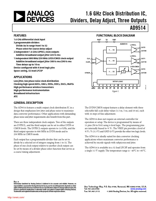
1.6 GHz Clock Distribution IC,Dividers, Delay Adjust, Three OutputsAD9514 Rev. 0Information furnished by Analog Devices is believed to be accurate and reliable. However, noresponsibility is assumed by Analog Devices for its use, nor for any infringements of patents or other rights of third parties that may result from its use. Specifications subject to change without notice. No license is granted by implication or otherwise under any patent or patent rights of Analog Devices. T rademarks and registered trademarks are the property of their respective owners. One Technology Way, P.O. Box 9106, Norwood, M A 02062-9106, U.S.A. Tel: 781.329.4700 Fax: 781.461.3113 © 2005 Analog Devices, Inc. All rights reserved.FEATURES1.6 GHz differential clock input3 programmable dividersDivide-by in range from1 to 32Phase select for coarse delay adjust2 independent 1.6 GHz LVPECL clock outputsAdditive broadband output jitter 225 fs rms1 independent 800 MHz/250 MHz LVDS/CMOS clock output Additive broadband output jitter 300 fs rms/290 fs rms Time delays up to 10 nsDevice configured with 4-level logic pinsSpace-saving, 32-lead LFCSPAPPLICATIONSLow jitter, low phase noise clock distributionClocking high speed ADCs, DACs, DDSs, DDCs, DUCs, MxFEs High performance wireless transceiversHigh performance instrumentationBroadband infrastructureATEFUNCTIONAL BLOCK DIAGRAMOUT0CLKCLKBSYNCBOUT0BOUT1OUT1BOUT2OUT2B5596-1Figure 1.GENERAL DESCRIPTIONThe AD9514 features a multi-output clock distribution IC in a design that emphasizes low jitter and phase noise to maximize data converter performance. Other applications with demanding phase noise and jitter requirements also benefit from this part. There are three independent clock outputs. Two of the outputs are LVPECL, and the third output can be set to either LVDS or CMOS levels. The LVPECL outputs operate to 1.6 GHz, and the third output operates to 800 MHz in LVDS mode and to250 MHz in CMOS mode.Each output has a programmable divider that can be set to divide by a selected set of integers ranging from 1 to 32. The phase of one clock output relative to another clock output can be set by means of a divider phase select function that serves as a coarse timing adjustment. The LVDS/CMOS output features a delay element with three selectable full-scale delay values (1.5 ns, 5 ns, and 10 ns), each with 16 steps of fine adjustment.The AD9514 does not require an external controller for operation or setup. The device is programmed by means of11 pins (S0 to S10) using 4-level logic. The programming pins are internally biased to ⅓ V S. The VREF pin provides a level of ⅔ V S. V S (3.3 V) and GND (0 V) provide the other two logic levels.The AD9514 is ideally suited for data converter clocking applications where maximum converter performance is achieved by encode signals with subpicosecond jitter.The AD9514 is available in a 32-lead LFCSP and operates from a single 3.3 V supply. The temperature range is −40°C to +85°C.AD9514Rev. 0 | Page 2 of 28TABLE OF CONTENTS Features..............................................................................................1 Applications.......................................................................................1 Functional Block Diagram..............................................................1 General Description.........................................................................1 Revision History...............................................................................2 Specifications.....................................................................................3 Clock Input....................................................................................3 Clock Outputs...............................................................................3 Timing Characteristics................................................................4 Clock Output Phase Noise..........................................................5 Clock Output Additive Time Jitter.............................................8 SYNCB, VREF, and Setup Pins.................................................10 Power............................................................................................10 Timing Diagrams............................................................................11 Absolute Maximum Ratings..........................................................12 Thermal Characteristics............................................................12 ESD Caution................................................................................12 Pin Configuration and Function Descriptions...........................13 Terminology....................................................................................14 Typical Performance Characteristics...........................................15 Functional Description..................................................................18 Overall..........................................................................................18 CLK, CLKB—Differential Clock Input.. (18)Synchronization (18)Power-On SYNC (18)SYNCB (18)R SET Resistor (19)VREF (19)Setup Configuration (19)Divider Phase Offset (22)Delay Block (22)Outputs (23)Power Supply (23)Exposed Metal Paddle (24)Power Management (24)Applications (25)Using the AD9514 Outputs for ADC Clock Applications (25)LVPECL Clock Distribution (25)LVDS Clock Distribution (26)CMOS Clock Distribution (26)Setup Pins (S0 to S10) (26)Power and Grounding Considerations and Power SupplyRejection (26)Phase Noise and Jitter Measurement Setups (27)Outline Dimensions (28)Ordering Guide (28)REVISION HISTORY7/05—Revision 0: Initial VersionAD9514Rev. 0 | Page 3 of 28SPECIFICATIONSTypical (typ) is given for V S = 3.3 V ± 5%, T A = 25°C, R SET = 4.12 kΩ, LVPECL V OD = 790 mV , unless otherwise noted. Minimum (min)and maximum (max) values are given over full V S and T A (−40°C to +85°C) variation.CLOCK INPUT Table 1.ParameterMin Typ Max Unit Test Conditions/Comments CLOCK INPUT (CLK)Input Frequency 10 1.6 GHz Input Sensitivity 1150 mV p-p Input Common-Mode Voltage, V CM1.5 1.6 1.7 V Self-biased; enables ac coupling Input Common-Mode Range, V CMR1.3 1.8 V With 200 mV p-p signal applied; dc-coupled Input Sensitivity, Single-Ended150 mV p-p CLK ac-coupled; CLKB ac-bypassed to RF ground Input Resistance4.0 4.85.6 kΩ Self-biased Input Capacitance2 pF1 A slew rate of 1 V/ns is required to meet jitter, phase noise, and propagation delay specifications.CLOCK OUTPUTS Table 2.Parameter Min Typ Max Unit Test Conditions/CommentsLVPECL CLOCK OUTPUTS Termination = 50 Ω to V S − 2 V(OUT0, OUT1) DifferentialOutput Frequency 0 1.6 GHzOutput High Voltage (V OH ) V S − 1.1 V S − 0.96 V S − 0.82 VOutput Low Voltage (V OL ) V S − 1.90 V S − 1.76 V S − 1.52 VOutput Differential Voltage (V OD ) 640 790 960 mVLVDS CLOCK OUTPUT Termination = 100 Ω differential(OUT2) DifferentialOutput Frequency 0 800 MHzDifferential Output Voltage (V OD ) 250 350 450 mVDelta V OD 30 mVOutput Offset Voltage (V OS ) 1.125 1.23 1.375 VDelta V OS 25 mVShort-Circuit Current (I SA , I SB ) 14 24 mA Output shorted to GNDCMOS CLOCK OUTPUT Single-ended measurements; termination open(OUT2) Single-Ended Complementary output on (OUT2B)Output Frequency 0 250 MHz With 5 pF loadOutput Voltage High (V OH ) V S − 0.1 V @ 1 mA loadOutput Voltage Low (V OL ) 0.1 V @ 1 mA loadAD9514Rev. 0 | Page 4 of 28TIMING CHARACTERISTICSCLK input slew rate = 1 V/ns or greater. Table 3.ParameterMin Typ Max Unit Test Conditions/Comments LVPECLTermination = 50 Ω to V S − 2 V Output Rise Time, t RP60 100 ps 20% to 80%, measured differentially Output Fall Time, t FP60 100 ps 80% to 20%, measured differentially PROPAGATION DELAY, t PECL , CLK-TO-LVPECL OUTDivide = 1355 480 635 ps Divide = 2 − 32395 530 710 ps Variation with Temperature0.5 ps/°C OUTPUT SKEW, LVPECLOUT0 to OUT1 on Same Part, t SKP 1−50 0 +55 ps Both LVPECL Outputs Across Multiple Parts, t SKP_AB 2125 ps Same LVPECL Output Across Multiple Parts, t SKP_AB 2125 ps LVDSTermination = 100 Ω differential, 3.5 mA Output Rise Time, t RL200 350 ps 20% to 80%, measured differentially Output Fall Time, t FL210 350 ps 80% to 20%, measured differentially PROPAGATION DELAY, t LVDS , CLK-TO-LVDS OUTOptional delay off Divide = 11.00 1.25 1.55 ns Divide = 2 − 321.05 1.30 1.60 ns Variation with Temperature0.9 ps/°C OUTPUT SKEW, LVDSOptional delay off LVDS Output Across Multiple Parts, t SKV_AB 2230 ps CMOSB outputs are inverted; termination = open Output Rise Time, t RC650 865 ps 20% to 80%; C LOAD = 3 pF single-ended Output Fall Time, t FC650 990 ps 80% to 20%; C LOAD = 3 pF single-ended PROPAGATION DELAY, t CMOS , CLK-TO-CMOS OUTOptional delay off Divide = 11.10 1.45 1.75 ns Divide = 2 − 321.15 1.50 1.80 ns Variation with Temperature1 ps/°C OUTPUT SKEW, CMOSOptional delay off CMOS Output Across Multiple Parts, t SKC_AB 2300 ps LVPECL-TO-LVDS OUTOutput Delay, t SKV_C560 790 950 ps LVPECL-TO-CMOS OUTOutput Delay, t SKV_C700 970 1150 ps DELAY ADJUST (OUT2; LVDS and CMOS)S0 = 1/3Zero Scale Delay Time 30.34 ns Zero Scale Variation with Temperature0.20 ps/°C Full Scale Time Delay 31.7 ns Full Scale Variation with Temperature−0.38 ps/°C S0 = 2/3Zero Scale Delay Time 30.45 ns Zero Scale Variation with Temperature0.31 ps/°C Full Scale Time Delay 35.9 ns Full Scale Variation with Temperature−1.3 ps/°CAD9514 Rev. 0 | Page 5 of 28Parameter Min Typ MaxUnit Test Conditions/Comments S0 = 1Zero Scale Delay Time 3 0.56ns Zero Scale Variation with Temperature 0.47ps/°C Full Scale Time Delay 3 11.4ns Full Scale Variation with Temperature −5ps/°C Linearity, DNL 0.2LSB Linearity, INL0.2 LSB1This is the difference between any two similar delay paths within a single device operating at the same voltage and temperature. 2 This is the difference between any two similar delay paths across multiple devices operating at the same voltage and temperature.3 Incremental delay; does not include propagation delay.CLOCK OUTPUT PHASE NOISECLK input slew rate = 1 V/ns or greater. Table 4.Parameter M in Typ M ax Unit Test Conditions/Comments CLK-TO-LVPECL ADDITIVE PHASE NOISECLK = 622.08 MHz, OUT = 622.08 MHzDivide = 1@ 10 Hz Offset −125 dBc/Hz@ 100 Hz Offset −132 dBc/Hz@ 1 kHz Offset −140 dBc/Hz@ 10 kHz Offset −148 dBc/Hz@ 100 kHz Offset −153 dBc/Hz>1 MHz Offset −154 dBc/HzCLK = 622.08 MHz, OUT = 155.52 MHzDivide = 4@ 10 Hz Offset −128 dBc/Hz@ 100 Hz Offset −140 dBc/Hz@ 1 kHz Offset −148 dBc/Hz@ 10 kHz Offset −155 dBc/Hz@ 100 kHz Offset −161 dBc/Hz>1 MHz Offset −161 dBc/HzCLK = 622.08 MHz, OUT = 38.88 MHzDivide = 16@ 10 Hz Offset −135 dBc/Hz@ 100 Hz Offset −145 dBc/Hz@ 1 kHz Offset −158 dBc/Hz@ 10 kHz Offset −165 dBc/Hz@ 100 kHz Offset −165 dBc/Hz>1 MHz Offset −166 dBc/HzCLK = 491.52 MHz, OUT = 61.44 MHzDivide = 8@ 10 Hz Offset −131 dBc/Hz@ 100 Hz Offset −142 dBc/Hz@ 1 kHz Offset −153 dBc/Hz@ 10 kHz Offset −160 dBc/Hz@ 100 kHz Offset −165 dBc/Hz>1 MHz Offset −165 dBc/HzAD9514Rev. 0 | Page 6 of 28Parameter M in Typ M ax Unit Test Conditions/Comments CLK = 491.52 MHz, OUT = 245.76 MHzDivide = 2@ 10 Hz Offset −125 dBc/Hz@ 100 Hz Offset −132 dBc/Hz@ 1 kHz Offset −140 dBc/Hz@ 10 kHz Offset −151 dBc/Hz@ 100 kHz Offset −157 dBc/Hz>1 MHz Offset −158 dBc/HzCLK = 245.76 MHz, OUT = 61.44 MHzDivide = 4@ 10 Hz Offset −138 dBc/Hz@ 100 Hz Offset −144 dBc/Hz@ 1 kHz Offset −154 dBc/Hz@ 10 kHz Offset −163 dBc/Hz@ 100 kHz Offset −164 dBc/Hz>1 MHz Offset −165 dBc/HzCLK-TO-LVDS ADDITIVE PHASE NOISECLK = 622.08 MHz, OUT= 622.08 MHzDivide = 1@ 10 Hz Offset −100 dBc/Hz@ 100 Hz Offset −110 dBc/Hz@ 1 kHz Offset −118 dBc/Hz@ 10 kHz Offset −129 dBc/Hz@ 100 kHz Offset −135 dBc/Hz@ 1 MHz Offset −140 dBc/Hz>10 MHz Offset −148 dBc/HzCLK = 622.08 MHz, OUT = 155.52 MHzDivide = 4@ 10 Hz Offset −112 dBc/Hz@ 100 Hz Offset −122 dBc/Hz@ 1 kHz Offset −132 dBc/Hz@ 10 kHz Offset −142 dBc/Hz@ 100 kHz Offset −148 dBc/Hz@ 1 MHz Offset −152 dBc/Hz>10 MHz Offset −155 dBc/HzCLK = 491.52 MHz, OUT = 245.76 MHzDivide = 2@ 10 Hz Offset −108 dBc/Hz@ 100 Hz Offset −118 dBc/Hz@ 1 kHz Offset −128 dBc/Hz@ 10 kHz Offset −138 dBc/Hz@ 100 kHz Offset −145 dBc/Hz@ 1 MHz Offset −148 dBc/Hz>10 MHz Offset −154 dBc/HzAD9514 Rev. 0 | Page 7 of 28Parameter M in Typ M ax Unit Test Conditions/Comments CLK = 491.52 MHz, OUT = 122.88 MHzDivide = 4@ 10 Hz Offset −118 dBc/Hz@ 100 Hz Offset −129 dBc/Hz@ 1 kHz Offset −136 dBc/Hz@ 10 kHz Offset −147 dBc/Hz@ 100 kHz Offset −153 dBc/Hz@ 1 MHz Offset −156 dBc/Hz>10 MHz Offset −158 dBc/HzCLK = 245.76 MHz, OUT = 245.76 MHzDivide = 1@ 10 Hz Offset −108 dBc/Hz@ 100 Hz Offset −118 dBc/Hz@ 1 kHz Offset −128 dBc/Hz@ 10 kHz Offset −138 dBc/Hz@ 100 kHz Offset −145 dBc/Hz@ 1 MHz Offset −148 dBc/Hz>10 MHz Offset −155 dBc/HzCLK = 245.76 MHz, OUT = 122.88 MHzDivide = 2@ 10 Hz Offset −118 dBc/Hz@ 100 Hz Offset −127 dBc/Hz@ 1 kHz Offset −137 dBc/Hz@ 10 kHz Offset −147 dBc/Hz@ 100 kHz Offset −154 dBc/Hz@ 1 MHz Offset −156 dBc/Hz>10 MHz Offset −158 dBc/HzCLK-TO-CMOS ADDITIVE PHASE NOISECLK = 245.76 MHz, OUT = 245.76 MHzDivide = 1@ 10 Hz Offset −110 dBc/Hz@ 100 Hz Offset −121 dBc/Hz@ 1 kHz Offset −130 dBc/Hz@ 10 kHz Offset −140 dBc/Hz@ 100 kHz Offset −145 dBc/Hz@ 1 MHz Offset −149 dBc/Hz>10 MHz Offset −156 dBc/HzCLK = 245.76 MHz, OUT = 61.44 MHzDivide = 4@ 10 Hz Offset −125 dBc/Hz@ 100 Hz Offset −132 dBc/Hz@ 1 kHz Offset −143 dBc/Hz@ 10 kHz Offset −152 dBc/Hz@ 100 kHz Offset −158 dBc/Hz@ 1 MHz Offset −160 dBc/Hz>10 MHz Offset −162 dBc/HzAD9514Rev. 0 | Page 8 of 28Parameter M in Typ M ax Unit Test Conditions/Comments CLK = 78.6432 MHz, OUT = 78.6432 MHzDivide = 1@ 10 Hz Offset −122 dBc/Hz@ 100 Hz Offset −132 dBc/Hz@ 1 kHz Offset −140 dBc/Hz@ 10 kHz Offset −150 dBc/Hz@ 100 kHz Offset −155 dBc/Hz@ 1 MHz Offset −158 dBc/Hz>10 MHz Offset −160 dBc/HzCLK = 78.6432 MHz, OUT = 39.3216 MHzDivide = 2@ 10 Hz Offset −128 dBc/Hz@ 100 Hz Offset −136 dBc/Hz@ 1 kHz Offset −146 dBc/Hz@ 10 kHz Offset −155 dBc/Hz@ 100 kHz Offset −161 dBc/Hz>1 MHz Offset −162 dBc/HzCLOCK OUTPUT ADDITIVE TIME JITTER Table 5.Parameter M in Typ M ax Unit Test Conditions/CommentsLVPECL OUTPUT ADDITIVE TIME JITTERCLK = 622.08 MHz 40 fs rms BW = 12 kHz − 20 MHzLVPECL (OUT0 and OUT1) = 622.08 MHz OUT2 offDivide = 1CLK = 622.08 MHz 55 fs rms BW = 12 kHz − 20 MHzLVPECL (OUT0 and OUT1) = 155.52 MHz OUT2 offDivide = 4CLK = 400 MHz 215 fs rms Calculated from SNR of ADC method;LVPECL (OUT0 and OUT1) = 100 MHz OUT2 offDivide = 4CLK = 400 MHz 215 fs rms Calculated from SNR of ADC method;LVPECL (OUT0, OUT1) = 100 MHz Other LVPECL and OUT2 LVDS at same frequencyDivide = 4CLK = 400 MHz 225 fs rms Calculated from SNR of ADC method;LVPECL (OUT0 or OUT1) = 100 MHzDivide = 4Other LVPECL = 50 MHz InterfererLVDS (OUT2) = 50 MHz InterfererCLK = 400 MHz 230 fs rms Calculated from SNR of ADC method;LVPECL (OUT0 or OUT1) = 100 MHzDivide = 4Other LVPECL = 50 MHz InterfererCMOS (OUT2) = 50 MHz InterfererLVDS OUTPUT ADDITIVE TIME JITTER Delay offCLK = 400 MHz 300 fs rms Calculated from SNR of ADC method;LVDS (OUT2) = 100 MHz OUT0 at same frequency; OUT1 offDivide = 4AD9514 Rev. 0 | Page 9 of 28Parameter M in Typ M ax Unit Test Conditions/Comments CLK = 400 MHz 350 fs rms Calculated from SNR of ADC methodLVDS (OUT2) = 100 MHzDivide = 4Both LVPECL = 50 MHz Interferer(s)CMOS OUTPUT ADDITIVE TIME JITTER Delay offCLK = 400 MHz 290 fs rms Calculated from SNR of ADC methodCMOS (OUT2) = 100 MHz OUT0 at same frequency; OUT1 offDivide = 4CLK = 400 MHz 315 fs rms Calculated from SNR of ADC methodCMOS (OUT2) = 100 MHzDivide = 4Both LVPECL = 50 MHz Interferer(s)DELAY BLOCK ADDITIVE TIME JITTER 1 100 MHz output; incremental additive jitterDelay FS = 1.5 ns Fine Adj. 00000 0.71 ps rmsDelay FS = 1.5 ns Fine Adj. 11111 1.2 ps rmsDelay FS = 5 ns Fine Adj. 00000 1.3 ps rmsDelay FS = 5 ns Fine Adj. 11111 2.7 ps rmsDelay FS = 10 ns Fine Adj. 00000 2.0 ps rmsDelay FS = 10 ns Fine Adj. 11111 2.8 ps rms1 This value is incremental. That is, it is in addition to the jitter of the LVDS or CMOS output without the delay. To estimate the total jitter, the LVDS or CMOS output jitter should be added to this value using the root sum of the squares (RSS) method.AD9514Rev. 0 | Page 10 of 28SYNCB, VREF, AND SETUP PINS Table 6.Parameter Min Typ Max Unit Test Conditions/CommentsSYNCBLogic High 2.7 VLogic Low 0.40 VCapacitance 2 pFVREFOutput Voltage 0.62 V S 0.76 V S V Minimum − maximum from 0 mA to 1 mA load S0 TO S10Levels0 0.1 V S V1/3 0.2 V S 0.45 V S V2/3 0.55 V S 0.8 V S V1 0.9 V S VPOWER Table 7.ParameterMin Typ Max Unit Test Conditions/Comments POWER-ON SYNCHRONIZATION 135 ms See Figure 24. V S Transit Time from 2.2 V to 3.1 VPOWER DISSIPATION 295 405 550 mW All outputs on. 2 LVPECL (divide = 2), 1 LVDS (divide = 2). No clock.Does not include power dissipated in external resistors.380 490 635 mW All outputs on. 2 LVPECL (divide = 2), 1 CMOS (divide = 2);at 62.5 MHz out (5 pF load).410 525 680 mW All outputs on. 2 LVPECL, 1 CMOS (divide = 2); At 125 MHz out (5 pF load). POWER DELTADivider (Divide = 2 to Divide = 1) 15 30 45 mW For each divider. No clock.LVPECL Output 65 90 125 mW For each output. No clock.LVDS Output 20 50 85 mW No clock.CMOS Output (Static) 30 40 50 mW No clock.CMOS Output (@ 62.5 MHz) 80 110 140 mW Single-ended. At 62.5 MHz out with 5 pF load.CMOS Output (@ 125 MHz) 110 150 190 mW Single-ended. At 125 MHz out with 5 pF load.Delay Block 30 45 65 mW Off to 1.5 ns fs, delay word = 60; output clocking at 62.5 MHz. 1 This is the rise time of the V S supply that is required to ensure that a synchronization of the outputs occurs on power-up. The critical factor is the time it takes the V S to transition the range from 2.2 V to 3 .1 V. If the rise time is too slow, the outputs will not be synchronized.分销商库存信息:ANALOG-DEVICESAD9514BCPZ AD9514/PCBZ。
SC9518资料
FEATURES⏹LOW-COST 8-BIT D/A CONVERTER⏹EXCELLENT SPURIOUS-FREE DYNAMICRANGE PERFORMANCE⏹DIFFERENTIAL CURRENT OUTPUT⏹SINGLE 3.3V POWER SUPPLY⏹LOW POWER CONSUMPTION⏹20-PIN SSOP PB-FREE PACKAGE APPLICATIONS⏹VIDEO APPLICATIONS⏹WIDE BAND DATA COMMUNICATION⏹MEDICAL IMAGING EQUIPMENT⏹DIGITAL TV⏹MEASUREMENT INSTRUMENTATION DESCRIPTIONThe SC9518 is an 8-bit resolution, wideband, low power, current-output CMOS digital-to-analog converter (DAC). The SC9518’s nominal full-scale output current is 20mA and the output impedance is greater than 100 kΩ. As a member of ExDAC family, the SC9518 offers exceptional ac and dc performance while supporting update rate up to 50 MSPS.Featured low power dissipation,the SC9518 well suited for portable and low power applications. Its powerdissipation can be further reduced to a mere 33mW with a slight degradation in performance by lowering the full-scale current output. Moreover, the SC9518 merely dissipates 3mW in power-down mode. Combined with a proprietary switching technique and segmented current source architecture, the SC9518 dramatically reduce spurious components and enhance dynamic performance. Edge-triggered input latches and a built-in 1.2 V temperature compensated bandgap reference provide the costumers an easy and cost-saving choice. The digital inputs support 3.3 V CMOS logic families.The SC9518 is specified over the industrial (–40°C to +85°C) and commercial (0°C to +70°C) temperature ranges.FUNCTION BLOCK DIAGRAMPRODUCT HIGHLIGHTS⏹MAXIMUM SAMPLING CLOCKFREQUENCY 50 MHz⏹RESOLUTION: 8Bit⏹DNL/INL ±0.30LSB⏹SFDR 66 dB @ 1 MHz OUTPUT59 dB @ 10 MHz OUTPUT⏹ 2.7~3.6V ANALOG POWER SUPPLY2.7~3.6V DIGITAL POWER SUPPLY⏹ON-CHIP VOLTAGE REFERENCE⏹DIFFERENTIAL CURRENT OUTPUT⏹ADJUST SCALE FROM 2mA TO 20mA⏹HIGH ESD CAPABILITY (>6000V HBM)REV. 0bInformation furnished by SteadyChips is believed to be accurate and reliable. However, no responsibility is assumed by SteadyChips for its use, nor for any infringements of patents or other rights of third parties which may result from its use. No license is granted by implication or otherwise under any patent or patent rights of SteadyChips.DC ELECTRICAL CHARACTERISTICS(AVDD = 3.3 V, DVDD = 3.3 V, IOUTFS = 20 mA, unless otherwise noted.)UNITSMAXPARAMETER MINTYPRESOLUTION8 BitsMONOTONICITY GUARANTEED OVER SPECIFIED TEMPERATURE RANGEDC ACCURACY1Differential Nonlinearity (DNL) -0.6 ±0.30 +0.6 LSBIntegral Nonlinearity (INL) -0.8 ±0.30 +0.8 LSBANALOG OUTPUTOffset Error –0.02 +0.02 % of FSRGain Error (Without Internal Reference) –10 ±2 +10 % of FSRGain Error (With Internal Reference) –5 ±1 +5 % of FSRFull-Scale Output Current 2 20 mAOutput Compliance Range –1.0 +1.25 VOutput Resistance 100 kΩOutput Capacitance 5 pFREFERENCE OUTPUTReference Voltage 1.10 1.20 1.30 VReference Output Current 100 nAREFERENCE INPUTInput Compliance Range 0.1 1.25 VReference Input Resistance (Ext. Ref) 1 MΩSmall Signal Bandwidth 1.5 MHzTEMPERATURE COEFFICIENTSOffset Drift 0 ppm of FSR/℃Gain Drift (Without Internal Reference) ±40 ppm of FSR/℃Gain Drift (With Internal Reference) ±90 ppm of FSR/℃Reference Voltage Drift ±40 ppm/℃POWER SUPPLYSupply VoltagesAVDD 2.7 3.3 3.6 VDVDD 2.7 3.3 3.6 VAnalog Supply Current (I AVDD) 22 26 mADigital Supply Current (I DVDD)2 4 6 mASupply Current Sleep Mode (I AVDD) 1 mAPower Dissipation(3.3V,I OUTFS=20mA) 85.8 105.6 mWPower Supply Rejection Ratio—AVDD –0.5 +0.5 % of FSR/VPower Supply Rejection Ratio—DVDD –0.04 +0.04 % of FSR/VOPERATING RANGE –40 +85℃NOTES1 Measured at I OUTA, driving a virtual ground.2 Measured at f CLOCK=50MSPS and f OUT=1.0MHZDYNAMIC SPECIFICATIONS(AVDD = 3.3 V, DVDD = 3.3 V, I OUTFS = 20 mA, Differential Transformer Coupled Output, 50ΩDoubly Terminated, unlessotherwise noted.)UNITSMAXPARAMETER MINTYPDYNAMIC PERFORMANCEMSPS Maximum Output Update Rate (f CLOCK)50ns Output Settling Time (t ST) (to 0.1%)130ns1Output Propagation Delay (t PD)Glitch Impulse 5 pV-sns Output Rise Time (10% to 90%)1 2.5ns Output Fall Time (10% to 90%)1 2.5pA/√Hz____Output Noise (I OUTFS = 20 mA)250pA/√Hz____Output Noise (I OUTFS = 2 mA)230AC LINEARITY TO NYQUISTSignal-to-Noise and Distortion RatiodBf CLOCK=50MSPS; f OUT=1.01MHz 50dBf CLOCK=50MSPS; f OUT=5.11MHz 49Spurious Free Dynamic Rangef CLOCK=50MSPS; f OUT=1.01MHz 66dBcf CLOCK=50MSPS; f OUT= 2.51MHz 65dBcf CLOCK= 50MSPS; f OUT=5.11MHz 65Total Harmonic DistortiondBcf CLOCK=50MSPS; f OUT=1.01MHz -65dBcf CLOCK=50MSPS; f OUT=2.51MHz -64dBcf CLOCK=50MSPS; f OUT=5.11MHz -63NOTES1 Measured single-ended into 50Ω load.2 Output noise is measured with a full-scale output set to 20 mA with no conversion activity. It is a measure of the thermal noise only.DIGITAL CHARACTERISTICS(AVDD = 3.3 V, DVDD = 3.3 V, I OUTFS = 20 mA, unless otherwise noted.)MAXUNITSTYPPARAMETER MINDIGITAL INPUTSLogic “1” Voltage 2.1 3.3 VLogic “0” Voltage 0 1.2 VLogic “1” Current -10 +10 μALogic “0” Current -10 +10 μAInput Capacitance 5 pFInput Setup Time (t S) 2.0 ns Input Hold Time (t H) 1.5 ns Latch Pulse Width (t LPW) 3.5 ns Specifications subject to change without noticeORDERING GUIDEModel Temperature Range Package DescriptionsSC9518AEH -40°C to +85°C 20-Lead SSOPFigure 1. Timing DiagramPIN CONFIGURATIONPIN FUNCTION DESCRIPTIONSPin No. Name Function1 CLOCK Clock Input. Data latched on positive edge of clock.2 D7 Most Significant Data Bit (MSB).3–8 D6–D1 Data Bits 1-6.9 D0 Least Significant Data Bit (LSB).10 SLEEP Power-Down Control Input. Active High. A built-in pull-down circuit is attached.11 REFIO Reference Output. Requires 0.1uF capacitor to ACOM when internal reference activated.12FS ADJFull-Scale Current Output Adjust.13 COMP1 Bandwidth/Noise Reduction Node. Add 0.1uF to AVDD for optimum performance.14 ACOM Analog Common.15 IOUTB Complementary DAC Current Output. Full-scale current when all data bits are 0s. 16 IOUTA DAC Current Output. Full-scale current when all data bits are 1s.17 COMP2 Internal Bias Node for Switch Driver Circuitry. Decouple to ACOM with 0.1uF capacitor. 18AVDDAnalog Supply Voltage (nominal 3.3V).19 DCOM Digital Common. 20DVDDDigital Supply Voltage (nominal 3.3V).DEFINITIONS OF SPECIFICATIONSLinearity Error (Integral Nonlinearity or INL) Linearity error is as the measure of the maximum deviation of the actual analog output from the ideal output, determined by a straight line drawn from zero to full scale.Differential Nonlinearity (or DNL)DNL is defined as the variation in analog value, normalized to full scale, associated with a 1 LSB change in digital input code.MonotonicityAs the digital input increases, if the output will never decreases, D/A converter is monotonic.Gain ErrorThe difference between the actual and ideal output span. The actual span is determined by the output when all inputs are set to 1s minus the output when all inputs are set to 0s.Offset ErrorOffset Error is the measure of deviation of the output current from the ideal of zero when the inputs of D/A are all 0s.Output Compliance RangeThe maximum allowable voltage range measured at the D/A’s output. Nonlinear performance might occur when the output voltage is beyond this limit. Temperature Drift Temperature drift indicates the influence of temperature. it measures the deviation of the value at either TMIN or TMAX with the reference value at 25℃. For offset and gain drift, the drift is reported in ppm of full-scale range (FSR) per ℃. For reference drift, the drift is reported in ppm per ℃.Power Supply RejectionPower Supply Rejection indicates the influence of variation of Power supply to the output. It is the ratio of the output change in the full-scale to the Power Supply change.Settling TimeThe time required for the output from the start of the output transition to reach and remain within a specified error band about its final value.Glitch ImpulseGlitch Impulse is specified as the net area of the glitch in pV-s.Spurious-Free Dynamic RangeSFDR is defined as the ratio in dB of the RMS value of the maximum signal component to the RMS value of the next largest noise or harmonic distortion component.Total Harmonic DistortionTHD is the ratio in dB of the RMS sum of the first six harmonic components to the RMS value of the measured input signal.Figure 2. An AC Characterization Test SetupTypical DC Characterization Curves (AVDD=3.3V, DVDD=3.3V, 50Ω Doubly TerminatedLoad, I OUTFS =20mA, TA=+25°C, unless otherwise noted)Figure 3. Typical DNLFigure 4. Typical INLTypical AC Characterization Curves (AVDD=3.3V, DVDD=3.3V, 50Ω Doubly TerminatedLoad, I OUTFS =20mA, TA=+25°C, unless otherwise noted)Figure 7. SFDR Vs Fout (AVDD and DVDD=3.3V)8-Bit 50MSPS 3.3V D/A CONVERTERFUNCTIONAL DESCRIPTIONFigure 6 shows a simplified block diagram of the SC9518. The SC9518 is capable of providing total current up to 20mA through a large PMOS current source array. The six most significant bits (MSBs) control 63 equal currents sub-array. The remaining 2 LSBs are also implemented with equally weighted current sources whose sum equals 3/4th of an MSB current source. Implementing the upper and lower bits with current sources helps maintain the high output impedance (i.e.>100k). All of these current sources are switched to either of two output nodes (i.e.,IOUA or IOUTB) via PMOS differential current switches. A highly linearized PMOS current switch structure has been utilized to guarantee distortion performance.The power supply inputs of analog section and digital section of the SC9518 are separated (i.e, AVDD and DVDD), each of them can operate independently over a 2.7 Volt to 3.6 Volt range.The digital section mainly consists of edge-triggered latches and segment decoding logic circuitry. Theanalog section includes the PMOS current sources, the associated differential switches, a 1.20 V bandgap voltage reference and a reference control amplifier. The full-scale output current is regulated by the reference control amplifier and voltage reference V REFIO . By properly setting the reference current I REF , the full-scale output current has been reached great performance.The SC9518 is capable of operating up to a 50MSPS clock rate.VOLTAGE REFERENCEThe SC9518 has a built-in 1.2 V band gap referenceand the internal reference voltage will be shown at REFIO by simply decoupling the REFIO pin to ACOM with a 0.1μF capacitor. Furthermore, if the voltage at REFIO is to be used by other circuitry, an external buffer amplifier is recommended because this reference can only drive a current less than 100 nA. Such example is given in Figure 7.Figure 6. Functional Block DiagramFigure 7. Reference Output Driver ConfigurationThe SC9518’s full-scale output current, say I OUTFS, is directly proportional to I REF that is adjustable by setting the ratio of the V REFIO and an external resistor, R SET. The span of I OUTFS is from 2 mA to 20 mA.By adjusting I OUTFS, several benefits have been shown along with such wide adjustment span of I OUTFS. The first relates directly to the power dissipation of the SC9518, which is proportional to I OUTFS (refer to the Power Dissipation section). The second relates to the 20 dB adjustment, which is useful for system gain control purposes.DAC TRANSFER FUNCTIONThe SC9518 provides complementary current outputs, I OUTA and I OUTB. The amplitude of I OUTA is proportional to the input code while the amplitude of I OUTB is reversely proportional to the input code. That is, when the input codes are all 1s, I OUTA will provide a near full-scale current output, I OUTFS. Meanwhile, I OUTB, the complementary output, provides no current. The current output appearing at I OUTA and I OUTB is a function of both the input code and I OUTFS, such relationship can be expressed as,I OUTA =(DAC CODE /256) ×I OUTFS(Eq. 1)I OUTB =(255-DAC CODE) / 256 ×I OUTFS (Eq. 2) Where DAC CODE 0 to 255 (i.e., decimal representation). As mentioned previously, I OUTFS is directly proportional to I REF, and I REF is adjustable by setting the ratio of the V REFIO and an external resistor, R SET. I OUTFS can be expressed as,I OUTFS =32 ×IREF (Eq.3) WhereI REF = V REFIO / R SET(Eq. 4) Typically, the two current outputs will drive a resistive load directly or via a transformer. If dc coupling is required, I OUTA and I OUTB should be directly connected to matching resistive loads, R LOAD, that are tied to analog common, ACOM. The following equations express the simple single-ended voltage output which appears at the I OUTA and I OUTB nodes,V OUTA =I OUTA×R LOAD (Eq.5)V OUTB =I OUTB×R LOAD (Eq.6) Note, to maintain specified distortion and linearity performance, the full-scale value of V OUTA and V OUTB cannot exceed the specified output compliance range.V DIFF=(I OUTA – I OUTB) ×R LOAD(Eq. 7)Substituting the values of I OUTA, I OUTB, I REF, and V DIFF can be expressed as,V DIFF= {(2×DAC CODE – 255)/256} /(32×R LOAD / R SET )×V REFIO(Eq. 8)Eq. 8 is the transfer function of the SC9518 operating differentially. Not only doubling the value of the single-ended voltage output (i.e., V OUTA or V OUTB), the differential operation also help cancelling common-mode error sources associated with I OUTA andI OUTB, such as noise, distortion, and dc offsets. Note, performing a differential-to-single-ended conversion via a transformer also provides the ability to deliver twice the reconstructed signal power to the load.Also from Eq.8, the gain drift temperature performance for a single-ended (V OUTA and V OUTB) or differential output (V DIFF) of the SC9518 can be enhanced by selecting temperature tracking resistors for R LOAD andR SET (see the R LOAD / R SET part in Eq.8 ).ANALOG OUTPUTS AND OUTPUT CONFIGURATIONSThe SC9518 can be configured in either single-ended or differential way. By differential configuration, SC9518 achieves enhanced distortion and noise performance especially as the frequency content of the reconstructed waveform increases and/or its amplitude decreases.Figure 8. 0V to +0.5V Unbuffered VoltageOutputThe output impedance of IOUTA and IOUTB ofSC9518 is typically 100kΩin parallel with 5pF andslightly dependent on the output voltage (i.e., VOUTAand VOUTB). As a result, to maintain optimum dclinearity, it should keep IOUTA and/or IOUTB at avirtual ground via an I-V op amp. Please be noted, theINL/DNL specifications of the SC9518 are measuredwith IOUTA maintained at a virtual ground via anop-amp.Figure 9. Unipolar Buffered Voltage OutputAs mentioned previously, to achieve optimumperformance the voltage at IOUTA and IOUTB mustadhere the negative and positive voltage compliancerange. The positive output compliance range is slightlydependent on the full-scale output current, IOUTFS.The negative output compliance range of –1.0 V is setby the breakdown limits of the CMOS process.Operating beyond this limit will affect the reliability ofthe SC9518.DIGITAL INPUTSThe SC9518’s digital section consists of 8 input pinsand 1 clock pin. Standard positive binary coding appliesto the SC9518’s inputs, where the D7 is the mostsignificant bit (MSB) and the D0 is the least significantbit (LSB). The digital interface is implemented using anedge-triggered latch. When the input codes are all 1s,I OUTA will provide a near full-scale current output,I OUTFS. Meanwhile, I OUTB, the complementary output,provides no current. The current output appearing atI OUTA and I OUTB is a function of both the input code andI OUTFS, as expressed in Eq.1 and Eq.2.DAC TIMINGThe SC9518 supports a clock rate up to 50 MSPS.Although it supports clock with duty cycle in widerange, best performance is typically achieved when theinput data transitions on the falling edge of a 50% dutycycle clock.INPUT CLOCK AND DATA TIMINGRELATIONSHIPSince the SC9518 is rising-edge triggered, therelationship between the position of the clock edges andinput data transition point affect the dynamicperformance. In general, when the input data transitionis close to the falling clock edge, optimum performanceis achieved.SLEEP MODE OPERATIONThe SC9518 may be powered down by tying theSLEEP pin to AVDD. In this case, the supply current isreduced to less than 1mA typically. A built-in activepull-down circuit guarantees that the SC9518 remainsenabled as this SLEEP pin is left disconnected. TheSC9518 takes less than 50 ns to power down andapproximately 250 us to power back up.POWER DISSIPATIONSeveral factors affect the power dissipation, of theSC9518:•The power supply voltages (AVDD and DVDD)•The update rate f CLOCK•The full-scale current output I OUTFS•The reconstructed digital input waveformThe power dissipation is directly related the totalsupply current I TOTAL, which consist of analog supplycurrent, I AVDD, and the digital supply current, I DVDD.I AVDD is directly proportional to I OUTFS and isinsensitive to f CLOCK, while, I DVDD is dependent on boththe digital input waveform, f CLOCK, and digital supplyDVDD.APPLYING THE SC9518Output ConfigurationsUnless otherwise noted, the following sections areassumed that a differential output configuration is usedand I OUTFS is set to a nominal 20 mA. For anyapplication that allows ac coupling, the RF transformeris recommended to achieve the optimum high-frequency performance, while for applicationsrequiring dc coupling, a differential op amp isrecommended.The SC9518 can be configured as single-ended mannerby connecting I OUTA and/or I OUTB to an appropriatelysized load resistor, R LOAD , referred to ACOM, Thisconfiguration is suitable for a single-supply systemrequiring a dc-coupled, ground referred output voltage.Alternatively, an amplifier could be configured as anI-V converter, thus converting I OUTA or I OUTB into anegative unipolar voltage. This configuration providesthe best dc linearity since I OUTA or I OUTB is maintainedat a virtual ground.Differential Coupling Using a TransformerFigure 10. Differential Output Using aTransformerAn RF transformer can be used to perform a differential-to-single-ended signal conversion as shownin Figure 10. By using a good RF transformer, SC9518may provide excellent rejection of common-modedistortion, also provides electrical isolation and theability to deliver twice the power to the load.Furthermore, transformers with different impedanceratios may also be used for impedance matchingpurposes. Note that the transformer provides accoupling only.To provide the necessary dc current path for both I OUTAand I OUTB , the center tap on the primary side of thetransformer must be connected to ACOM. A differential resistor, R DIFF , may be inserted in applications where the output of the transformer isconnected to the load, R LOAD , via a passive recon-structure filter or cable.Differential Coupling Using an Op AmpFigure 11.DC Differential Coupling Using an Op AmpAn op amp can also be used to perform a differential to single-ended conversion as shown in Figure 11. Note that the capacitor C OPT forms a real pole in a low-pass filter. Also this capacitor enhances the op amp’s distortion performance by preventing the DACs high slewing output from overloading the op amp’s input. Resistor matching is critical in this configuration due to the common-mode rejection reason. In this circuit, the differential op amp circuit is configured to provide some additional signal gain and the necessary level shifting required in a single-supply system. The op amp’s differential gain, its gain setting resistor values, and full-scale output swing capabilities should all be considered when optimizing this circuit. Single-Ended, Buffered Voltage Output Configuration Figure 12. Single-supply DC Differential Coupled Circuit Figure 12 shows a buffered single-ended output configuration. In this configuration, an op amp performs an I-V conversion on the SC9518 output current. As discussed in the Analog Output section, the op amp maintains I OUTA (or I OUTB ) at a virtual ground to achieve the best DAC’s INL performance. Although this single-ended configuration typically provides the best dc linearity performance, its ac distortion performance is limited. An improvement in ac distortion performance may result with a reduced I OUTFS since the signal current op amp will be required to sinkless signal current.POWER AND GROUNDING CONSIDERATIONS, Power Supply RejectionThe PSRR is defined as the ratio of the change in supply voltage to the corresponding change in output voltage. Generally, to minimize PSRR is a crucial requirement in both printed circuit board design and circuit design. Proper grounding and decoupling may greatly reduce the PSRR of a circuit and therefore should be a primary objective in any high-speed, high resolution system. The SC9518 features separate analog and digital supply and ground pins. This provides a flexible manner to optimize the grounding and decoupling in a system. In general AVDD should be decoupled to ACOM as close to the chip as physically possible. Similarly, DVDD, the digital supply, should be decoupled to DCOM as close to the chip as physically possible. For those applications that require a single 3.3V supply for both the analog and digital supplies, a clean analog supply may be generated. The circuit consists of a differential LC filter with separate power supply and return lines. Lower noise can be attained by using low ESR type electrolytic and tantalum capacitors.APPLICATION INFORMATIONFigure 13. Application SchematicMMECHIN NAL DA20-LEAD ATAD SHRINREF AA1 A2 b c D E E1 e θ L NK SMAL DI F. M 0.01.40.20.07.05.17.600.5LL OUTLIMENSION IN. T - 050 400 220 090 000 100 600 0.60° 550 LINE PAC NSmmTYP. - - - - - - - - 65BSC- - CKAGE (MAX.1.7300.2301.6000.3800.2507.4005.5008.0008°0.950SSOP20)。
广州致远电子 PCA9518a IC 中继器、集线器与扩展器 数据手册
PCA9518A2广州致远电子有限公司类别 内容关键词I 2C 总线、SMBus 中继器,总线仲裁摘 要 PCA9518是一款可以扩展I 2C 和SMBus 系统的总线集线器1. 功能描述PCA9518是一款采用BiCMOS工艺的总线集线器,通过它可以扩展I2C和SMBus系统。
PCA9518在保持总线操作模式和特性的情况下,通过缓存数据线(SDA)和时钟线(SCL)的数据实现I2C总线扩展,使总线最大容性负载为400pF。
I2C总线上400pF的负载能力制约了器件的数目和总线的长度。
使用PCA9518能够将总线划分成无数段,每段可以有多个主机,每段与段之间的过渡可当做一个重复延迟。
任何大小的集线器(5的倍数)可以使用多个PCA9518器件通过引脚扩展的方式实现。
PCA9518不能与PCA9515/16或另一个PCA9518串联。
在一个集群中,多个PCA9518通过EXPxxxx管脚能够任意拓扑,并实现I2C信号从一个PCA9518输入/输出到另一个PCA9518输出/输入。
由于PCA9518没有传输方向控制引脚,低电平在单个中继器的输入与输出之间存在一个细微的电平差,避免PCA9518自锁。
在PCA9518的任何一个输入端输入一个标准的低电平,经缓冲后输出一个缓冲低电平,它的值要比输入的标准低电平要稍高。
当这个缓冲输出低电平传输到另一个串联在一起的PCA9515、PCA9516或是单个PCA9518的输入端时(未通过EXPxxx管脚连接),它们不能够识别出这是一个低电平信号,它们的输出端将不会输出缓冲低电平。
PCA9510/9511/9513/9514和PCA9512不能与PCA9515、PCA9516和PCA9518串联一起使用,但是当它们用静态偏移替代移位作为避免自锁的条件时,它们可以串联自己使用。
2. 芯片特性z可扩展5通道,双向数据缓冲;z支持I2C总线和SMBus;z高电平单个中继器使能输入;z开漏输入/输出;z无自锁运行;z支持总线仲裁和时钟伸展;z支持标准模式和快速模式,支持多主机操作;z掉电状态下I2C引脚为高阻抗状态;z操作电源电压:3.0V~3.6V;z I2C和使能引脚耐压值为5V;z时钟频率:0KHz~400KHz;z静电保护指标在人体放电模型下测试超过2000V(依据标准JESD22-A114),在机器模型下测试超过150V(依据标准JESD22-A115),在器件充电模型下测试超过1000V(依据标准JESD22-C101);z栓锁测试电流大于100mA(依据JESDEC系列标准JESD78);z提供的封装:SO和TSSOP。
PCA9518D-T中文资料
元器件交易网FUNCTIONAL DESCRIPTIONThe PCA9518 BiCMOS integrated circuit is a five way hub repeater, which enables I2C and similar bus systems to be expanded in increments of five with only one repeater delay and no functional degradation of system performance.The PCA9518 BiCMOS integrated circuit contains fivemulti-directional, open drain buffers specifically designed to support the standard low-level-contention arbitration of the I2C-bus. Except during arbitration or clock stretching, the PCA9518 acts like a pair of non-inverting, open drain buffers, one for SDA and one for SCL. EnableThe enable pins EN1 through EN4 are active-HIGH and have internal pull-up resistors. Each enable pin ENn controls its associated SDAn and SCLn ports. When LOW, the ENn pin blocks the inputs from SDAn and SCLn, as well as disabling the output drivers on the SDAn and SCLn pins. The enable pins should only change state when both the global bus and the local port are in an idle state to prevent system failures.The active-HIGH enable pins allow the use of open drain drivers which can be wire-ORed to create a distributed enable where either centralized control signal (master) or spoke signal (submaster) can enable the channel when it is idle.ExpansionThe PCA9518 includes 4 open drain I/O pins used for expansion. Two expansion pins, EXPSDA1 and EXPSDA2 are used to communicate the internal state of the serial data within each hub to the other hubs. The EXPSDA1 pins of all hubs are connected together to form an open-drain bus. Similarly, all EXPSDA2 pins, EXPSCL1 pins, and all EXPSCL2 pins are connected together forming a 4-wire bus between hubs.When it is necessary to be able to deselect every port, each expansion device only contributes 4 ports which can be enabled or disables because the fifth does not have an enable pin.Pull-up resistors are required on the EXPXXXX3 pins even if only one PCA9518 is used.I2C SystemsAs with the standard I2C system, pull-up resistors are required to provide the logic HIGH levels on the Buffered bus. (Standardopen-collector or open-drain configuration of the I2C-bus). The size of these pull-up resistors depends on the system, but each side of the repeater must have a pull-up resistor. This part is designed to work with standard mode (0 to 100 kHz) and fast mode (0 to400 kHz) I2C devices in addition to SMBus devices. Standard mode I2C devices only specify 3 mA output drive, this limits the termination current to 3 mA in a generic I2C system where standard mode devices and multiple masters are possible. Please see Application Note AN255 “I2C & SMBus Repeaters, Hubs and Expanders” for additional information on sizing resistors.APPLICATION INFORMATIONA typical application is shown in Figure 4. In this example, the system master is running on a 3.3 V I2C-bus while the slaves are connected to a 3.3 V or 5 V bus. All buses run at 100 kHz unless slave 3, 4 and 5 are isolated from the bus. Then the master bus and slave 1, 2 and 6 can run at 400 kHz.Any segment of the hub can talk to any other segment of the hub. Bus masters and slaves can be located on any segment with 400 pF load allowed on each segment.The PCA9518 is 5 V tolerant so it does not require any additional circuitry to translate between the different bus voltages.When one port of the PCA9518 is pulled LOW by a device on theI2C-bus, a CMOS hysteresis type input detects the falling edge and drives the EXPXXX1 line LOW, when the EXPXXX1 voltage is less than1/2V CC, the other ports are pulled down to the V OL of thePCA9518 which is typically 0.5 V.In order to illustrate what would be seen in a typical application, refer to Figure 5. If the bus master in Figure 4 were to write to the slave through the PCA9518, we would see the waveform shown in Figure 5. This looks like a normal I2C transmission except for the small foot preceding each clock LOW to HIGH transition and proceeding each data LOW to HIGH transition for the master. The foot height is the difference between the LOW level driven by the master and the higher voltage LOW level driven by the PCA9518 repeater. Its width corresponds to an effective clock stretching coming from thePCA9518 which delays the rising edge of the clock. That same magnitude of delay is seen on the rising edge of the data. The foot on the rising edge of the data is extended through the 9th clock pulse as the PCA9518 repeats the acknowledge from the slave to the master. The clock of the slave looks normal except the V OL is the ∼0.5 V level generated by the PCA9518. The SDA at the slave has a particularly interesting shape during the 9th clock cycle where the slave pulls the line below the value driven by the PCA9518 during the acknowledge and then returns to the PCA9518 level creating a foot before it completes the LOW to HIGH transition. SDA lines other than the one with the master and the one with the slave have a uniform LOW level driven by the PCA9518 repeater.The other four waveforms are the expansion bus signals and are included primarily for timing reference points. All timing on the expansion bus is with respect to 0.5 V CC. EXPSDA1 is the expansion bus that is driven LOW whenever any SDA pin falls below 0.3 V CC. EXPSDA2 is the expansion bus that is driven LOW whenever any pin is ≤0.4 V. EXPSCL1 is the expansion bus that is driven LOW whenever any SCL pin falls below 0.3 V CC. EXPSCL2 is the expansion bus that is driven LOW whenever any SCL pin is≤0.4 V. The EXPSDA2 returns HIGH after the SDA pin that was the last one being held below 0.4 V by an external driver starts to rise. The last SDA to rise above 0.4 V is held down by the PCA 9518 to ∼0.5 V until after the delay of the circuit which determines that it was the last to rise, then it is allowed to rise above the ∼0.5 V level driven by the PCA9518. Considering the bus 0 SDA to be the last one to go above 0.4 V, then the EXPSDA1 returns to HIGH after the EXPSDA2 is HIGH and either the bus 0 SDA rise time is 1 µs or, when the bus 0 SDA reaches 0.7 V CC, whichever occurs first. After both EXPSDA2 and EXPSDA1 are HIGH the rest of the SDA lines are allowed to rise. The same description applies for the EXPSCL1, EXPSCL2, and SCL pins.3.XXXX is SDA1, SDA2, SCL1, or SCL2XXX is SDA or SCLSO20:plastic small outline package; 20 leads; body width 7.5 mm SOT163-1TSSOP20:plastic thin shrink small outline package; 20 leads; body width 4.4 mm SOT360-1DefinitionsShort-form specification — The data in a short-form specification is extracted from a full data sheet with the same type number and title. For detailed information see the relevant data sheet or data handbook.Limiting values definition — Limiting values given are in accordance with the Absolute Maximum Rating System (IEC 60134). Stress above one or more of the limiting values may cause permanent damage to the device. These are stress ratings only and operation of the device at these or at any other conditions above those given in the Characteristics sections of the specification is not implied. Exposure to limiting values for extended periods may affect device reliability.Application information — Applications that are described herein for any of these products are for illustrative purposes only. Philips Semiconductors make no representation or warranty that such applications will be suitable for the specified use without further testing or modification.DisclaimersLife support — These products are not designed for use in life support appliances, devices, or systems where malfunction of these products can reasonably be expected to result in personal injury. Philips Semiconductors customers using or selling these products for use in such applications do so at their own risk and agree to fully indemnify Philips Semiconductors for any damages resulting from such application.Right to make changes — Philips Semiconductors reserves the right to make changes in the products—including circuits, standard cells, and/or software—described or contained herein in order to improve design and/or performance. When the product is in full production (status ‘Production’), relevant changes will be communicated via a Customer Product/Process Change Notification (CPCN). Philips Semiconductors assumes no responsibility or liability for the use of any of these products, conveys no license or title under any patent, copyright, or mask work right to these products, and makes no representations or warranties that these products are free from patent, copyright, or mask work right infringement, unless otherwise specified.Contact informationFor additional information please visit.Fax: +31 40 27 24825For sales offices addresses send e-mail to:© Koninklijke Philips Electronics N.V. 2004All rights reserved. Published in the U.S.A.Date of release: 09-04Document number:9397 750 14109。
Mini-Circuits ZTRC-8SPDT-A18 8通道电子切换矩阵说明书
Product OverviewMini-Circuits ’ZTRC-8SPDT-A18comprises 8independently controlled,electro-mechanical SPDT switches.Each switch operates over a wide bandwidth,from DC to 18GHz with high isolation (85dB typical),low insertion loss (0.2dB typical)and high input power rating (20W for cold switching).The switches are of a failsafe and break-before-make-configuration using a patented design which ensures long-term reliability,with a minimum lifetime of 10million switching cycles when used within the noted specifications.The switch system is housed in a rugged 19”rack chassis,2U height,with 24SMA (f)RF connectors and LED switch position indicators on the front panel.The switches are controlled via USB or Ethernet,allowing control directly from a PC,or remotely over a network.Full software support is provided,including our user-friendly GUI application for Windows and a full API with programming instructions for Windows and Linux environments (both 32-bit and 64-bit systems).Key FeaturesFeatureAdvantages8 independent SPDT switches Flexible front panel switch arrangement in a compact rack-mountable chassis supports a wide range of signal routing applications.Fail-safe design The switches revert to a known default state when the DC supply is removed, allowing their use in systems that must continue to operate safely in the event of power failure Break-before-make configurationPrevents a momentary connection of the old and new signal paths, reducing the inconsistent transient effects that could otherwise be observed during switching USB & Ethernet control USB HID and Ethernet (HTTP / Telnet) interfaces provide easy compatibility with a wide range of software setups and programming environmentsFull software supportUser friendly Windows GUI (graphical user interface) allows manual control straight out of the box, while the comprehensive API (application programming interface) with examples and instructions allows easy automation in most programming environments50ΩDC to 18 GHzThe Big Deal•Rack-mount switch system,8x SPDT •High reliability,10million switch cycles •20W power rating (cold switching)•High isolation,85dB typTypical Applications•Automated test equipment•Fail-safe /redundancy switching •Switch matricesCase Style: 99-01-2683RoHS CompliantSee our website for RoHS compliance methodologies and qualificationsSoftware PackagePlease contact for price and delivery informationElectrical Specifications at 25°C (per Switch)Notes:1.Power handling is specified with RF applied to the COM port and external load connected to either 1 or 2 of the respective switch2.Cold switching describes switch operation where there is no significant user signal present at the moment the switch contacts open or close.3.Hot switching powers above this level will degrade the switch lifetimeParameterConditions MinTypMaxUnitsFrequency Range DC18GHz Insertion LossDC –1 GHz 0.100.15dB1 –8 GHz 0.150.308 –12 GHz 0.250.4012 –18 GHz 0.300.50IsolationDC –1 GHz 85100dB1 –8 GHz 75908 –12 GHz 708012 –18 GHz 6066VSWRDC –1 GHz 1.05 1.10:11 –8 GHz 1.20 1.308 –12 GHz 1.20 1.3512 –18 GHz 1.25 1.40Switching Time 25ms RF Input Power 1,2Cold switching20W Switch Lifetime (per Switch)3@ 100 mW hot switching 10million cycles@ 1 W hot switching3AC Input90-260 V, 47-63 HzAbsolute Maximum Ratings:RF Power (Through Path)20 W RF Power (Internal Termination) 1 WOperating Temperature 0˚C to 40˚C Storage Temperature-15˚C to 85˚CSwitch States (per Switch):Port NameConnector Type Switch Ports (Switch A-H, Ports 1-2 per Switch)24 x SMA female USBUSB type-B Ethernet / LAN RJ45AC InputC14AC mains inputConnections:State 2State 1Typical Performance Data (per Switch)COM-J1COM-J2COM-J1COM-J2COM-J1COM-J2COM-J1COM-J2COM-J1COM-J2Outline Drawing / Dimensions (99-01-2683)ParameterRequirementsInterfaceUSB HID & Ethernet (HTTP & Telnet)SystemRequirementsGUIWindows 98 or laterUSB API DLL Windows 98 or later and programming environment with ActiveX or .NET support USB Direct Programming Linux; Windows 98 or laterEthernetWindows, Linux or Mac computer with a network port and Ethernet TCP / IP supportHardware Pentium II or later with 256 MB RAMApplication Programming Interface (API)Ethernet Support:•Simple ASCII / SCPI command set for attenuator control •Communication via HTTP or Telnet•Supported by most common programming environmentsUSB Support (Windows):•ActiveX COM DLL file for creation of 32-bit programs •.NET library DLL file for creation of 32 / 64-bit programs•Supported by most common programming environments (refer to application note AN-49-001for summary of supported environments)USB Support (Linux):•Direct USB programming using a series of USB interrupt codesFull programming instructions and examples available for a wide range of programming environments / languages.Software SpecificationsSoftware & Documentation Download:•Mini-Circuits’ full software and support package including user guide, Windows GUI, DLL files, programming manual and examples can be downloaded free of charge from https:///softwaredownload/rfswitchcontroller.html •Please contact ******************************for supportMinimum System Requirements:Graphical User Interface (GUI) for Windows -Key Features •Connect via USB or Ethernet•Run GUI in “demo mode” to evaluate software without a hardware connection •View and set switch states at the click of a button•Configure and run timed switching sequences•Set start-up switch state•Configure Ethernet IP settingsOrdering InformationContact us for pricing and availability information:******************************Model DescriptionZTRC-8SPDT-A18USB & Ethernet controlled rack-mount SPDT switch matrixCBL-3W-XXCBL-3W-USCBL-3W-EUCBL-3W-UKUSB-CBL-AB-3+ (Spare)USB-CBL-AB-7+USB-CBL-AB-11+。
- 1、下载文档前请自行甄别文档内容的完整性,平台不提供额外的编辑、内容补充、找答案等附加服务。
- 2、"仅部分预览"的文档,不可在线预览部分如存在完整性等问题,可反馈申请退款(可完整预览的文档不适用该条件!)。
- 3、如文档侵犯您的权益,请联系客服反馈,我们会尽快为您处理(人工客服工作时间:9:00-18:30)。
6-Output Clock Generator withIntegrated 1.6 GHz VCO Data Sheet AD9518-4Rev. BInformation furnished by Analog Devices is believed to be accurate and reliable. However, noresponsibility is assumed by Analog Devices for its use, nor for any infringements of patents or other rights of third parties that may result from its use. Specifications subject to change without notice. No license is granted by implication or otherwise under any patent or patent rights of Analog Devices. T rademarks and registered trademarks are the property of their respective owners. One Technology Way, P.O. Box 9106, Norwood, MA 02062-9106, U.S.A. Tel: 781.329.4700 Fax: 781.461.3113 ©2007–2011 Analog Devices, Inc. All rights reserved.FEATURESLow phase noise, phase-locked loop (PLL)On-chip VCO tunes from 1.75 GHz to 2.25 GHzExternal VCO/VCXO to 2.4 GHz optional1 differential or2 single-ended reference inputs Reference monitoring capabilityAutomatic revertive and manual referenceswitchover/holdover modesAccepts LVPECL, LVDS, or CMOS references to 250 MHz Programmable delays in path to PFDDigital or analog lock detect, selectable3 pairs of 1.6 GHz LVPECL outputsEach output pair shares a 1-to-32 divider with coarsephase delayAdditive output jitter: 225 fs rmsChannel-to-channel skew paired outputs of <10 ps Automatic synchronization of all outputs on power-up Manual output synchronization availableAvailable in a 48-lead LFCSPAPPLICATIONSLow jitter, low phase noise clock distribution10/40/100 Gb/sec networking line cards, including SONET, Synchronous Ethernet, OTU2/3/4Forward error correction (G.710)Clocking high speed ADCs, DACs, DDSs, DDCs, DUCs, MxFEs High performance wireless transceiversATE and high performance instrumentationGENERAL DESCRIPTIONThe AD9518-41 provides a multi-output clock distribution function with subpicosecond jitter performance, along with an on-chip PLL and VCO. The on-chip VCO tunes from 1.45 GHz to 1.80 GHz. Optionally, an external VCO/VCXO of up to 2.4 GHz can be used.The AD9518-4 emphasizes low jitter and phase noise to maximize data converter performance, and it can benefit other applications with demanding phase noise and jitter requirements. The AD9518-4 features six LVPECL outputs (in three pairs). The LVPECL outputs operate to 1.6 GHz.For applications that require additional outputs, a crystal reference input, zero-delay, or EEPROM for automatic configuration at startup, the AD9520 and AD9522 are available.FUNCTIONAL BLOCK DIAGRAM REFINCLKOUT0OUT1OUT2OUT3OUT4OUT56433-1Figure 1.In addition, the AD9516 and AD9517 are similar to the AD9518 but have a different combination of outputs.Each pair of outputs has dividers that allow both the divide ratio and coarse delay (or phase) to be set. The range of division for the LVPECL outputs is 1 to 32.The AD9518-4 is available in a 48-lead LFCSP and can be operated from a single 3.3 V supply. An external VCO, which requires an extended voltage range, can be accommodatedby connecting the charge pump supply (VCP) to 5 V. A separate LVPECL power supply can be from 2.5 V to 3.3 V (nominal). The AD9518-4 is specified for operation over the industrial range of −40°C to +85°C.1AD9518 is used throughout the data sheet to refer to all the members of the AD9518 family. However, when AD9518-4 is used, it refers to that specific member of the AD9518 family.AD9518-4Data SheetRev. B | Page 2 of 64TABLE OF CONTENTSFeatures..............................................................................................1 Applications.......................................................................................1 General Description.........................................................................1 Functional Block Diagram..............................................................1 Revision History...............................................................................3 Specifications.....................................................................................4 Power Supply Requirements.......................................................4 PLL Characteristics......................................................................4 Clock Inputs..................................................................................6 Clock Outputs...............................................................................6 Timing Characteristics................................................................6 Clock Output Additive Phase Noise (Distribution Only;VCO Divider Not Used)..............................................................7 Clock Output Absolute Phase Noise (Internal VCO Used)....7 Clock Output Absolute Time Jitter (Clock GenerationUsing Internal VCO)....................................................................8 Clock Output Absolute Time Jitter (Clock Cleanup Using Internal VCO)...............................................................................8 Clock Output Absolute Time Jitter (Clock GenerationUsing External VCXO)................................................................8 Clock Output Additive Time Jitter (VCO DividerNot Used).......................................................................................9 Clock Output Additive Time Jitter (VCO Divider Used).......9 Serial Control Port.....................................................................10 PD , SYNC , and RESET Pins.....................................................10 LD, STATUS, and REFMON Pins............................................11 Power Dissipation.......................................................................11 Timing Diagrams............................................................................12 Absolute Maximum Ratings..........................................................13 Thermal Resistance....................................................................13 ESD Caution................................................................................13 Pin Configuration and Function Descriptions...........................14 Typical Performance Characteristics...........................................16 Terminology....................................................................................20 Detailed Block Diagram................................................................21 Theory of Operation......................................................................22 Operational Configurations......................................................22 Digital Lock Detect (DLD).......................................................30 Clock Distribution.....................................................................34 Reset Modes................................................................................38 Power-Down Modes..................................................................38 Serial Control Port.........................................................................40 Serial Control Port Pin Descriptions.......................................40 General Operation of Serial Control Port...............................40 The Instruction Word (16 Bits)................................................41 MSB/LSB First Transfers...........................................................41 Thermal Performance....................................................................44 Control Registers............................................................................45 Control Register Map Overview..............................................45 Control Register Map Descriptions.........................................47 Applications Information..............................................................59 Frequency Planning Using the AD9518..................................59 Using the AD9518 Outputs for ADC Clock Applications....59 LVPECL Clock Distribution.....................................................60 Outline Dimensions.......................................................................61 Ordering Guide.. (61)Data SheetAD9518-4Rev. B | Page 3 of 64REVISION HISTORY9/11—Rev. A to Rev. BChanges to Applications and General Description Sections.......1 Change to CPRSET Pin Resistor Parameter, Table 1....................4 Changes to Table 2............................................................................4 Change to Test Conditions/Comments Column of OutputDifferential Voltage (V OD ) Parameter, Table 4...............................5 Change to Logic 1 Current and Logic 0 Current Parameters, Table 14.............................................................................................10 Change to Test Conditions/Comments Column of LVPECL Channel (Divider Plus Output Driver) Parameter, Table 16.....11 Changes to Table 19........................................................................14 Changes to Captions, Figure 11 and Figure 16............................17 Added Figure 26, Renumbered Sequentially...............................19 Change to PLL External Loop Filter Section...............................27 Changes to Reference Switchover and Prescaler Sections.........28 Changes to Comments/Conditions Column, Table 27..............29 Changes to Automatic/Internal Holdover Mode andFrequency Status Monitors Sections.............................................32 Changes to VCO Calibration Section...........................................33 Changes to Clock Distribution Section........................................34 Change to Write Section.................................................................40 Change to Figure 47........................................................................42 Changes to Table 41........................................................................44 Changes to Register Address 0x01C, Table 42.............................45 Changes to Register Address 0x017, Bits[1:0] andRegister Address 0x018, Bits[2:0], Table 44.................................50 Changes to Register Address 0x01C, Bits[5:1], Table 44............53 Change to Bit 5, Register Address 0x191, RegisterAddress 0x194, and Register Address 0x197, Table 46...............56 Changes to LVPECL Clock Distribution Section.......................60 Updated Outline Dimensions and Changes toOrdering Guide (61)1/10—Rev. 0 to Rev. AAdded 48-Lead LFCSP Package (CP-48-8)....................Universal Changes to Features, Applications, and General Description.....1 Change to CPRSET Pin Resistor Parameter..................................4 Changes to V CP Supply Parameter.................................................11 Changes to Table 18........................................................................13 Added Exposed Paddle Notation to Figure 4;Changes to Table 19........................................................................14 Change to High Frequency Clock Distribution—CLK orExternal VCO > 1600 MHz Section; Change to Table 21..........22 Changes to Table 23........................................................................24 Change to Configuration and Register Settings Section...........25 Change to Phase Frequency Detector (PFD) Section................26 Changes to Charge Pump (CP), On-Chip VCO, PLLExternal Loop Filter, and PLL Reference Inputs Sections.........27 Change to Figure 31; Added Figure 32.........................................27 Changes to Reference Switchover and Prescaler Sections.........28 Changes to A and B Counters Section and Table 27..................29 Change to Holdover Section..........................................................31 Changes to VCO Calibration Section...........................................33 Changes to Clock Distribution Section........................................34 Change to Table 32; Change to Channel FrequencyDivision (0, 1, and 2) Section........................................................35 Change to Write Section................................................................40 Change to Figure 46........................................................................42 Added Thermal Performance Section; Added Table 41............44 Changes to 0x003 Register Address..............................................45 Changes to Table 43........................................................................47 Changes to Table 44........................................................................48 Changes to Table 45........................................................................55 Changes to Table 46........................................................................57 Changes to Table 47........................................................................58 Changes to Table 48........................................................................59 Added Frequency Planning Using the AD9518 Section............60 Changes to LVDS Clock Distribution Section............................61 Changes to Figure 52 and Figure 54; Added Figure 53..............61 Added Exposed Paddle Notation to Outline Dimensions;Changes to Ordering Guide...........................................................62 9/07—Revision 0: Initial VersionAD9518-4Data SheetRev. B | Page 4 of 64SPECIFICATIONSTypical values are given for V S = V S_LVPECL = 3.3 V ± 5%; V S ≤ V CP ≤ 5.25 V; T A = 25°C; R SET = 4.12 kΩ; CP RSET = 5.1 kΩ, unless otherwise noted. Minimum and maximum values are given over full V S and T A (−40°C to +85°C) variation.POWER SUPPLY REQUIREMENTSTable 1.Parameter Min Typ Max Unit Test Conditions/Comments V S 3.135 3.3 3.465 V 3.3 V ± 5% V S_LVPECL 2.375 V S V Nominally 2.5 V to 3.3 V ± 5% V CP V S 5.25 V Nominally 3.3 V to 5.0 V ± 5% RSET Pin Resistor 4.12 kΩ Sets internal biasing currents; connect to ground CPRSET Pin Resistor 2.7 5.1 10 kΩ Sets internal CP current range, nominally 4.8 mA (CP_lsb = 600 μA);actual current can be calculated by CP_lsb = 3.06/CPRSET; connect to groundBYPASS Pin Capacitor 220 nF Bypass for internal LDO regulator; necessary for LDO stability;connect to groundPLL CHARACTERISTICSData SheetAD9518-4Rev. B | Page 5 of 64Parameter Min Typ Max Unit Test Conditions/Comments CHARGE PUMP (CP) CP V is CP pin voltage; V CP is charge pump power supply voltage I CP Sink/Source Programmable High Value 4.8 mA With CP RSET = 5.1 kΩ Low Value0.60 mA Absolute Accuracy 2.5 % CP V = V CP /2 V CP RSET Range2.7/10 kΩ I CP High Impedance Mode Leakage 1 nA Sink-and-Source Current Matching 2 % 0.5 < CP V < V CP − 0.5 V I CP vs. CP V1.5 % 0.5 < CP V < V CP − 0.5 V I CP vs. Temperature2 % CP V = V CP /2 V PRESCALER (PART OF N DIVIDER) See the VCXO/VCO Feedback Divider N—P , A, B, R section Prescaler Input Frequency P = 1 FD 300 MHz P = 2 FD 600 MHz P =3 FD900 MHz P = 2 DM (2/3) 200 MHz P = 4 DM (4/5) 1000 MHz P = 8 DM (8/9) 2400 MHz P = 16 DM (16/17) 3000 MHz P = 32 DM (32/33)3000 MHz Prescaler Output Frequency300 MHz A, B counter input frequency (prescalerinput frequency divided by P)PLL DIVIDER DELAYS Register 0x019: R, Bits[5:3]; N, Bits[2:0] (see Table 44) 000 Off ps 001 330 ps 010 440 ps 011 550 ps 100 660 ps 101 770 ps 110 880 ps 111 990 ps NOISE CHARACTERISTICS In-Band Phase Noise of the Charge Pump/Phase Frequency Detector (In-Band Is Within the LBW of the PLL) The PLL in-band phase noise floor is estimated by measuring the in-band phase noise at the output of the VCO and subtracting 20 log(N) (where N is the value of the N divider) At 500 kHz PFD Frequency −165 dBc/Hz At 1 MHz PFD Frequency −162 dBc/Hz At 10 MHz PFD Frequency −151 dBc/Hz At 50 MHz PFD Frequency −143 dBc/Hz PLL Figure of Merit (FOM) −220 dBc/Hz Reference slew rate > 0.25 V/ns; FOM + 10 log(f PFD ) is anapproximation of the PFD/CP in-band phase noise (in the flat region) inside the PLL loop bandwidth; when running closed-loop, the phase noise, as observed at the VCO output, is increased by 20 log(N)PLL DIGITAL LOCK DETECT WINDOW 2Signal available at LD, STATUS, and REFMON pinswhen selected by appropriate register settingsRequired to Lock (Coincidence of Edges) Selected by Register 0x017[1:0] and Register 0x018[4] Low Range (ABP 1.3 ns, 2.9 ns) 3.5 ns Register 0x017[1:0] = 00b, 01b,11b; Register 0x018[4] = 1b High Range (ABP 1.3 ns, 2.9 ns) 7.5 ns Register 0x017[1:0] = 00b, 01b, 11b; Register 0x018[4] = 0b High Range (ABP 6.0 ns) 3.5 ns Register 0x017[1:0] = 10b; Register 0x018[4] = 0bTo Unlock After Lock (Hysteresis)2Low Range (ABP 1.3 ns, 2.9 ns) 7 ns Register 0x017[1:0] = 00b, 01b, 11b; Register 0x018[4] = 1b High Range (ABP 1.3 ns, 2.9 ns) 15 ns Register 0x017[1:0] = 00b, 01b, 11b; Register 0x018[4] = 0b High Range (ABP 6.0 ns) 11 ns Register 0x017[1:0] = 10b; Register 0x018[4] = 0b1 REFIN and REFIN self-bias points are offset slightly to avoid chatter on an open input condition.2For reliable operation of the digital lock detect, the period of the PFD frequency must be greater than the unlock-after-lock time.AD9518-4Data SheetRev. B | Page 6 of 64CLOCK INPUTS1Below about 1 MHz, the input should be dc-coupled. Care should be taken to match V CM .CLOCK OUTPUTSTIMING CHARACTERISTICSTable 5.Parameter Min Typ Max Unit Test Conditions/CommentsLVPECLTermination = 50 Ω to V S − 2 V; level = 810 mV Output Rise Time, t RP 70 180 ps 20% to 80%, measured differentially Output Fall Time, t FP70 180 ps 80% to 20%, measured differentially PROPAGATION DELAY, t PECL , CLK-TO-LVPECL OUTPUTHigh Frequency Clock Distribution Configuration835 995 1180 ps See Figure 28 Clock Distribution Configuration 773 933 1090 ps See Figure 30 Variation with Temperature 0.8 ps/°C OUTPUT SKEW, LVPECL OUTPUTS 1LVPECL Outputs That Share the Same Divider 5 15 ps LVPECL Outputs on Different Dividers 13 40 ps All LVPECL Outputs Across Multiple Parts220ps1This is the difference between any two similar delay paths while operating at the same voltage and temperature.Data SheetAD9518-4Rev. B | Page 7 of 64CLOCK OUTPUT ADDITIVE PHASE NOISE (DISTRIBUTION ONLY; VCO DIVIDER NOT USED)Table 6.Parameter Min Typ Max Unit Test Conditions/Comments CLK-TO-LVPECL ADDITIVE PHASE NOISE Distribution section only; does not includePLL and VCOCLK = 1 GHz, Output = 1 GHz Input slew rate > 1 V/ns Divider = 1 At 10 Hz Offset −109 dBc/Hz At 100 Hz Offset −118 dBc/Hz At 1 kHz Offset −130 dBc/Hz At 10 kHz Offset −139 dBc/Hz At 100 kHz Offset −144 dBc/Hz At 1 MHz Offset −146 dBc/Hz At 10 MHz Offset −147 dBc/Hz At 100 MHz Offset −149 dBc/Hz CLK = 1 GHz, Output = 200 MHz Input slew rate > 1 V/ns Divider = 5 At 10 Hz Offset −120 dBc/Hz At 100 Hz Offset −126 dBc/Hz At 1 kHz Offset −139 dBc/Hz At 10 kHz Offset −150 dBc/Hz At 100 kHz Offset −155 dBc/Hz At 1 MHz Offset −157 dBc/Hz >10 MHz Offset −157 dBc/HzCLOCK OUTPUT ABSOLUTE PHASE NOISE (INTERNAL VCO USED)Table 7.Parameter Min Typ Max Unit Test Conditions/Comments LVPECL ABSOLUTE PHASE NOISE Internal VCO; direct to LVPECL output VCO = 1800 MHz; Output = 1800 MHz At 1 kHz Offset −47 dBc/Hz At 10 kHz Offset −82 dBc/Hz At 100 kHz Offset −106 dBc/Hz At 1 MHz Offset −125 dBc/Hz At 10 MHz Offset −142 dBc/Hz At 40 MHz Offset −146 dBc/Hz VCO = 1625 MHz; Output = 1625 MHz At 1 kHz Offset −55 dBc/Hz At 10 kHz Offset −85 dBc/Hz At 100 kHz Offset −109 dBc/Hz At 1 MHz Offset −128 dBc/Hz At 10 MHz Offset −143 dBc/Hz At 40 MHz Offset −147 dBc/Hz VCO = 1450 MHz; Output = 1450 MHz At 1 kHz Offset −61 dBc/Hz At 10 kHz Offset −90 dBc/Hz At 100 kHz Offset −113 dBc/Hz At 1 MHz Offset −131 dBc/Hz At 10 MHz Offset −144 dBc/Hz At 40 MHz Offset −148 dBc/HzAD9518-4Data SheetRev. B | Page 8 of 64CLOCK OUTPUT ABSOLUTE TIME JITTER (CLOCK GENERATION USING INTERNAL VCO)Table 8.Parameter Min Typ Max Unit Test Conditions/Comments LVPECL OUTPUT ABSOLUTE TIME JITTER Application example based on a typicalsetup where the reference source is clean, so a wider PLL loop bandwidth is used; reference = 15.36 MHz; R = 1VCO = 1475 MHz; LVPECL = 491.52 MHz; PLL LBW = 135 kHz 135 fs rms Integration BW = 200 kHz to 10 MHz 275 fs rms Integration BW = 12 kHz to 20 MHz VCO = 1475 MHz; LVPECL = 122.88 MHz; PLL LBW = 135 kHz 145 fs rms Integration BW = 200 kHz to 10 MHz 275 fs rms Integration BW = 12 kHz to 20 MHz VCO = 1475 MHz; LVPECL = 61.44 MHz; PLL LBW = 135 kHz 170 fs rms Integration BW = 200 kHz to 10 MHz 305 fs rms Integration BW = 12 kHz to 20 MHzCLOCK OUTPUT ABSOLUTE TIME JITTER (CLOCK CLEANUP USING INTERNAL VCO)Table 9.Parameter Min Typ Max Unit Test Conditions/Comments LVPECL OUTPUT ABSOLUTE TIME JITTER Application example based on a typicalsetup where the reference source is jittery, so a narrower PLL loop bandwidth is used; reference = 10.0 MHz; R = 20VCO = 1555 MHz; LVPECL = 155.52 MHz; PLL LBW = 500 Hz 500 fs rms Integration BW = 12 kHz to 20 MHz VCO = 1475 MHz; LVPECL = 122.88 MHz; PLL LBW = 500 Hz 400 fs rms Integration BW = 12 kHz to 20 MHzCLOCK OUTPUT ABSOLUTE TIME JITTER (CLOCK GENERATION USING EXTERNAL VCXO)Table 10.Parameter Min Typ Max Unit Test Conditions/Comments LVPECL OUTPUT ABSOLUTE TIME JITTER Application example based on a typicalsetup using an external 245.76 MHz VCXO (Toyocom TCO-2112); reference = 15.36 MHz; R = 1LVPECL = 245.76 MHz; PLL LBW = 125 Hz 54 fs rms Integration BW = 200 kHz to 5 MHz 77 fs rms Integration BW = 200 kHz to 10 MHz 109 fs rms Integration BW = 12 kHz to 20 MHz LVPECL = 122.88 MHz; PLL LBW = 125 Hz 79 fs rms Integration BW = 200 kHz to 5 MHz 114 fs rms Integration BW = 200 kHz to 10 MHz 163 fs rms Integration BW = 12 kHz to 20 MHz LVPECL = 61.44 MHz; PLL LBW = 125 Hz 124 fs rms Integration BW = 200 kHz to 5 MHz 176 fs rms Integration BW = 200 kHz to 10 MHz 259 fs rms Integration BW = 12 kHz to 20 MHzData SheetAD9518-4Rev. B | Page 9 of 64CLOCK OUTPUT ADDITIVE TIME JITTER (VCO DIVIDER NOT USED)Table 11.Parameter Min Typ Max Unit Test Conditions/Comments LVPECL OUTPUT ADDITIVE TIME JITTER Distribution section only; does not include PLL andVCO; uses rising edge of clock signalCLK = 622.08 MHz; LVPECL = 622.08 MHz;Divider = 140 fs rms BW = 12 kHz to 20 MHz CLK = 622.08 MHz; LVPECL = 155.52 MHz;Divider = 480 fs rms BW = 12 kHz to 20 MHz CLK = 1.6 GHz; LVPECL = 100 MHz; Divider = 16 215 fs rms Calculated from SNR of ADC method; DCC not usedfor even dividesCLK = 500 MHz; LVPECL = 100 MHz; Divider = 5 245 fs rms Calculated from SNR of ADC method; DCC onCLOCK OUTPUT ADDITIVE TIME JITTER (VCO DIVIDER USED)Table 12.Parameter Min Typ Max Unit Test Conditions/Comments LVPECL OUTPUT ADDITIVE TIME JITTER Distribution section only; does not include PLL and VCO;uses rising edge of clock signalCLK = 2.4 GHz; VCO DIV = 2; LVPECL = 100 MHz; Divider = 12; Duty-Cycle Correction = Off210 fs rms Calculated from SNR of ADC methodAD9518-4 Data Sheet SERIAL CONTROL PORTPD, SYNC, AND RESET PINSRev. B | Page 10 of 64分销商库存信息:ANALOG-DEVICESAD9518-4ABCPZ-RL7AD9518-4ABCPZ AD9518-4A/PCBZ。