一种自带隔离电源的RS-485隔离芯片电路参考设计
RS485典型电路分享(带隔离)
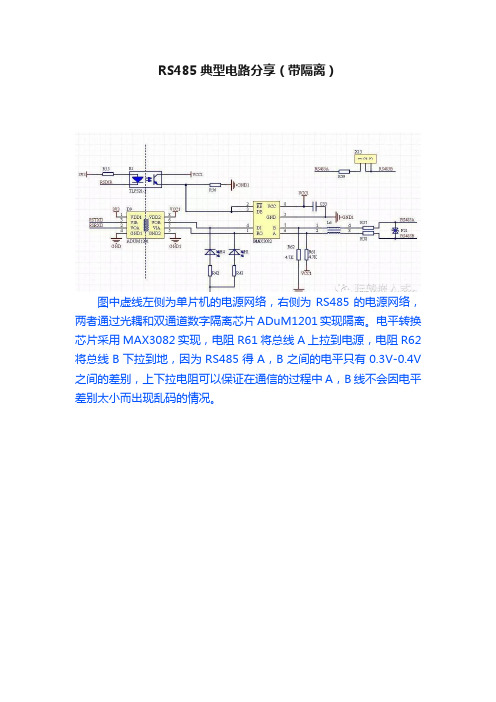
RS485典型电路分享(带隔离)
图中虚线左侧为单片机的电源网络,右侧为RS485的电源网络,两者通过光耦和双通道数字隔离芯片ADuM1201实现隔离。电平转换芯片采用MAX3082实现,电阻R61将总线A上之间的电平只有0.3V-0.4V之间的差别,上下拉电阻可以保证在通信的过程中A,B线不会因电平差别太小而出现乱码的情况。
ADI ADM2867E5和电源隔离RS-485解决方案

ADI ADM2867E5.7 kV RMS信号和电源隔离RS-485收发器解决方案ADI公司的ADM2867E是配备±15 kV IEC ESD 的5.7 kV RMS 信号和电源隔离式RS-485/RS-422 收发器.ESD保护在RS-475A,B,Y和Z引脚,接触放电≥±12 kV IEC61000-4-2,空气放≥±15kV IEC61000-4-2,高速25Mbps数据速率(ADM2865E/ADM2867E),低速数据速率500kbps用来EMI控制(ADM2861E/ADM2863E).输入VCC电源3V-5.5V,逻辑VIO电源1.7V-5.5V,VSEL引脚可选择VISO 电源5V或3.3V, PROFIBUS和5V VISO兼容,宽敞工作温度−40℃到+105℃,共模瞬态免疫力高,为250 kV/μs,支持196总线节点,器件具有短路保护,开路保护和浮动输入接收器自动防止故障性能.主要用在VC网络,工业现场总线,建筑物自动化,公用事业网络和能量表. 为您整理如下详细资料,本文介绍了ADM2867E主要特性,功能框图,电路连接图以及评估板EVAL-ADM2867EEBZ主要特性,电路图.The ADM2867E and the pending products within this family (light blue at the top of each page and gray in text) are 5.7 kV rms signal and power isolated RS-485 transceivers. The devices passradiated emissions testing to the EN55032 Class B standard with margin on a 2-layer printed circuit board (PCB) using two smallexternal 0402 ferrites on isolated power and ground pins. Thedevice features an integrated, low electromagnetic interference(EMI), isolated dc-to-dc converter, which eliminates the need for an external isolated power supply. The isolation barrierprovides immunity to system level electromagnetic compatibility (EMC) standards. The family of isolator devices features ±12 kV contact and ±15 kV airIEC61000-4-2 ESD protection on theRS-485 A, B, Y, and Z pins. The devices also features cable invert pins, allowing the user to quickly correct reversed cable connection on the A, B, Y, and Z bus pins while maintaining full receiver fail-safe performance. Slew rate limited versions are available, which are optimized for low speed over long cable runs, and have a maximum data rateof 500 kbps. Half duplex and full duplex variants are available. The full duplex generics allow independent cable inversion of the driver and receiver for additional flexibility.ADM2867E主要特性:5.7 kV rms isolated RS-485/RS-422 transceiverLow radiated emissions, integrated, isolated dc-to-dc converterPasses EN55032 Class B with margin on a 2-layer PCB Cable invert smart featureCorrect reversed cable connection on A, B, Y, and Z buspins while maintaining full receiver fail-safe featureESD protection on RS-485 A, B, Y, and Z pins≥±12 kV IEC61000-4-2 contact discharge≥±15 kV IEC61000-4-2 air dischargeHigh speed 25 Mbps data rate (ADM2865E/ADM2867E)Low speed 500 kbps data rate for EMI control(ADM2861E/ADM2863E)Flexible power suppliesInput VCC supply of 3 V to 5.5 VLogic VIO supply of 1.7 V to 5.5 VVSEL pin to select VISO supply of 5 V (VCC > 4.5 V) or 3.3 VPROFIBUS compliant for 5 V VISOWide operating temperature range: −40℃ to +105℃High common-mode transient immunity: 250 kV/μsShort-circuit, open-circuit, and floating input receiver fail-safeSupports 196 bus nodes (72 kΩ receiver input impedance)Full hot swap support (glitch free power-up/power-down)Safety and regulatory approvals (pending)CSA Component Acceptance Notice 5A, DIN V VDE V 0884-11,UL 1577, CQC11-471543-2012, IEC 61010-128-lead, fine pitch SOIC_W package (10.15 mm × 10.05 mm) with >8.0 mm creepage and clearance ADM2867E应用:Heating, ventilation, and air conditioning (HVAC) networksIndustrial field busesBuilding automationUtility networksEnergy meters图1.ADM2867E/ADM2863E功能框图图2.ADM2861E/ADM2865E功能框图图3.ADM2867E电路连接图评估板EVAL-ADM2867EEBZEvaluating the 5.7 kV RMS ADM2867E Signal and Power Isolated RS-485 Transceiver with ±15 kV IEC ESDThe EVAL-ADM2867EEBZ allows the simp lifi ed, efficient evaluation of the 5.7 kV rms ADM2867E signal and power isolated RS-485 transceiver. The ADM2867E features an integrated, isolated, dc-to-dc converter that provides power to the isolated side of the device with no additional ICs required. Anon-board ADP7104 low dropout (LDO) regulator accepts an input voltage of 3.3 V to 20 V and regulates the voltage to a selectable 3.3 V or 5 V supply for the VCC pin of the ADM2867E. The LDO regulator can be bypassed to power the VCC pin of the ADM2867E directly. A flexible logic VIO supply allows the device to operate with a digital input/output (I/O) voltage from 1.7 V to 5.5 V, which enable s communication with modern nodes using either a 1.8 V or 2.5 V power supply. The VIO pin can also be supplied from the ADP7104 regulated supply. The EVAL-ADM2867EEBZ comes with options to evaluate the ADM2867E inan individual system. Digital and RS-485 bus signals are accessible via the screw terminal blocks on the EVAL- ADM2867EEBZ. Each digital input can be configured via the on-board jumper options. Alternative methods can provide the transmit data input (TxD) signal to the device. An optional LTC6900 oscillator is included on the EVAL-ADM2867EEBZ and can be configured to provide a clock signal as the TxD digital input within a 1 kHz to 20 MHz range. For optimal signal integrity, use the on-board Su bm iniature Version A (SMA) connector to connect an external TxD signal at high data rates up to 25 Mbps. TheEVAL-ADM2867EEBZ has a footprint for the full duplex, isolated, RS-485 transceiver in a 10.15 mm ×10.05 mm, 28-lead, small outline, wide body with fine pitch (SOIC_W_FP) package. TheEVAL-ADM2867EEBZ is populated with the ADM2867E 5.7 kV rms, isolated RS-485 transceiver. For full details on the ADM2867E, see the ADM2867E data sheet, which must be used in conjunction with this user guide when using the EVAL-ADM2867EEBZ.评估板EVAL-ADM2867EEBZ主要特性:Simplified evaluation of the 25 Mbps ADM2867E RS-485 transceiver2-layer PCB compliant to EN 55032 Class B radiated emissionsFootprint for 10.15 mm × 10.05 mm, 28-lead SOIC_W_FP package with >8.0 mm creepage and clearance On-board ADP7104 LDO regulator with jumper options for simplified evaluation in 5 V or 3.3 V configuration Flexible, low voltage VIO supply rail to interface with I/O nodes as low as 1.7 V Selectable 3.3 V or 5 V isolated supply voltage options availableIEC 61000-4-2 ESD protection on the A, B, Y, and Z pins ±12 kV contact discharge and ±15 kV air discharge SMA connector for high speed 25 Mbps TxD input signalOptional on-board LTC6900 oscillator to provide TxD input signalScrew terminal blocks for power connections, digital signals, and RS-485 signalsJumper-selectable enable and disable for digital input signalsResistors and footprints for termination and loopback testTest points to measure all signals图4.评估板EVAL-ADM2867EEBZ外形图图5.评估板EVAL-ADM2867EEBZ电路图。
RS485隔离参考设计

Application ReportSLLA299–October2009Isolated RS-485Reference Design Thomas Kugelstadt ICP-Industrial InterfaceThis design note presents the reference designs of isolated RS-485nodes,using bus voltages of3.3V and5V.Various transceivers are used to satisfy the requirements for low,medium,and high data rates, as well as to accommodate the need for half-and full-duplex operation.Table1lists the family of isolated RS-485transceivers from Texas Instruments.Table1.Isolated RS-485TransceiversData Rate Rise Time[ns]Primary-Supply Secondary-Supply Device Transmission[Mbps](Typical)Voltage Range[V]Voltage Range[V] ISO30820.2900 3.15–5.5 4.5–5.5ISO15Half-duplex1185 3.15–3.6 3.15–3.6ISO3088207 3.15–5.5 4.5–5.5ISO30800.2900 3.15–5.5 4.5–5.5ISO35Full-duplex1185 3.15–3.6 3.15–3.6ISO3086207 3.15–5.5 4.5–5.5 Signal-Path IsolationAll transceivers present a1/8unit load to the bus,possess a4-kV peak isolation voltage,and have atypical transient immunity of50kV/µs.Whereas the ISO15and ISO35(shaded cells in Table1)operate from a3.3-V nominal supply on both the primary side and the secondary side,the transceivers of theISO308x family allow for mixed-supply operation.This is of particular advantage for applications operating in harsh industrial environments,because the3.3V on the primary side enables the connection tolow-voltage microcontrollers for power preservation,whereas the5V on the secondary side maintains a high signal-to-noise ratio when driving signals across long distances.Power Supply IsolationModern isolated power supplies are available as small,surface-mount modules.They often include the transformer driver,the actual isolation transformer,and the rectifier network.Sophisticated DC-DCmodules,such as the RSZ-3.33.3HP(3.3Vin/3.3Vout)and RSZ-3.305HP(3.3Vin/5Vout),even include a linear regulator with its associated bypass and output capacitors,while providing short-circuit protection and a solid,2-kV isolation voltage.Noise and Transient SuppressionFor effective transient protection,a low-capacitive transient voltage suppressor(TVS),such as PSM712,is recommended.The device provides a600-W surge capability,75pF of capacitance,and up to40-kV ESD protection,while its stand-off voltages cover the RS-485common-mode range of–7V to+12V.Implementation of additional noise filtering to the signal paths between the node controller and thesingle-ended side of the transceiver through simple R-C low-pass filters is recommended.Calculate thefilter component values such that RF ×CF=0.032/fSwith fSbeing the highest signal frequency of interest.System DiagramsFigure1shows the system diagram for a3.3-V/5-V,half-duplex network node using ISO3082for signal isolation and RSZ-3.305HP for power isolation.Figure2shows the system diagram for a3.3-V/3.3-V,full-duplex network node using ISO35for signal isolation and RSZ-3.33.3HP for power isolation.1 SLLA299–October2009Isolated RS-485Reference Design Submit Documentation FeedbackCopyright©2009,Texas Instruments IncorporatedReferences ReferencesFor more specific information on devices presented in this design note,see one of the following links:•For isolated RS-485transceivers see •For isolated DC-to-DC modules see or •For transient voltage suppressors see Figure1.2-kV,Isolated RS-485Node for200-kbps,Half-Duplex Operation2Isolated RS-485Reference Design SLLA299–October2009Submit Documentation FeedbackCopyright©2009,Texas Instruments Incorporated ReferencesFigure2.2-kV,Isolated RS-485node for1-Mbps,Full-Duplex Operation3 SLLA299–October2009Isolated RS-485Reference Design Submit Documentation FeedbackCopyright©2009,Texas Instruments IncorporatedIMPORTANT NOTICETexas Instruments Incorporated and its subsidiaries(TI)reserve the right to make corrections,modifications,enhancements,improvements, and other changes to its products and services at any time and to discontinue any product or service without notice.Customers should obtain the latest relevant information before placing orders and should verify that such information is current and complete.All products are sold subject to TI’s terms and conditions of sale supplied at the time of order acknowledgment.TI warrants performance of its hardware products to the specifications applicable at the time of sale in accordance with TI’s standard warranty.Testing and other quality control techniques are used to the extent TI deems necessary to support this warranty.Except where mandated by government requirements,testing of all parameters of each product is not necessarily performed.TI assumes no liability for applications assistance or customer product design.Customers are responsible for their products and applications using TI components.To minimize the risks associated with customer products and applications,customers should provide adequate design and operating safeguards.TI does not warrant or represent that any license,either express or implied,is granted under any TI patent right,copyright,mask work right, or other TI intellectual property right relating to any combination,machine,or process in which TI products or services are rmation published by TI regarding third-party products or services does not constitute a license from TI to use such products or services or a warranty or endorsement e of such information may require a license from a third party under the patents or other intellectual property of the third party,or a license from TI under the patents or other intellectual property of TI.Reproduction of TI information in TI data books or data sheets is permissible only if reproduction is without alteration and is accompanied by all associated warranties,conditions,limitations,and notices.Reproduction of this information with alteration is an unfair and deceptive business practice.TI is not responsible or liable for such altered rmation of third parties may be subject to additional restrictions.Resale of TI products or services with statements different from or beyond the parameters stated by TI for that product or service voids all express and any implied warranties for the associated TI product or service and is an unfair and deceptive business practice.TI is not responsible or liable for any such statements.TI products are not authorized for use in safety-critical applications(such as life support)where a failure of the TI product would reasonably be expected to cause severe personal injury or death,unless officers of the parties have executed an agreement specifically governing such use.Buyers represent that they have all necessary expertise in the safety and regulatory ramifications of their applications,and acknowledge and agree that they are solely responsible for all legal,regulatory and safety-related requirements concerning their products and any use of TI products in such safety-critical applications,notwithstanding any applications-related information or support that may be provided by TI.Further,Buyers must fully indemnify TI and its representatives against any damages arising out of the use of TI products in such safety-critical applications.TI products are neither designed nor intended for use in military/aerospace applications or environments unless the TI products are specifically designated by TI as military-grade or"enhanced plastic."Only products designated by TI as military-grade meet military specifications.Buyers acknowledge and agree that any such use of TI products which TI has not designated as military-grade is solely at the Buyer's risk,and that they are solely responsible for compliance with all legal and regulatory requirements in connection with such use. TI products are neither designed nor intended for use in automotive applications or environments unless the specific TI products are designated by TI as compliant with ISO/TS16949requirements.Buyers acknowledge and agree that,if they use any non-designated products in automotive applications,TI will not be responsible for any failure to meet such requirements.Following are URLs where you can obtain information on other Texas Instruments products and application solutions:Products ApplicationsAmplifiers Audio /audioData Converters Automotive /automotiveDLP®Products Broadband /broadbandDSP Digital Control /digitalcontrolClocks and Timers /clocks Medical /medicalInterface Military /militaryLogic Optical Networking /opticalnetworkPower Mgmt Security /securityMicrocontrollers Telephony /telephonyRFID Video&Imaging /videoRF/IF and ZigBee®Solutions /lprf Wireless /wirelessMailing Address:Texas Instruments,Post Office Box655303,Dallas,Texas75265Copyright©2009,Texas Instruments Incorporated。
485隔离芯片参考电路

485隔离芯片参考电路485隔离芯片参考电路是一种常用于工业自动化领域的电子设备,用于解决信号隔离和传输过程中的干扰问题。
本文将介绍485隔离芯片参考电路的原理、组成部分以及应用。
1.原理485隔离芯片参考电路基于RS-485通信标准,采用差分传输方式来抵抗干扰。
其主要原理是通过差分传输,将信号分为两路正负极性相反的信号进行传输。
在发送端,芯片接收到逻辑信号后将其转换成差分信号,并通过输出端口发送到接收端。
在接收端,芯片将接收到的差分信号转换为逻辑信号,以达到数据的传输和隔离。
2.组成部分485隔离芯片参考电路主要包括发送端、接收端和隔离部分。
其中,发送端包括发送器、驱动器和电路保护部分;接收端包括接收器、解码器和电路保护部分;隔离部分包括隔离变压器和隔离器。
2.1发送端发送信号经过发送器引脚输入到驱动器,驱动器将逻辑信号转换为差分信号,并通过电路保护部分对信号进行电气保护,防止过压和过流。
2.2接收端接收端接收到差分信号后,经过电路保护部分进行电气保护,然后通过接收器将差分信号转换为逻辑信号,再经过解码器将逻辑信号转换为数据信号。
2.3隔离部分隔离部分主要由隔离变压器和隔离器组成。
隔离变压器用于实现信号的电气隔离,阻断信号的传导路径,降低传导干扰。
隔离器用于传输隔离的数据信号,实现信号的逻辑隔离。
3.应用485隔离芯片参考电路广泛应用于工业自动化领域,例如工业控制系统、仪器仪表、电力监测、通信设备等。
其主要优势包括:3.1抗干扰能力强485隔离芯片参考电路采用差分传输方式,具有抗干扰能力强的特点。
差分传输将信号分为两路正负极性相反的信号进行传输,可以减少干扰对信号的影响。
3.2传输距离远485隔离芯片参考电路能够实现较长距离的信号传输。
485通信标准规定了最大传输距离为1200米,能够满足工业自动化领域对信号传输的要求。
3.3多设备共享总线485隔离芯片参考电路支持多设备共享总线,能够实现多个设备之间的数据传输和通信。
采用ADM2483的隔离RS-485中继器设计
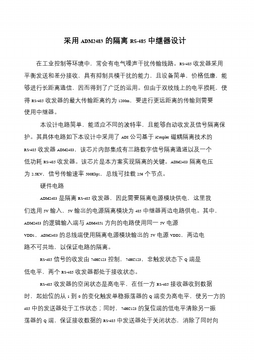
采用ADM2483的隔离RS-485中继器设计
在工业控制等环境中,常会有电气噪声干扰传输线路。
RS-485收发器采用平衡发送和差分接收,具有抑制共模干扰的能力,且设备简单,价格低廉,能够进行长距离通信,因而得到了广泛的运用。
但由于双绞线上的电平损耗,使得RS-485收发器的最大传输距离约为1200m,要进行更远距离的传输则需要使用中继器。
本设计电路简单,能适应不同的波特率,且能够自动收发及信号隔离保护。
其具体电路如下本设计中采用了ADI公司基于iCoupler磁耦隔离技术的RS-485收发器ADM2483,该芯片内部集成有三路数字信号隔离通道以及一个低功耗RS-485收发器。
该芯片是本方案实现隔离的关键。
ADM2483隔离电压为2.5KV,信号传输速率500Kbps,总线可挂载256个节点。
硬件电路
ADM2483是隔离RS-485收发器,因此需要隔离电源模块供电,这里我们选用5V输入,5V输出的电源隔离模块为485中继器两边电路供电。
其中,ADM2483的逻辑输入端与ADM4851方向的电路使用同一5V电源
VDD1,ADM2483的总线端使用隔离电源模块输出的5V电源VDD2,两边电路不可共地,以保证电路的隔离。
RS-485信号的收发由74HC123控制,74HC123,非触发状态下Q端是低电平,两个RS-485收发器都处于接收状态。
RS-485收发器的空闲状态是高电平,在任一方RS-485接收器收到数据时,起始位的从1到0的变化触发单稳振荡器的Q端变为高电平,使另一方的485中的发送器处于工作状态;同时,74HC123的复位端的低电平清除另一振荡器的Q端,保证接收数据的RS-485中发送器处于关闭状态,消除了同时向。
RS485端口隔离及保护设计
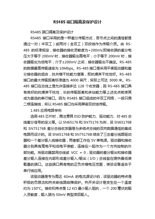
RS485端口隔离及保护设计RS485端口隔离及保护设计RS485接口采用的是一种差分传输方式,各节点之间的通信都是通过一对(半双工)或两对(全双工)双绞线作为传输介质。
由RS-485的标准规定,接收器的接收灵敏度为+200mV,即接收端的差分电压大于等于200mV时,接收器输出高电平;小于等于200mV时,接收器输出为低电平;介于±200mV之间,接收器输出不确定。
RS-485的数据最高传输速率为10Mbps。
RS-485接口是采用平衡驱动器和差分接收器的组合,抗共模干扰能力增强,即抗噪声干扰性好。
RS-485接口的最大传输距离标准值为4000英尺,实际上可达3000米。
RS-485接口在总线上是允许连接多达128个收发器,因RS-485接口具有良好的抗噪声干扰性,长的传输距离和多站能力等上述优点就使其成为首选的串行接口。
因为RS485接口组成的半双工网络,一般只需二根连接线,所以RS485接口均采用屏蔽双绞线传输。
1.485应用电路举例选用485芯片时,需注意其ESD防护能力、驱动能力、对485总线差分信号的定义等。
以SN65176和SN75176为例,该SN65176B 和SN75176B差分总线收发器是为多结点总线的双向数据通信的集成电路而设计的。
该SN65176B和SN75176B结合了三态差分线路驱动器和一个差分输入线接收器,两者都工作在5V单电源。
驱动器和接收器分别具有高电平和低电平使能,连接在一起作为一个方向控制的外部功能。
当驱动器禁用总线或VCC = 0,驱动器的差分输出和接收器差分输入连接在内部形成差分输入/输出(I/O)总线旨在提供最低装载量的端口。
这些端口具有宽的正负共模电压范围,使该设备适合于串行线应用。
该驱动器是专为高达60mA的电流源设计的,该驱动器的特点是积极的负限流和热关断线路故障保护。
热开关设计是发生在一个温度约为150°C。
接收机特点是12 KΩ最小输入阻抗,一个200毫伏的输入灵敏度,输入端为50mV典型滞后输入。
带隔离的485和CAN原理图

Application ReportSLLA299–October2009Isolated RS-485Reference Design Thomas Kugelstadt ICP-Industrial InterfaceThis design note presents the reference designs of isolated RS-485nodes,using bus voltages of3.3V and5V.Various transceivers are used to satisfy the requirements for low,medium,and high data rates, as well as to accommodate the need for half-and full-duplex operation.Table1lists the family of isolated RS-485transceivers from Texas Instruments.Table1.Isolated RS-485TransceiversData Rate Rise Time[ns]Primary-Supply Secondary-Supply Device Transmission[Mbps](Typical)Voltage Range[V]Voltage Range[V] ISO30820.2900 3.15–5.5 4.5–5.5ISO15Half-duplex1185 3.15–3.6 3.15–3.6ISO3088207 3.15–5.5 4.5–5.5ISO30800.2900 3.15–5.5 4.5–5.5ISO35Full-duplex1185 3.15–3.6 3.15–3.6ISO3086207 3.15–5.5 4.5–5.5 Signal-Path IsolationAll transceivers present a1/8unit load to the bus,possess a4-kV peak isolation voltage,and have atypical transient immunity of50kV/µs.Whereas the ISO15and ISO35(shaded cells in Table1)operate from a3.3-V nominal supply on both the primary side and the secondary side,the transceivers of theISO308x family allow for mixed-supply operation.This is of particular advantage for applications operating in harsh industrial environments,because the3.3V on the primary side enables the connection tolow-voltage microcontrollers for power preservation,whereas the5V on the secondary side maintains a high signal-to-noise ratio when driving signals across long distances.Power Supply IsolationModern isolated power supplies are available as small,surface-mount modules.They often include the transformer driver,the actual isolation transformer,and the rectifier network.Sophisticated DC-DCmodules,such as the RSZ-3.33.3HP(3.3Vin/3.3Vout)and RSZ-3.305HP(3.3Vin/5Vout),even include a linear regulator with its associated bypass and output capacitors,while providing short-circuit protection and a solid,2-kV isolation voltage.Noise and Transient SuppressionFor effective transient protection,a low-capacitive transient voltage suppressor(TVS),such as PSM712,is recommended.The device provides a600-W surge capability,75pF of capacitance,and up to40-kV ESD protection,while its stand-off voltages cover the RS-485common-mode range of–7V to+12V.Implementation of additional noise filtering to the signal paths between the node controller and thesingle-ended side of the transceiver through simple R-C low-pass filters is recommended.Calculate thefilter component values such that RF ×CF=0.032/fSwith fSbeing the highest signal frequency of interest.System DiagramsFigure1shows the system diagram for a3.3-V/5-V,half-duplex network node using ISO3082for signal isolation and RSZ-3.305HP for power isolation.Figure2shows the system diagram for a3.3-V/3.3-V,full-duplex network node using ISO35for signal isolation and RSZ-3.33.3HP for power isolation.1 SLLA299–October2009Isolated RS-485Reference Design Submit Documentation FeedbackCopyright©2009,Texas Instruments IncorporatedReferences ReferencesFor more specific information on devices presented in this design note,see one of the following links:•For isolated RS-485transceivers see •For isolated DC-to-DC modules see or •For transient voltage suppressors see Figure1.2-kV,Isolated RS-485Node for200-kbps,Half-Duplex Operation2Isolated RS-485Reference Design SLLA299–October2009Submit Documentation FeedbackCopyright©2009,Texas Instruments Incorporated ReferencesFigure2.2-kV,Isolated RS-485node for1-Mbps,Full-Duplex Operation3 SLLA299–October2009Isolated RS-485Reference Design Submit Documentation FeedbackCopyright©2009,Texas Instruments IncorporatedIMPORTANT NOTICETexas Instruments Incorporated and its subsidiaries(TI)reserve the right to make corrections,modifications,enhancements,improvements, and other changes to its products and services at any time and to discontinue any product or service without notice.Customers should obtain the latest relevant information before placing orders and should verify that such information is current and complete.All products are sold subject to TI’s terms and conditions of sale supplied at the time of order acknowledgment.TI warrants performance of its hardware products to the specifications applicable at the time of sale in accordance with TI’s standard warranty.Testing and other quality control techniques are used to the extent TI deems necessary to support this warranty.Except where mandated by government requirements,testing of all parameters of each product is not necessarily performed.TI assumes no liability for applications assistance or customer product design.Customers are responsible for their products and applications using TI components.To minimize the risks associated with customer products and applications,customers should provide adequate design and operating safeguards.TI does not warrant or represent that any license,either express or implied,is granted under any TI patent right,copyright,mask work right, or other TI intellectual property right relating to any combination,machine,or process in which TI products or services are rmation published by TI regarding third-party products or services does not constitute a license from TI to use such products or services or a warranty or endorsement e of such information may require a license from a third party under the patents or other intellectual property of the third party,or a license from TI under the patents or other intellectual property of TI.Reproduction of TI information in TI data books or data sheets is permissible only if reproduction is without alteration and is accompanied by all associated warranties,conditions,limitations,and notices.Reproduction of this information with alteration is an unfair and deceptive business practice.TI is not responsible or liable for such altered rmation of third parties may be subject to additional restrictions.Resale of TI products or services with statements different from or beyond the parameters stated by TI for that product or service voids all express and any implied warranties for the associated TI product or service and is an unfair and deceptive business practice.TI is not responsible or liable for any such statements.TI products are not authorized for use in safety-critical applications(such as life support)where a failure of the TI product would reasonably be expected to cause severe personal injury or death,unless officers of the parties have executed an agreement specifically governing such use.Buyers represent that they have all necessary expertise in the safety and regulatory ramifications of their applications,and acknowledge and agree that they are solely responsible for all legal,regulatory and safety-related requirements concerning their products and any use of TI products in such safety-critical applications,notwithstanding any applications-related information or support that may be provided by TI.Further,Buyers must fully indemnify TI and its representatives against any damages arising out of the use of TI products in such safety-critical applications.TI products are neither designed nor intended for use in military/aerospace applications or environments unless the TI products are specifically designated by TI as military-grade or"enhanced plastic."Only products designated by TI as military-grade meet military specifications.Buyers acknowledge and agree that any such use of TI products which TI has not designated as military-grade is solely at the Buyer's risk,and that they are solely responsible for compliance with all legal and regulatory requirements in connection with such use. TI products are neither designed nor intended for use in automotive applications or environments unless the specific TI products are designated by TI as compliant with ISO/TS16949requirements.Buyers acknowledge and agree that,if they use any non-designated products in automotive applications,TI will not be responsible for any failure to meet such requirements.Following are URLs where you can obtain information on other Texas Instruments products and application solutions:Products ApplicationsAmplifiers AudioData Converters AutomotiveDLP®Products BroadbandDSP Digital ControlClocks and Timers MedicalInterface MilitaryLogic Optical NetworkingPower Mgmt SecurityMicrocontrollers TelephonyRFID Video&ImagingRF/IF and ZigBee®Solutions WirelessMailing Address:Texas Instruments,Post Office Box655303,Dallas,Texas75265Copyright©2009,Texas Instruments Incorporated。
485隔离芯片参考电路
485隔离芯片参考电路485隔离芯片参考电路是一种常用的隔离芯片,具有高性能、低功耗和多功能等特点。
本文将介绍485隔离芯片参考电路的工作原理、性能优势和应用领域。
一、工作原理485隔离芯片参考电路是由Silicon Labs公司制造的隔离芯片,具有高速数据传输、低功耗和多功能的优点。
该芯片的工作原理是基于Silicon Labs公司独有的Active-Cloze技术,能够实现数据在传输过程中的高速传输和低功耗。
二、性能优势485隔离芯片参考电路具有以下高性能优势:1.高速数据传输485隔离芯片参考电路能够实现100Mbps的数据传输速度,满足高速数据传输的需求。
该芯片还支持自适应信号传输,能够根据网络环境的变化自动调整传输速度,保证数据传输的稳定性和可靠性。
2.低功耗485隔离芯片参考电路具有低功耗的特点,能够在满足高性能要求的同时实现长时间的电池寿命。
该芯片的功耗仅为5V,非常适合用于需要长时间工作的应用场景。
3.多功能485隔离芯片参考电路具有多功能的特点,支持多种协议,包括RS485、CAN、SPI等。
该芯片还具有独特的安全特性,能够防止数据在传输过程中被窃听或篡改,保证数据的安全性。
三、应用领域485隔离芯片参考电路可以应用于多种领域,包括数据传输、工业自动化、电动汽车等。
该芯片可以连接到各种设备,如PLC、RFID、工业自动化机器人等,实现设备之间的数据传输和远程控制。
四、结论485隔离芯片参考电路是一种高性能、低功耗和多功能的芯片,具有广泛的应用领域。
该芯片可以应用于各种需要高速数据传输、低功耗和安全性能需求的场景中,为各种物联网应用、工业自动化和智能家居等提供了重要的支持。
- 1、下载文档前请自行甄别文档内容的完整性,平台不提供额外的编辑、内容补充、找答案等附加服务。
- 2、"仅部分预览"的文档,不可在线预览部分如存在完整性等问题,可反馈申请退款(可完整预览的文档不适用该条件!)。
- 3、如文档侵犯您的权益,请联系客服反馈,我们会尽快为您处理(人工客服工作时间:9:00-18:30)。
一种自带隔离电源的RS-485隔离芯片电路参考设计
RS-485标准是一种常见的总线架构,其通用性及远距离传输能力使其广泛应用于各种通信接口电路。
在多数情况下,由于应用环境的恶劣,需要对RS-485接口采用隔离方案以防止出现接地环路。
对RS-485接口的隔离方案有很多,老式的光耦隔离电路由于占用空间、体积太大,需要分立元件、缓存驱动及电路设计繁琐,已经不适合应用于当今要求越来越严格的高速数字通信系统。
因此,我们可以采用ADI公司的iCoupler磁隔离解决方案,它能够提供多通道数字隔离、集成RS-485收发器的数字隔离、集成isoPower磁隔离电源的数字隔离等多种灵活的隔离方案。
在体积、功耗、速率等众多方面提供优于光耦的解决方案。
在这里,我们了解一下目前最简单,集成度最高的RS-485接口隔离方案。
本方案采用隔离型RS-485收发器ADM2582E/ADM2587E,以单芯片实现完全的半/全双工RS-485接口隔离。
ADM2582E/ADM2587E集成isoPower磁隔离电源,无需外部隔离电源供电。
在单芯片封装内还集成了数字隔离通道和RS-485收发器,与传统光耦隔离电路相比,PCB面积缩小84%,元器件数减少83%。
ADM2582E/ADM2587E是具备±15 kV ESD保护功能的完全集成式隔离数据收发器,适合用于多点传输线路上的高速通信应用。
其内部集成的RS-485驱动器带有一个高电平有效使能电路,并且还提供一个高电平接收机有效禁用电路,可使接收机输出进入高阻抗状态。
该器件具备限流和过热关断特性,能够防止输出短路,并防止出现由于总线争用而引起功耗过大的情况。
图1、ADM2582E/ADM2587E功能框图
根据ADM2582E/ADM2587E的功能框图,我们可以看出其内部含有isoPower技术,具有反馈控制的高频开关稳压电路。
对于TxD、RxD、DE和RE均采用iCoupler磁隔离技术对其数字信号进行隔离。
此外,还包含一个能够实现半/全双工的RS-485/RS- 422收发器。
以单芯片实现了能适应各种需求的RS-485/RS-422接口隔离方案,其芯片封装仅为SOIC-20。
ADM2582E/ADM2587E通过简单的外部电路连接即可实现接口隔离功能,下面以ADM2587E为例,来实现半双工和全双工的RS-485/RS-422接口隔离。
半双工隔离ADM2587E带有RE/DE使能控制引脚,能够支持半双工应用,其应用电路图如下:
图2、ADM2587E用于半双工RS-485/RS-422接口隔离
由于ADM2587E后端有A、B、Y、Z四路输出,当用作半双工电路时,需要将A和Y连接,作为半双工的A信号线,将B和Z连接,作为半双工的B信号线。
两个VCC引脚的输入端和GND1引脚之间接有0.01uF、10uF及2个0.1uF电容,这些电容是必要的,能够去耦及滤波,保证输入电源的平稳。
同样,Visoin与GND2引脚之间的0.1uF和0.01uF电容,Visoout和GND2引脚之间的0.1uF和10uF电容都是芯片工作所需要的。
在ADM2587E的总线输出侧的Visoin引脚和Visoout引脚必须连接在一起,从图1的功能框图中我们可以看到,Visoout引脚是ADM2587E 内部隔离电源的输出引脚,而Visoin引脚是内部集成RS-485/RS-422收发器的电源输入引脚。
全双工隔离ADM2587E的全双工隔离电路非常简单,将逻辑侧引脚与控制芯片连接,总线侧引脚与总线相接即可。
其应用电路图如下:
图3、ADM2587E用于全双工RS-485/RS-422接口隔离
ADM2587E的全双工隔离电路与半双工隔离电路类似,其后端的A、B、Y、Z直接与全双工总线相连即可。
结语
ADM2582E/ADM2587E均可采用3.3V或5V供电,能够方便的与普通5V供电系统和低功耗的3.3V供电系统连接。
A、B、Y、Z引脚上带有±15KV的ESD保护及25KV/us的共模抑制能力,能够为芯片引脚提供大部分的保护功能,在恶劣的应用环境中,可以在总线上添加TVS管等器件以增强芯片对大的浪涌电流、电压的防护能力。
总的来说,ADM2582E/ADM2587E集成度高,外围电路简单,整体性能稳定,非常适合于工业、电力等恶劣通信环境中的RS- 485/RS-422接口隔离应用。