SVD1N60DB说明书_1.2-L
USN60使用说明书4B

4.5导向进入数据库文件和附加注释厚度测量可以存储在数据库文件中(参见5.1创建数据库文件)。
数据库文件被创建后,操作者可以选择指定的文件位置并启动,然后按键在此位置存储厚度读数(参见5.2存储厚度读数)。
操作者也可以附加一个或多个注释到每个数据库文件位置。
通过数据库文件内容导向:第一步:确保选择文件名功能(位于文件子菜单中)后,数据库文件打开。
(视图不适用于数据建立文件,因为它们不包括厚度测量)第二步:启动测试菜单。
第三步:按VIEW(视图)选项下面的键。
第四步:按照导向指导如图4-5所示附加注释。
注意:通过设置NOTE ACTION功能为DISPLAY NOTES,可显示所有注释。
第五步:如果你想返回到测试菜单栏,按下键,你可以通过按下NOTES选项下面的键重新进入注释选择栏。
图4-5显示选项允许操作者在导向进入数据库文件时查看A-扫描可以看到此视图内容和当前数据库文件的附加注释。
1:下半部分只显示数据库文件内容2:所选数据库文件的位置名3:存储的厚度值(当COPY MODE设置为LOG TO FILE时,按下键存储所选文件位置的大显示框内容。
)4:按键显示测试菜单选项。
按NOTE(注释)选项下的键返回注释选择栏。
5:选择要启动的文件6:启动SCROLL FILE允许操作者用此键或功能旋钮导向进入文件位置。
7:通过单独注释键指定启动(增加或删除选择文件位置注释或全部注释)。
8:清除所选位置的值和附加注释。
9:按下后加上或删除NOTE(注释)D至或从所选文件位置(参见上面的NOTE ACTIVE键)(参见第5.7节编辑注释)4.6放大一个门的内容无论何时A扫描处于使用中并且测试菜单被启动,按下放大特征下面的键放大包含在指定门中的A 扫描显示部分。
任何可获得的门都可以被指定。
被放大门的宽度决定了放大的水平。
这是因为显示要在门宽等于100%全屏时才能被放大。
(如图4-6)显示将包含放大的视图直到按下键再一次选择放大。
FTD1N60规格书

General Features
Low ON Resistance Low Gate Charge (typical 4.8nC) Fast Switching 100% Avalanche Tested RoHS Compliant Halogen-free available
ISM
Maximum Pulsed Current(Body Diode)
VSD Diode Forward Voltage
trr
Reverse Recovery Time
Qrr
Reverse Recovery Charge
FTU01N60/FTD01N60
TC=25℃ unless otherwise specified
--
0.6
-- V/℃
Reference to 25℃, ID=250µA
--
-- 20
VDS=600V, VGS=0V
IDSS
Drain-to-Source Leakage Current --
µA -- 100
VDS=480V, VGS=0V, TC=125℃
--
-- 100
IGSS
Gate-to-Source Leakage Current
NOTE:
[1] TJ=+25℃ to +150℃ [2] Repetitive rating, pulse width limited by maximum junction temperature. [3] ISD=1.0A, di/dt≤100A/µs, VDD≤BVDSS, TJ=+150℃ [4] Pulse width≤380µs; duty cycle≤2%.
100V NPN 达林顿接驱电源芯片 SOT23 产品说明书
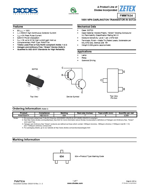
100V NPN DARLINGTON TRANSISTOR IN SOT23Features∙ BV CEO > 100V ∙ I C = 900mA high Continuous Collector Current ∙ I CM = 5A Peak Pulse Current ∙ 625mW Power dissipation ∙ h FE > 5k up to 2A for high current gain hold up ∙ Complementary PNP Type: FMMT734 ∙ Totally Lead-Free & Fully RoHS compliant (Notes 1 & 2) ∙ Halogen and Antimony Free. “Green” Device (Note 3) ∙ Qualified to AEC-Q101 Standards for High ReliabilityMechanical Data∙ Case: SOT23 ∙ Case Material: Molded Plastic, “Green” Molding CompoundUL Flammability Classification Rating 94V-0 ∙ Moisture Sensitivity: Level 1 per J-STD-020 ∙ Terminals: Finish – Matte Tin Plated Leads, Solderable perMIL-STD-202, Method 208 ∙ Weight 0.008 grams (approximate)Applications∙ Lamp ∙ Relay ∙ Solenoid DrivingOrdering Information (Note 4)Product Compliance Marking Reel size (inches) Tape width (mm)Quantity per reelFMMT634TA AEC-Q101 634 783,000Notes: 1. No purposely added lead. Fully EU Directive 2002/95/EC (RoHS) & 2011/65/EU (RoHS 2) compliant. 2. See /quality/lead_free.html for more information about Diodes Incorporated’s definitions of Halogen and Antimony free, "Green" and Lead-Free. 3. Halogen and Antimony free "Green” products are defined as those which contain <900ppm bromine, <900ppm chlorine (<1500ppm total Br + Cl) and <1000ppm antimony compounds.4. For packaging details, go to our website at /products/packages.htmlMarking Information634 = Product Type Marking CodeSOT23Top View Pin-OutTop ViewDevice SymbolCEB624634 EAbsolute Maximum Ratings(@T A = +25°C, unless otherwise specified.)UnitValueCharacteristic SymbolCollector-Base Voltage V CBO120 VCollector-Emitter Voltage V CEO100 VEmitter-Base Voltage V EBO12 VContinuous Collector Current I C900 mAPeak Pulse Current I CM 5 AThermal Characteristics (@T A = +25°C, unless otherwise specified.)UnitValueCharacteristic SymbolPower Dissipation (Note 5) P D625 mWPower Dissipation (Note 6) P D806 mWThermal Resistance, Junction to Ambient (Note 5) RθJA200 ︒C/WThermal Resistance, Junction to Ambient (Note 6) RθJA155 ︒C/WThermal Resistance, Junction to Leads (Note 7) RθJL194 ︒C/WOperating and Storage Temperature Range T J, T STG-55 to +150 ︒CESD Ratings (Note 8)UnitClassJEDECValueCharacteristic SymbolElectrostatic Discharge - Human Body Model ESD HBM 2,000 V 2Electrostatic Discharge - Machine Model ESD MM 200 V BNotes: 5. For a device mounted with the exposed collector pad on 25mm x 25mm 1oz copper that is on a single-sided 1.6mm FR4 PCB; device is measuredunder still air conditions whilst operating in a steady-state.6. Same as note (5), except the device is measured at t ≤ 5 sec.7. Thermal resistance from junction to solder-point (at the end of the collector lead).8. Refer to JEDEC specification JESD22-A114 and JESD22-A115.Thermal Characteristics and Derating information100m1101001m 10m100m110Single Pulse T amb =25°CV CE(s at)Limited100µs1ms10ms100ms1s DCSafe Operating AreaI C C o l l e c t o r C u r r e n t (A )V CE Collector-Emitter Voltage (V)2550751001251501750.00.10.20.30.40.50.60.7Derating CurveTemperature (°C)M a x P o w e r D i s s i p a t i o n (W )20406080100120140160180200220Transient Thermal ImpedanceT h e r m a l R e s i s t a n c e (°C /W )Pulse Width (s)0.1110100Pulse Power DissipationPulse Width (s)M a x i m u m P o w e r (W )Electrical Characteristics (@T A = +25°C, unless otherwise specified.)Characteristic Symbol Min Typ Max Unit Test ConditionCollector-Base Breakdown Voltage BV CBO 120 170 - V I C = 100µACollector-Emitter Breakdown Voltage (Note 9) BV CEO 100 115 - V I C = 10mAEmitter-Base Breakdown Voltage BV EBO 12 16 - V I E = 100µA Collector Cut-off Current I CBO - <1 10 nA V CB = 80V Emitter Cut-off Current I EBO - <1 10 nA V EB = 7V Collector Emitter Cut-off Current I CES - <1 100 nA V CES = 80VStatic Forward Current Transfer Ratio (Note 9) h FE- 20k 15k 5k - - 50k 60k 40k 14k 24k 600 ---- - - - I C = 10mA, V CE = 5V I C = 100mA, V CE = 5V I C = 1A, V CE = 5V I C = 2A, V CE = 5V I C = 1A, V CE = 2V I C = 5A, V CE = 5VCollector-Emitter Saturation Voltage (Note 9) V CE(sat)- - - - - - 0.67 0.72 0.75 0.82 0.68 0.85 0.750.800.850.93 - 0.96 V I C = 100mA, I B = 1mA I C = 250mA, I B = 1mA I C = 500mA, I B = 5mA I C = 900mA, I B = 5mA I C = 900mA, I B = 5mA, T J =+150°C I C = 1A, I B = 5mABase-Emitter Saturation Voltage (Note 9) V BE(sat) - 1.5 1.65 V I C = 1A, I B = 5mA Base-Emitter Turn-On Voltage (Note 9) V BE(on) - 1.33 1.50 V I C = 1A, V CE = 5VTransition Frequency f T- 140 - MHz I C = 50mA, V CE = 10V,f = 100MHzOutput Capacitance C obo - 9 20 pF V CB = 10V, f = 1MHz Turn-On Time t (on) - 290 - ns V CC = 20V, I C = 500mA,I B1 = -I B2 = 1mATurn-Off Time t (off) - 2,400 - ns Notes:9. Measured under pulsed conditions. Pulse width ≤ 300µs. Duty cycle ≤ 2%Typical Electrical Characteristics (@T A = +25°C, unless otherwise specified.)Package Outline DimensionsPlease see AP02002 at /datasheets/ap02002.pdf for latest version.Suggested Pad LayoutPlease see AP02001 at /datasheets/ap02001.pdf for the latest version.Note:For high voltage applications, the appropriate industry sector guidelines should be considered with regards to creepage and clearance distancesbetween device Terminals and PCB tracking.SOT23Dim Min Max Typ A 0.37 0.51 0.40 B 1.20 1.40 1.30 C 2.30 2.50 2.40 D 0.89 1.03 0.915 F 0.45 0.60 0.535 G 1.78 2.05 1.83 H 2.80 3.00 2.90 J 0.013 0.10 0.05 K 0.890 1.00 0.975 K1 0.903 1.10 1.025 L 0.45 0.61 0.55 L1 0.25 0.55 0.40 M 0.085 0.150 0.110 a 8°All Dimensions in mmDimensions Value (in mm)Z 2.9 X 0.8 Y 0.9C2.0 E1.35 X EYCZA l l 7°IMPORTANT NOTICEDIODES INCORPORATED MAKES NO WARRANTY OF ANY KIND, EXPRESS OR IMPLIED, WITH REGARDS TO THIS DOCUMENT, INCLUDING, BUT NOT LIMITED TO, THE IMPLIED WARRANTIES OF MERCHANTABILITY AND FITNESS FOR A PARTICULAR PURPOSE (AND THEIR EQUIVALENTS UNDER THE LAWS OF ANY JURISDICTION).Diodes Incorporated and its subsidiaries reserve the right to make modifications, enhancements, improvements, corrections or other changes without further notice to this document and any product described herein. Diodes Incorporated does not assume any liability arising out of the application or use of this document or any product described herein; neither does Diodes Incorporated convey any license under its patent or trademark rights, nor the rights of others. Any Customer or user of this document or products described herein in such applications shall assume all risks of such use and will agree to hold Diodes Incorporated and all the companies whose products are represented on Diodes Incorporated website, harmless against all damages.Diodes Incorporated does not warrant or accept any liability whatsoever in respect of any products purchased through unauthorized sales channel. Should Customers purchase or use Diodes Incorporated products for any unintended or unauthorized application, Customers shall indemnify and hold Diodes Incorporated and its representatives harmless against all claims, damages, expenses, and attorney fees arising out of, directly or indirectly, any claim of personal injury or death associated with such unintended or unauthorized application.Products described herein may be covered by one or more United States, international or foreign patents pending. Product names and markings noted herein may also be covered by one or more United States, international or foreign trademarks.This document is written in English but may be translated into multiple languages for reference. Only the English version of this document is the final and determinative format released by Diodes Incorporated.LIFE SUPPORTDiodes Incorporated products are specifically not authorized for use as critical components in life support devices or systems without the express written approval of the Chief Executive Officer of Diodes Incorporated. As used herein:A. Life support devices or systems are devices or systems which:1. are intended to implant into the body, or2. support or sustain life and whose failure to perform when properly used in accordance with instructions for use provided in thelabeling can be reasonably expected to result in significant injury to the user.B. A critical component is any component in a life support device or system whose failure to perform can be reasonably expected to cause thefailure of the life support device or to affect its safety or effectiveness.Customers represent that they have all necessary expertise in the safety and regulatory ramifications of their life support devices or systems, and acknowledge and agree that they are solely responsible for all legal, regulatory and safety-related requirements concerning their products and any use of Diodes Incorporated products in such safety-critical, life support devices or systems, notwithstanding any devices- or systems-related information or support that may be provided by Diodes Incorporated. Further, Customers must fully indemnify Diodes Incorporated and its representatives against any damages arising out of the use of Diodes Incorporated products in such safety-critical, life support devices or systems.Copyright © 2014, Diodes Incorporated。
优利德 UTS1000B系列使用手册 说明书

UTS1000B/T系列频谱分析仪用户手册REV12023.10尊敬的用户:您好!感谢您选购全新的优利德仪器,为了正确使用本仪器,请您在本仪器使用之前仔细阅读本使用手册全文,特别有关“安全注意事项”的部分。
如果您已经阅读完本使用手册全文,建议您将此使用手册进行妥善的保管,与仪器一同放置或者放在您随时可以查阅的地方,以便在将来的使用过程中进行查阅。
UNI-T优利德科技(中国)股份有限公司版权所有。
UNI-T产品受中国或其他国家专利权的保护,包括已取得或正在申请的专利。
本公司保留更改产品规格和价格的权利。
UNI-T保留所有权利。
许可软件产品由UNI-T及其子公司或提供商所有,受国家版权法及国际条约规定的保护。
本文中的信息将取代所有以前出版的资料中的信息。
UNI-T是优利德科技(中国)股份有限公司[UNI-TREND TECHNOLOGY(CHINA)CO.,LTD]的注册商标。
如果原购买者自购买该产品之日起一年内,将该产品出售或转让给第三方,则保修期应为自原购买者从UNI-T或授权的UNI-T分销商购买该产品之日起一年内,附件和保险丝等不受此保证的保护。
如果在适用的保修期内证明产品有缺陷,UNI-T可自行决定是修复有缺陷的产品且不收部件和人工费用,或用同等产品(由UNI-T决定)更换有缺陷的产品,UNI-T作保修用途的部件、模块和更换产品可能是全新的,或者经修理具有相当于新产品的性能,所有更换的部件、模块和产品将成为UNI-T的财产。
以下提到的“客户”是指据声明本保证所规定权利的个人或实体。
为获得本保证承诺的服务,“客户”必须在适用的保修期内向UNI-T通报缺陷,并为服务的履行做适当安排,客户应负责将有缺陷的产品装箱并运送到UNI-T指定的维修中心,同时预付运费并提供原购买者的购买证明副本,如果产品要运送到UNI-T维修中心所在国范围内的地点,UNI-T应支付向客户送返产品的费用,如果产品送返到任何其他地点,客户应负责支付所有的运费、关税、税金及任何其他费用。
N沟道增强型高压功率MOS场效应晶体管SVD4N60D(F)(FG)(T)说明书_1.4-L
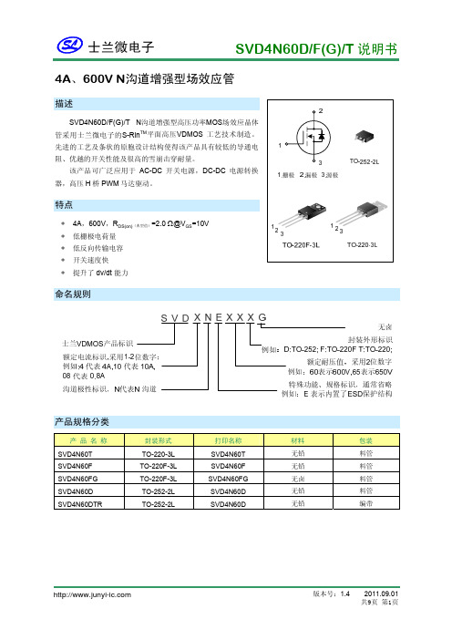
SVD4N60D/F(G)/T 说明书4A、600V N沟道增强型场效应管描述SVD4N60D/F(G)/T N沟道增强型高压功率MOS场效应晶体 管采用士兰微电子的S-RinTM平面高压VDMOS 工艺技术制造。
先进的工艺及条状的原胞设计结构使得该产品具有较低的导通电 阻、优越的开关性能及很高的雪崩击穿耐量。
该产品可广泛应用于 AC-DC 开关电源,DC-DC 电源转换 器,高压 H 桥 PWM 马达驱动。
特点∗ ∗ ∗ ∗ ∗4A,600V,RDS(on)(典型值)=2.0 Ω@VGS=10V 低栅极电荷量 低反向传输电容 开关速度快 提升了 dv/dt 能力命名规则产品规格分类产 品 名 称 SVD4N60T SVD4N60F SVD4N60FG SVD4N60D SVD4N60DTR 封装形式 TO-220-3L TO-220F-3L TO-220F-3L TO-252-2L TO-252-2L 打印名称 SVD4N60T SVD4N60F SVD4N60FG SVD4N60D SVD4N60D 材料 无铅 无铅 无卤 无铅 无铅 包装 料管 料管 料管 料管 编带版本号:1.42011.09.01 共9页 第1页SVD4N60D/F(G)/T 说明书极限参数(除非特殊说明,TC=25°C)参数名称 漏源电压 栅源电压 漏极电流 漏极脉冲电流 耗散功率(TC=25°C) - 大于 25°C 每摄氏度减少 单脉冲雪崩能量(注 1) 工作结温范围 贮存温度范围 TC=25°C TC=100°C 符号 VDS VGS ID IDM PD EAS TJ Tstg 100 0.8 参数范围 SVD4N60T SVD4N60F(G) 600 ±30 4.0 2.5 16 33 0.26 276 -55~+150 -55~+150 77 0.62 SVD4N60D 单位 V V A A W W/°C mJ °C °C热阻特性参数名称 芯片对管壳热阻 芯片对环境的热阻 符号 RθJC RθJA 参数范围 SVD4N60T 1.25 62.5 SVD4N60F(G) 3.85 120 SVD4N60D 1.61 110 单位 °C/W °C/W关键特性参数(除非特殊说明,TC=25°C)参 数 漏源击穿电压 漏源漏电流 栅源漏电流 栅极开启电压 导通电阻 输入电容 输出电容 反向传输电容 开启延迟时间 开启上升时间 关断延迟时间 关断下降时间 栅极电荷量 栅极-源极电荷量 栅极-漏极电荷量 符号 BVDSSB测试条件 VGS=0V,ID=250µA VDS=600V,VGS=0V VGS=±30V,VDS=0V VGS= VDS,ID=250µA VGS=10V, ID=2A VDS=25V,VGS=0V, f=1.0MHZ VDD=300V,ID=4A, RG=25Ω (注 2,3) VDS=480V,ID=4A, VGS=10V (注 2,3)最小值 600 --2.0 ------------典型值 ----2.0 672 66 4.7 27 19 160 22 19.8 4 7.2最大值 -10 ±100 4.0 2.4 -----------单位 V µA nA V ΩIDSS IGSS VGS(th) RDS(on) Ciss Coss Crss td(on) tr td(off) tf Qg Qgs QgdpFnsnC版本号:1.42011.09.01 共9页 第2页SVD4N60D/F(G)/T 说明书源-漏二极管特性参数参 源极电流 源极脉冲电流 源-漏二极管压降 反向恢复时间 反向恢复电荷 注: 1. 2. 3. L=30mH,IAS=3.81A,VDD=175V,RG=25Ω,开始温度 TJ=25°C; 脉冲测试: 脉冲宽度≤300μs,占空比≤2%; 基本上不受工作温度的影响。
1N60L规格书

UNISONIC TECHNOLOGIES CO., LTD1N60Power MOSFET1.2A,600V N-CHANNELPOWER MOSFET⏹DESCRIPTIONThe UTC 1N60 is a high voltage MOSFET and is designed tohave better characteristics, such as fast switching time, low gatecharge, low on-state resistance and have a high ruggedavalanche characteristics. This power MOSFET is usually used athigh speed switching applications in power supplies, PWM motorcontrols, high efficient DC to DC converters and bridge circuits.⏹FEATURES* R DS(ON) <11.5Ω@ V GS=10V, I D=0.6A* Ultra Low gate charge (typical 5.0nC)* Low reverse transfer capacitance (C RSS = typical 3.0 pF)* Fast switching capability* Avalanche energy specified* Improved dv/dt capability, high ruggedness⏹SYMBOL⏹ ORDERING INFORMATIONOrdering Number Package Pin AssignmentPackingLead Free Halogen Free 1 2 3- 1N60G-AA3-R SOT-223 G D S Tape Reel 1N60L-TA3-T 1N60G-TA3-T TO-220 G D S Tube 1N60L-TF2-T 1N60G-TF2-T TO-220F2 G D S Tube 1N60L-TF3-T 1N60G-TF3-T TO-220F G D S Tube 1N60L-TM3-T 1N60G-TM3-T TO-251 G D S Tube 1N60L-TMS-T 1N60G-TMS-T TO-251S G D S Tube 1N60L-TMS2-T 1N60G-TMS2-T TO-251S2 G D S Tube 1N60L-TMS4-T 1N60G-TMS4-T TO-251S4 G D STube 1N60L-TN3-R 1N60G-TN3-R TO-252 G D S Tape Reel 1N60L-TND-R 1N60G-TND-R TO-252D G D S Tape Reel 1N60L-T60-K 1N60G-T60-K TO-126 G D S Bulk 1N60L-T92-B 1N60G-T92-B TO-92 G D S Tape Box 1N60L-T92-K 1N60G-T92-K TO-92G D S Bulk⏹MARKINGPACKAGE MARKING■ ABSOLUTE MAXIMUM RATINGS (T C = 25°С, unless otherwise specified)PARAMETER SYMBOLRATINGS UNIT Drain-Source Voltage V DSS 600 V Gate-Source Voltage V GSS ±30 V Avalanche Current (Note 2) I AR 1.2 A Continuous Drain Current I D 1.2 A Pulsed Drain Current (Note 2) I DM 4.8 AAvalanche Energy Single Pulsed (Note 3)E AS 50 mJ Repetitive (Note 2) E AR 4.0 mJPeak Diode Recovery dv/dt (Note 4) dv/dt 4.5 V/nsPower Dissipation SOT-223P D8WTO-251/TO-252TO-252D/TO-251STO-251S2/ TO-251S428TO-220 40 TO-220F 21 TO-220F2 23 TO-92(T A=25°С) 1TO-126 12.5Junction Temperature T J +150 °СOperating Temperature T OPR-55 ~ +150 °СStorage Temperature T STG-55 ~ +150 °СNotes: 1. Absolute maximum ratings are those values beyond which the device could be permanently damaged.Absolute maximum ratings are stress ratings only and functional device operation is not implied.2. Repetitive Rating: Pulse width limited by maximum junction temperature3. L = 60mH, I AS = 1A, V DD = 50V, R G = 25Ω, Starting T J = 25°C4. I SD ≤ 1.2A, di/dt ≤ 200A/μs, V DD≤ BV DSS, Starting T J = 25°CTHERMAL DATAPARAMETER SYMBOLRATINGS UNITJunction to Ambient SOT-223θJA150°С/WTO-251/TO-252TO-252D/TO-251STO-251S2/ TO-251S4110TO-220/TO-220F 62.5TO-220F2 62.5 TO-92 140 TO-126 132Junction to Case SOT-223θJc14°С/WTO-251/TO-252TO-252D/TO-251STO-251S2/ TO-251S44.53TO-220 3.13 TO-220F 5.95 TO-220F2 5.43 TO-92 80 TO-126 10ELECTRICAL CHARACTERISTICS (T C =25℃, unless otherwise specified.)PARAMETER SYMBOL TEST CONDITIONS MIN TYP MAX UNITOFF CHARACTERISTICSDrain-Source Breakdown Voltage BV DSS V GS =0V, I D =250μA 600 V Drain-Source Leakage Current I DSS V DS =600V, V GS =0V10μA Gate-Source Leakage Current Forward I GSSV GS =30V, V DS =0V100nA Reverse V GS =-30V, V DS =0V-100nA Breakdown Voltage Temperature Coefficient △BV DSS △/T J I D =250μA 0.4 V/℃ON CHARACTERISTICS Gate Threshold Voltage V GS(TH) V DS =V GS , I D =250μA 2.0 4.0V Static Drain-Source On-State Resistance R DS(ON) V GS =10V, I D =0.6A 9.3 11.5ΩDYNAMIC CHARACTERISTICS Input Capacitance C ISS V DS =25V, V GS =0V, f=1MHz 120 150pFOutput Capacitance C OSS 20 25pFReverse Transfer Capacitance C RSS 3.0 4.0pF SWITCHING CHARACTERISTICS Turn-On Delay Time t D(ON) V DD =300V, I D =1.2A, R G =50Ω(Note 2,3) 5 20ns Turn-On Rise Time t R 25 60ns Turn-Off Delay Time t D(OFF) 7 25nsTurn-Off Fall Time t F 25 60nsTotal Gate Charge Q GV DS =480V, V GS =10V, I D =1.2A(Note 2,3)5.06.0nC Gate-Source Charge Q GS 1.0 nCGate-Drain Charge Q GD 2.6 nC SOURCE-DRAIN DIODE RATINGS AND CHARACTERISTICS Drain-Source Diode Forward Voltage V SD V GS =0V, I S =1.2A 1.4V Maximum Continuous Drain-Source DiodeForward CurrentI S 1.2AMaximum Pulsed Drain-Source DiodeForward CurrentI SM 4.8AReverse Recovery Time t rr V GS =0V, I S =1.2AdI F /dt=100A/μs (Note 1) 160 ns Reverse Recovery Charge Q RR 0.3 μCNotes: 1. Repetitive Rating: Pulse width limited by maximum junction temperature2. Pulse Test: Pulse Width ≤300μs, Duty Cycle ≤2%3. Essentially Independent of Operating TemperatureTEST CIRCUITS AND WAVEFORMSV DDV GS (Driver)I SD (D.U.T.)Body Diode Forward Voltage DropV DS (D.U.T.)Peak Diode Recovery dv/dt WaveformsTEST CIRCUITS AND WAVEFORMS(Cont.)Switching Test CircuitSwitching WaveformsGate Charge Test Circuit Gate Charge WaveformR D10VLV DDVBV DSSID(t)Unclamped Inductive Switching Test Circuit Unclamped Inductive Switching WaveformsTYPICAL CHARACTERISTICSD r a i n C u r r e n t ,I D (m A )D r a i n C u r r e n t ,I D (A )D r a i n C u r r e n t ,I D (µA )D r a i n C u r r e n t ,I D (µA )UTC assumes no responsibility for equipment failures that result from using products at values that exceed, even momentarily, rated values (such as maximum ratings, operating condition ranges, orother parameters) listed in products specifications of any and all UTC products described or contained herein. UTC products are not designed for use in life support appliances, devices or systems where malfunction of these products can be reasonably expected to result in personal injury. Reproduction inwhole or in part is prohibited without the prior written consent of the copyright owner. The informationpresented in this document does not form part of any quotation or contract, is believed to be accurateand reliable and may be changed without notice.。
Victron MultiPlus 智能多功能转换器与充电器说明书

Multifunktional, mit intelligentem EnergiemanagementDer MultiPlus ist ein leistungsfähiger Wechselrichter mit reiner Sinuswelle, ein fortschrittlicher Batterielader, der die adaptive Ladetechnologie nutzt, und ein Hochgeschwindigkeits-Wechselspannungs-Transferschalter in einem einzigen kompakten Gehäuse. Abgesehen von diesen primären Funktionen bietet der MultiPlus noch mehrere erweiterte Funktionen, die im Folgenden erläutert werden.Parallel- und 3-Phasen-Betrieb möglichBis zu sechs Multis können bei hohem Leistungsbedarf parallel geschaltet werden.Abgesehen von dem parallelen Anschluss, können auch drei Einheiten für einen Drei-Phasen-Ausgang konfiguriert werden. PowerControl – Arbeiten mit begrenzter Generatorleistung, eingeschränktem Land- oder NetzstromMit dem Fernbedienungspaneel Multi Control kann der maximal zu entnehmende Netz- bzw. Generatorstrom eingestellt werden. Der MultiPlus nimmt dann Rücksicht auf weitere angeschlossene Wechselstromverbraucher und nutzt zum Laden nur den Strom, der noch …übrig“ ist. So wird verhindert, dass der Generator- oder der Landstromanschluss überlastet wird. PowerAssist – “Leistungssteigerung“ von Generatoren und LandanschlussunterstützungMit dieser Funktion erhält das PowerControl-Prinzip eine neue Dimension. Sie ermöglicht, dass der MultiPlus zu schwachausgelegte alternative Quellen stützt. Lastspitzen treten häufig nur für einen begrenzten Zeitraum auf. In einem solchen Fall stellt der MultiPlus sicher, dass eine zu schwache Landstrom- bzw. Generatorleistung sofort durch Energie aus der Batterie kompensiert wird. Wird die Last reduziert, d. h. werden Verbraucher ausgeschaltet, kann die dann wieder ausreichend vorhandene Energie zum Laden der Batterien genutzt werden.Vierstufiges adaptives Ladegerät und Laden zweier BatterienDer Hauptausgang sorgt mithilfe der fortschrittlichen "adaptiven Lade-"Software für ein leistungsstarkes Laden desBatteriesystems. Die Software nimmt eine Feineinstellung des automatischen, dreistufigen Ladevorgangs vor, um ihn bestmöglich an den Batteriezustand anzupassen. Außerdem fügt sie noch eine vierte Stufe für lange Zeiträume im Erhaltungsmodus hinzu. Der adaptive Ladevorgang wird im Datenblatt des Phoenix Ladegeräts und auf unserer Website unter "Technische Informationen" ausführlicher beschrieben. Zusätzlich lädt das MultiPlus eine zweite Batterie mithilfe eines unabhängigen Erhaltungsladeausgangs, der für eine Hauptmotor- oder Generator-Starterbatterie vorgesehen ist.Hohe EinschaltleistungDiese wird zum Einschalten von Lasten mit hohen Einschaltströmen wie zum Beispiel Spannungsumformern für LED-Lampen, Halogenlampen oder Elektrowerkzeugen benötigt. Such-ModusSteht der Such-Modus auf 'on', wird der Stromverbrauch des Wechselrichters bei Nulllastbetrieb um ungefähr 70 %reduziert. In diesem Modus schaltet sich der Multi, wenn er im Wechselrichter-Modus betrieben wird, bei Nulllast bzw. bei nur geringer Last ab und schaltet sich alle zwei Sekunden für einen kurzen Zeitraum wieder ein. Überschreitet derAusgangsstrom einen eingestellten Grenzwert, nimmt der Wechselrichter den Betrieb wieder auf. Ist dies nicht der Fall, schaltet sich der Wechselrichter wieder ab. Programmierbares RelaisIn der Grundeinstellung wirkt das Multifunktions-Relais als Alarmrelais d.h. es schaltet das Gerät bei Störungen ab (Gerät wird zu heiß, Brummspannung am Eingang zu hoch, Batteriespannung zu niedrig). Ferngesteuertes Ein-/Aus-Schalten/Ladegerät ein Dreipoliger Stecker.System-Konfigurierung, Überwachung und Steuerung vor Ort Nach der Installation ist der MultiPlus betriebsbereit.Einige Einstellungen lassen sich über die DIP-Schalter verändern.500/800/1200 VA-Modelle: ferngesteuerter Schalter / Batteriespannung / Wechselrichter-Frequenz / Such-Modus. 1600) Modelle 2000 VA: Ladespannung der Batterie / Such-Modus.Verwenden Sie für weitere Einstellungen VEConfig oder den VE.Bus Smart Dongle. Konfiguration und Überwachung aus der FerneInstallieren Sie ein Cerbo GX oder andere GX-Produkte, um sich mit dem Internet zu verbinden.Die Betriebs-Daten lassen sich auf unserer VRM (Victron Remote Management) Website kostenlos speichern und einsehen. Sind Systeme an das Internet angeschlossen, kann auf sie aus der Ferne zugegriffen und Einstellungen können geändert werden.MultiPlus Wechselrichter/Ladegerät 500 VA - 2000 VA 12 / 24 / 48 VMultiPlus500 / 800 / 1200 / 1600 VAMultiPlus 2000 VA (untere AbdeckungGX Touch und Cerbo GXIntuitive Systemsteuerung und Überwachung.Abgesehen von der Systemüberwachung und -Steuerung ermöglicht das GX den Zugang zu unserer kostenlosen Website für Fernüberwachung: dem VRM Online Portal.VRM PortalUnsere kostenlose Website zurFernüberwachung (VRM) kann alle Daten Ihres Systems in einem umfassenden graphischen Format anzeigen. Über das Portal lassen sich Systemänderungen aus der Ferne vornehmen. Alarme können per E-Mail empfangen werden.Victron Energy B.V. | De Paal 35 | 1351 JG Almere | NiederlandeZentrale Telefonnummer: +31 (0)36 535 97 00 | E-Mail: ***********************PowerControl / PowerAssistNein Ja Ja Ja Ja Drei-Phasen- und Parallel-Betrieb Ja Ja Ja Ja Ja Transferschalter16 A16 A16 A16 A35 AEingangsspannungsbereich 9,5 – 17 V 19 – 33 V 38 – 66 VAusgang Ausgangsspannung: 230 VAC ± 2 % Frequenz: 50Hz ± 0,1 % (1) Kont. Ausgangsleistung bei 25 °C (3) 500 VA 800 VA 1200 VA 1600 VA 2000 VA Kont. Ausgangsleistg. bei 25 °C 430 W 700 W 1000 W 1300 W 1600 W Kont. Ausgangsleistg. bei 40 °C 400 W 650 W 900 W 1100 W 1400 W Kont. Ausgangsleistg. bei 65 °C 300 W 400 W 600 W 800 W 1000 W Spitzenleistung 900 W 1600 W 2400 W 2800 W 3500 W Max. Wirkungsgrad 90 / 91 / 92% 92 / 93 / 94 % 93 / 94 / 95 % 93 / 94 / 95 % 93 / 94 / 95 % Null-Last-Leistung6 / 6 /7 W 7 / 7 /8 W 10 /9 / 10 W 10 / 9 / 10 W 10 / 9 / 10 W Null-Last Leistung im Such-Modus 2 / 2 / 3 W 2 / 2 / 3 W 3 / 3 / 3 W 3 / 3 / 3 W3 / 3 / 3 WWechselstrom-Eingang Eingangsspannungsbereich: 187-265 VAC Eingangsfrequenz: 45 – 65 HzLadespannung14,4 / 28,8 / 57,6 V …Erhaltungs“-Ladespannung 13,8 / 27,6 / 55,2 V Lagermodus13,2 / 26,4 /52,8 VLadestrom Hausbatterie (4) 20 / 10 / 6 A 35 / 16 / 9 A 50 / 25 / 13 A 70 / 40 / 20 A80 / 50 / 25 ALadestrom Starterbatterie 1A (nur 12 V und 24 V Modelle)Batterie-Temperaturfühler JaProgrammierbares Relais (5)Ja Schutz (2)a - gVE.Bus-SchnittstelleBei Parallelschaltungen und Drei-Phasen-Betrieb, Fernüberwachung und Systemintegration(RJ45-Verteiler ASS030065510 wird für die Modelle 500 / 800 / 1200 VA benötigt) Ferngesteuerte Ein-/Aus-Schaltung An / Aus / Nur Ladegerät-Schalter Ein/AusDIP-SchalterJa (6) Ja (6) Ja (6) Ja (7) Ja (7) Interne DC-Sicherung 125 / 60 / 30 V 150 / 80 / 40 A 200 / 100 / 50 A 200 / 125 / 60 A neinGemeinsame MerkmaleBetriebstemperaturbereich: -40 bis +65 °C (Gebläselüftung) Feuchte (nicht kondensierend): max. 95 %Gemeinsame Merkmale Material & Farbe: Stahl/ABS (blau RAL 5012) Schutzklasse: IP 21Stahl (RAL 5012), IP22Batterie-Anschluss16 / 10 / 10 mm²25 / 16 / 10 mm² 35 / 25 / 10 mm² 50 / 35 / 16 mm²M8 Bolzen 230 V-Wechselstromanschluss G-ST18i-AnschlussSchraube Gewicht4,4 kg 6,4 kg 8,2 kg 10,2 kg 15,5 kgMaße (H x B x T) 311 x 182 x 100 mm 360 x 240 x 100 mm 406 x 250 x 100 mm 470 x 265 x 120 mm 506 x 236 x 147 mmSicherheitEN-IEC 60335-1, EN-IEC 60335-2-29, EN 62109-1Emissionen Immunität EN 55014-1, EN 55014-2, EN-IEC 61000-3-2, EN-IEC 61000-3-3, IEC 61000-6-1, IEC 61000-6-2, IEC 61000-6-3Automobil-RichtlinieECE R10-51) Lässt sich auf 60 Hz und auf 240 V einstellen 2) Schutz:a. Ausgangskurzschlussb. Überlastc. Batteriespannung zu hochd. Batteriespannung zu niedrige. Temperatur zu hochf. 230 VAC am Wechselrichterausgangg. Brummspannung am Eingang zu hoch3) Nichtlineare Last, Spitzenfaktor 3:14) Bis zu 25 °C Umgebungstemperatur 5) Programmierbares Relais, das für einen:allgemeinen Alarm, eine DC-Unterspannung oder Generator Start/Stopp Signalfunktion eingestellt werden kann Wechselstrom Nenn-Leistung: 230 V / 4 ADC-Leistung: 4 A bis zu 35 VDC, 1 A bis zu 60 VDC6) Ferngesteuerter Schalter / Ladespannung der Batterie / Wechselrichter-Frequenz / Such-Modus 7) Ladespannung der Batterie / Such-ModusVE.Bus Smart DongleMisst die Batteriespannung und -Temperatur und ermöglicht das Überwachen und Steuern von Multis und Quattros über ein Smartphone oder ein Bluetooth-fähiges Gerät .BMV-712 Smart BatteriewächterMit einem Smartphone oder einem anderen Bluetooth-fähigen Gerät die:1. Einstellungen anpassen,2. alle wichtigen Daten auf einem Bildschirm anzeigen lassen,3. Verlaufsdaten anzeigen lassen und4. auf die neuste Software aktualisieren, wenn neue Funktionen verfügbar sind.VRM-AppIhr Victron Energy System von Ihrem Smartphone und Tablet aus überwachen und verwalten. Sowohl für iOS als auch für Android Geräte erhältlich。
Soundstream 电器声音流强钢60.2、120.4和180.6放大器使用指南和安装指南 说明

Granite 60.2, Granite 120.4 andGranite 180.6POWERAMPLIFIERSOWNER’S MANUAL & INSTALLATION GUIDEYou now own the Soundstream Granite Amplifier, the result of a unique design and engineering philosophy.To maximize the performance of your system, we recommend that you thoroughly acquaint yourself with its capabilities and features. Please retain this manual and your sales and installation receipts for future reference.Soundstream amplifiers are the result of American craftsmanship and the highest quality control standards, and if properly installed, should provide you with many years of listening pleasure. Should your amplifier ever need service or replacement due to theft, please record the following information, which will help protect your investment.ModelSerial NumberDealer’s NameDate of PurchaseInstallation ShopInstallation Dateto ensure cool, efficient amplifier operation. Mixed Mono Capable so you can simultaneously drive a stereo and mono load (satellites and subwoofer).2 Ohm Drive AbilityBuilt-in electronic crossovers are designed to compensate for the acoustics of the automobile environment. A high pass crossover (at 150 Hzand low pass crossover (at 75 Hz allow you to drive a com-plete subwoofer and satellite system without the use of passive crossovers.*“Balancing Act” Input Topology for added immunity to ground loops caused by component and vehicle electrical system interaction.Your Granite amplifier comes with a limited warranty. Refer to the enclosed warranty card for length of warranty and conditions.Damping FactorxxGranite 180.612” x2.4. L ED6. Input Level to7. InputsSelect “Mono” for bridged operation (only use right channel input) or either Stereo position forGRANIlE120.4‘7MONORight15Main ground connection. Bolt to a clean chassis ground in the vehicle.3. Remote4. LEDConnections6. Input Level toStandard RCA style connectors (ChannelstoStandard RCA style connectors (Channels 3 + 4). Right channel only for mono.11. (input 3 + 4) SwitchMONO position for single channel operation (only right channel is active in Mono). Use either STEREO input position with RCA inputs from Channels 3 + 4.12. [underside] Channels 3 + 4Stereo (input 3 + 4)Select either full range or low passoperation.15. [underside] Main FuseGRANITE180.6Main ground connection. Bolt to a clean chassis ground in the vehicle.3. Remote4. LEDChannels (16. Input Level to1 + 2). Use only right channel for mono.Standard RCA-type connectors (Channels8. Speaker Output ConnectionsStandard RCA-type connectors (Channels 3(Channels 5 + 6)12. Input Level -Variable from13. Inputs connectors (Channels 5Stereo (input 3 + 4) Switch MONO position for single channel operation. (Only right channel is active in Mono) Use “STEREO Use “STEREOFull range or high pass3 +4 CrossoverStereo (input 3 + 4) Switch MONO position for single channel operation (only right channel is active in Mono). Use “STEREO Use ‘STEREO1 +2 CrossoverSPEAKER(per pair of channels)STEREO MONOUse L R inputs& Right + speaker outputs.Crossover Switch (Granite 120.4, Granite 180.6): Defeatable high or low pass crossover. Frequencies are set at 150 Hz, 12 dB/octave on the high pass and 75 Hz, 12 dB/octave on the low pass.Following are several possible system configurations driven by a single or two bridged Granite amplifiers.1. Granite 60.22 Channel InputMONO STEREO STEREO2. Granite 60.22 Channel InputAMPLIFIERRMONO STEREO STEREOSPEAKER74. Granite2MONO STEREOMONO STEREO5. Granite 120.42 Channel Full RangeAMPLIFIERChannels 3 and 4Channels 1 and 2MONO STEREO83 ChannelMONO STEREOSATELLITESPEAKERS SUBWOOFER8. GraniteHEAD UNITMONO STEREOL O W@PASS102 ChannelHigh PassILow Pass2MONO AMPLIFIERSATELLITE SPEAKERS12 pair Satellites/2 SubwooferHEAD UNITR MONOChannels 5 and 6SubRPASSAMPLIFIERSUBWOOFERRIGHT1214. GraniteCrossoverChannelsMONO STEREOTWEETERSMID-WOOFERSSUBWOOFER 15.2 Channel InputAMPLIFIERChannels 5 and 613Rand6Channels3and4MONOH I G H-F U L L H I G H-F U L LSUBWOOFER 17. Graniteand 6MONOPASS PASSChannels5end6Channels3and4Channels1and219.GranitePassPASSIVE ANDYour Granite amplifier is capable of driving a complete subwoofer and satellite sys tern in the Mixed Mono configuration. However, for the lowest distortion and the max-imum output and sound quality, we recommend that you use electronic crossovers and multiple channels of amplification, as provided in the Granite 120.4 and the Granite 180.6.If only two channels of your Granite amplifier are going to be used to drive a sub woofer and satellite system, passive high and low pass crossovers will be neces-sary. Use the following charts to determine the values of the crossover components.6 db/Octave Passive Crossover Chart1 Ohm) inductor/coilC = nonpolarized 50v (or greater) capacitor6 High Pass(or greater) capacitor12 High PassC ll.l m HAMPLIFIERYou will need the following tools for the wiring of the amplifier: Phillips or slotted screwdriver, wire strippers and wire crimpers.When baring wires for connection to the amplifier, remove of theinsulation. For the speaker leads, use the supplied5’up tothe audio and remote to theleast 16 gauge speaker wire, preferably a flexible multi-strand cable, such as Soundstream Speaker 120 or Speaker 160.C. Carefully run the positive power cable from the battery to a fuse or circuitbreaker and then to theFuseGranite 60.215 A automotive 20A Granite 120.425 A automotive 30 AGranite 160.630A automotiveand every connection.F. Reconnect the fuse or circuit breaker. Power up the system and the red LED should be lit. There may be a 2-3 second delay from the time that the source unit is turned on to the time that the LED on the amp turns on. This is normal.Once the amplifier power LED is on and the source unit is playing, you should have sound coming from the speakers.Wiring TipslUse grommets when running cables through any metal or sharp plastic to prevent accidental shorting or shearing.l Be certain that the cables don’t interfere with normal operation of the vehicle.lChoose the location of theThe input levels are adjusted by means of a stereo level control located to the left of the input connectors. When the amplifier is operated in the mono/bridged mode, only the right channel input is active.A. Turn the input level controls on the amp to minimum position (fully counter-B.C.D.clockwise).Set source unit volume to approximatelyare not litl no power or ground at amp l no remote turn-on signal l blown fuse near batterylblown power supply fuse (accessible through access cover on-bottom of amp)Repeatedly blown amp fuse or l speaker or leads may be shortedfrequent activation of thermal l verify adequate cooling of the amplifier shut-offlspeaker load may be less than 2 OhmsSERVICEYour Soundstream amplifier is protected by a limited warranty. Please read the warranty card enclosed with this product.DIAGRAMSSee the diagram below. Note that the manner in which speakers are connected affects the load presented to the amplifier. Keep your speaker load at 2 ohms or greater for any Granite amplifier (4 ohms or greater in Bridged Mode).Two 4 Ohm Speakersin SERIES2 OhmsTwo4 OhmsTECHNOLOGIESSOUNDSTREAM TECHNOLOGIES120 Blue Ravine Road lFolsom lCalifornia 95630 USAtel 916.351.1288fax 916.351.0414。
- 1、下载文档前请自行甄别文档内容的完整性,平台不提供额外的编辑、内容补充、找答案等附加服务。
- 2、"仅部分预览"的文档,不可在线预览部分如存在完整性等问题,可反馈申请退款(可完整预览的文档不适用该条件!)。
- 3、如文档侵犯您的权益,请联系客服反馈,我们会尽快为您处理(人工客服工作时间:9:00-18:30)。
符号 VDS VGS ID IDM
PD
EAS TJ Tstg
数值 600 ±30 0.5 1.5
3 0.025
53 -55~+150 -55~+150
热阻特性
参数 芯片对管壳热阻 芯片对环境的热阻
符号 RθJC RθJA
8 6 4 2 0
0
图6、栅极电荷特性
VDS=480V VDS=300V VDS=120V
注: ID=0.8A
2
4
6
8
10
QG,总栅极电荷[nC]
3
2.5
2
1.5
1
0.5
0
-100
-50
图8. 导通电阻 vs.结温
注:
1. VGS=10V 2. ID=0.5A
0
50
100
150
200
TJ, 结温[ C
源极电流 源极脉冲电流 源-漏二极管压降 反向恢复时间 反向恢复电荷 注:
IS
MOS 管中源极、漏极构成的
ISM
反偏 P-N 结
VSD
IS=0.8A,VGS=0V
Trr
IS=0.8A,VGS=0V,
Qrr
dIF/dt=100A/µs(注 2)
1.L=30mH,IAS=1.68A,VDD=105V,RG=25Ω开始温度 TJ=25°C; 2.脉冲测试: 脉冲宽度≤300μs,占空比≤2%; 3.基本上不受工作温度的影响。
150
200
TJ, 结温[ C
101 100 10-1
10-2 10-3
100
图 9. 最大安全工作区域
此区域工作受限于RDS(ON)
100µs 1ms 10ms DC
注:
1.TC=25°C 2.Tj=150°C 3.单个脉冲
101
102
103
VDS,漏源电压[V]
SVD1N60DB 说明书
12 10
L
EAS =
1 2
LIAS2
BVDSS BVDSS - VDD
BVDSS
IAS
待测器件
VDD
VDD
ID(t) tp
VDS(t) Time
杭州士兰微电子股份有限公司
版本号:1.2 2012.01.04 共7页 第5页
封装外形图
TO-92-3L
SVD1N60DB 说明书
单位: mm
TO-92-3L
4.55±0.30
1.27TYP
0.46±0.20
3.43min
4.6±0.3 3.50±0.30
1.30±0.25 0.45±0.20
单位: mm
14.3±0.5
14.0±0.5
2.50±0.40
杭州士兰微电子股份有限公司
版本号:1.2 2012.01.04 共7页 第6页
(注 2,3)
VDS=480V,ID=0.8A,
VGS=10V
(注 2,3)
最小值 600 --2.0 ------------
典型值 -----
10.5 133 12.4 1.1 7.8 10 28 10.2
5 0.9 2.3
最大值 -1.0
±100 4.0 15 150 20 3 34 32 90 46 10 ---
最小值 ------
典型值 ---190 0.5
最大值 0.5 1.5 1.6 ---
典型特性曲线
单位
A
V ns µC
杭州士兰微电子股份有限公司
版本号:1.2 2012.01.04 共7页 第3页
典型特性曲线(续)
250.0 200.0 150.0 100.0 50.0
0.5 0.4 0.3 0.2 0.1 0
25
图10. 最大漏电流vs. 壳温
50
75
100
125
150
TC, 壳温[°C]
杭州士兰微电子股份有限公司
版本号:1.2 2012.01.04 共7页 第4页
SVD1N60DB 说明书
典型测试电路
栅极电荷量测试电路及波形图
单位 V V A A W
W/°C mJ °C °C
单位 °C/W °C/W
单位 V µA nA V Ω
pF
ns
nC
杭州士兰微电子股份有限公司
版本号:1.2 2012.01.04 共7页 第2页
SVD1N60DB 说明书
源-漏二极管特性参数
参数
符号
测试条件
SVD1N60DB 说明书
0.5A、600V N沟道增强型场效应管
描述
SVD1N60DB N沟道增强型高压功率MOS场效应晶体管采 用士兰微电子的S-RinTM平面高压VDMOS 工艺技术制造。先进 的工艺及条状的原胞设计结构使得该产品具有较低的导通电阻、 优越的开关性能及很高的雪崩击穿耐量。
该产品可广泛应用于 AC-DC 开关电源,DC-DC 电源转换 器,高压 H 桥 PWM 马达驱动。
tr td(off)
tf Qg Qgs Qgd
测试条件 VGS=0V, ID=250µA VDS=600V,VGS=0V VGS=±30V,VDS=0V VGS= VDS,ID=250µA VGS=10V,ID=0.5A
VDS=25V,VGS=0V, f=1.0MHz
VDD=300V,ID=0.5A, RG=5Ω
SVD1N60DB 说明书
声明: • •
•
士兰保留说明书的更改权,恕不另行通知!客户在下单前应获取最新版本资料,并验证相关信息是否完 整和最新。 任何半导体产品特定条件下都有一定的失效或发生故障的可能,买方有责任在使用 Silan 产品进行系统 设计和整机制造时遵守安全标准并采取安全措施,以避免潜在失败风险可能造成人身伤害或财产损失情 况的发生! 产品提升永无止境,我公司将竭诚为客户提供更优秀的产品!
与待测器件
VGS
参数一致
Qg
50KΩ
10V VDS
12V
200nF
300nF
Qgs
Qgd
VGS
3mA
待测器件
电荷量
10V
VDS VGS
RG
开关时间测试电路及波形图
RL
VDD
待测器件
VDS
90%
10%
VGS
td(on)
tr
ton
td(off)
tf
toff
RG 10V
tp
VDS ID
EAS测试电路及波形图
0.0 0.1
图5、电容特性
Coss Ciss Crss
注: 1.VGS=0V 2.f=1MHZ
1.0
10.0
VDS,漏-源电压[V]
100.0
1.2
1.15
1.1
1.05
1
0.95
0.9
0.85
0.8
-100
-50
图7. 击穿电压vs.结温
注: 1. VGS=0V 2. ID=250uA
0
50
100
材料 无铅 无铅
包装 袋装 编带
杭州士兰微电子股份有限公司
版本号:1.2 2012.01.04 共7页 第1页
SVD1N60DB 说明书
极限参数(除非特殊说明,TC=25°C)
参数 漏源电压 栅源电压 漏极电流 漏极脉冲电流 耗散功率(TC=25°C)
附:
修改记录:
日期 2010.05.13 2011.01.11
2012.01.04
版本号
描
述
1.0
原版
1.1
修改说明书模板
修改“产品规格分类”和IDM值; 1.2
增加SOA和ID-TC曲线
页码
杭州士兰微电子股份有限公司
版本号:1.2 2012.01.04 共7页 第7页
典型值 ---
最大值 0.5 120
电性参数(除非特殊说明,TC=25°C)
参数 漏源击穿电压 漏源漏电流 栅源漏电流 栅极开启电压 导通电阻 输入电容 输出电容 反向传输电容 开启延迟时间 开启上升时间 关断延迟时间 关断下降时间 栅极电荷量 栅极-源极电荷量 栅极-漏极电荷量
符号 BBVDSS IDSS IGSS VGS(th) RDS(on) Ciss Coss Crss td(on)
特点
∗ 0.5A,600V,RDS(on)(典型值)=10.5Ω@VGS=10V ∗ 低栅极电荷量 ∗ 低反向传输电容 ∗ 开关速度快 ∗ 提升了 dv/dt 能力
命名规则
产品规格分类
产品名称 SVD1N60DB SVD1N60DBTR
封装形式 TO-92-3L TO-92-3L
打印名称 1N60DB 1N60DB