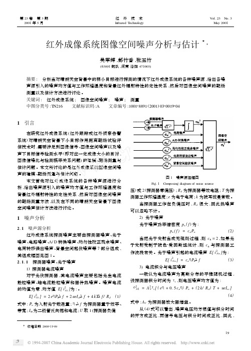
红外焦平面读出电路噪声分析
003-红外成像系统图像空间噪声分析与估计
式中 : L b 为探测波段内背景红外辐射亮度 。 2. 1. 5 电荷转移读出噪声 电荷转移读出噪声源主要有 4 个 ,1) 电荷转移损 失噪声 ,2) 背景电荷的引入噪声 ,3) 界面态俘获噪声 , 2 4) 光电子散粒噪声 。总噪声 σ N5为 :
2 2 ε σ N ( N s + N s0 ) + k TC/ e + N5 = 4 ( 8) 1 . 4 kTN ssN gA g / e + N s 式中 :ε为传输损失 ; N 、 N g 分别为转移次数及电极数
( 7)
0,
| ωx | Φ ωx0 | ωx | > ωx0
,
( 13)
2001 年 5 月 吴军辉等 : 红外成像系统图像空间噪声分析与估计 第 23 卷 第3期
S y ( t i ,ωy ) =
Ay ,
0,
| ωy | Φ ωy0 | ωy | > ωy0
第 23 卷 第3期 红 外 技 术 Vol. 23 No. 3 2001 年 5 月 Infrared Technology May 2001
红外成像系统图像空间噪声分析与估计 3
吴军辉 ,郜竹香 ,张玉竹
(63891 部队 ,河南 洛阳 471003)
对于热成像系统 , 电路噪声主要包括电压放大器 噪声 、 信号传输噪声以及干扰噪声 。电压放大器为有 源电路 ,其噪声源主要有热噪声和 PN 结散粒噪声 , 其 中热噪声与放大器工作温度有关 ,散粒噪声为一常数 ; 信号传输噪声以及干扰噪声都可以看成常数 。因此 , 可把电路噪声表示为 : 2 σ N 2 = cN 21 T + cN 20 式中 : T 为放大电路器件工作环境温度 。 当设备稳定工作时 , 放大器工作温度一般浮动范 围不大 ,因此 ,我们可以近似把电路噪声当成常量 , 与 红外成像系统工作环境温度无关 。
基于空时域级联滤波的红外焦平面条状噪声消除算法

基于空时域级联滤波的红外焦平面条状噪声消除算法王书朋;付程琳;侯颖【摘要】针对红外图像中的条状噪声问题,本文提出了一种基于空时级联滤波的条状噪声消除方法.在红外焦平面阵列中,每列设有一个读出电路用于读取该列传感器的响应.读出电路偏置电压的差异是红外图像中条状噪声的主要成因.根据红外辐射的空间相关性假设,本文利用空域非线性滤波从红外图像中提取偏置电压;然后,采用高斯-马尔科夫过程建立偏置电压随时间的变化的数学模型,并采用基于时域卡尔曼滤波的最小均方误差估计(MMSE)方法估计偏置电压;最后,从红外图像中减去偏置电压以消除红外图像中的条状噪声.为了验证所提算法的性能,分别利用仿真数据和实际红外数据进行实验,实验结果表明本文所提算法能够有效消除红外图像中的条纹噪声,并且不会造成图像细节的损失.【期刊名称】《红外技术》【年(卷),期】2018(040)004【总页数】5页(P377-381)【关键词】红外图像;条状噪声;空时级联滤波;红外焦平面阵列【作者】王书朋;付程琳;侯颖【作者单位】西安科技大学通信与信息工程学院,陕西西安 710054;西安科技大学通信与信息工程学院,陕西西安 710054;西安科技大学通信与信息工程学院,陕西西安 710054【正文语种】中文【中图分类】TN2160 引言红外成像系统在军事和民用方面都有广泛的应用,如夜视、监控、火灾检测等[1]。
红外成像系统的核心部件是红外焦平面阵列(IRFPA),它由许多位于透镜焦平面上的传感器组成,并使用读出电路读取传感器上的响应。
IRFPA中的每个读出电路只读取与其同列的传感器响应。
由于工艺水平限制,各列读出电路的电器特性无法做到完全相同,不同的读出电路会在原始的传感器响应上加入不同的偏置电压,这就导致红外图像上有明显的条状噪声[2-3]。
这类噪声严重影响了红外图像的质量,并且用传统的非均匀校正技术难以消除[4-5]。
此外,由于区分条状噪声与图像纹理非常困难,例如无法区分条状噪声和图像边缘,这就使得采用传统的图像去噪方法无法有效去除条状噪声,可能还会造成图像细节的损失[6]。
边积分边读出低噪声红外焦平面读出电路研究

红 外 与 毫 米 波 学 报
J nrr d Mii .Ifae l m.W a e l vs
Vo1 3 ,No 4 . 0 .
Au u t 2 g s , 01 1
cpc o 0 1 F nm d f n g t nw i ed h i ut a enf r a dwt . m 5V N w l C S aair( .5p )i o eo tr i hl ra .T ecr ih sbe bi t i 0 5 —e MO t ie ao e c ce h l
s n — — o ert ,an w c r l e o besmp n C S i ut s rsne r l n t gK C n i f ne ai i a t n i i e or a dd u l a l g( D )c c ii p ee tdf i a n T os o t t n gl o s a o et i r o e mi i e i g o r
f c d wih I a e t nGa e e t r . As d t co s
Ke o d :n a dfc ln r y F A) ra otn gae i ut R I ;ne a o hl ra ; o ea ddu - yw rs if e a paea a( P ; edu t rtdc ci ( O C) it t nw i d cr l e o b r r ol r ie r r g i ee t
Ch n s a e fS in e , h g a 2 0 8 C i a i e e Ac d my o ce c s S a h i 0 0 3, h n ; n
红外热像仪的空间噪声和时间噪声分析
红外热像仪的空间噪声和时间噪声分析马宁;刘莎;李江勇【摘要】噪声特性是衡量红外热像仪的一个重要指标.本文对热像仪的噪声来源和影响因素进行了分析,并通过实验分别计算了实测图像的空间噪声和时间噪声.实验结果表明了在实际观测过程中,图像的空间噪声通常要大于时间噪声,而且空间噪声在热像仪经过非均匀性校正之后的一段时间内会逐渐增大,而时间噪声不会有明显变化.基于时间噪声小于空间噪声且不随时间变化的特点,为红外图像中的目标检测提出了新的思路.%Noise characteristic is an important indicator for evaluating an infrared thermal imager.The sources and influence factors of noise were analyzed,and the spatial noise and temporal noise of the real images were calculated through the experiment.The results show that the spatial noise is usually greater than the temporal noise,and the spatial noise gradually increases after nonuniform correction of infrared thermal imager,while temporal noise has no obvious change.This characteristic provides new thoughts for target detection in infrared images.【期刊名称】《激光与红外》【年(卷),期】2017(047)006【总页数】5页(P717-721)【关键词】噪声;热像仪;红外;焦平面探测器【作者】马宁;刘莎;李江勇【作者单位】华北光电技术研究所,北京 100015;北京市复兴路14号80分队,北京100843;华北光电技术研究所,北京 100015【正文语种】中文【中图分类】TN219噪声特性是衡量红外热像仪的一个重要指标。
256×1长波红外焦平面器件低噪声信息获取电路研制
256×1长波红外焦平面器件低噪声信息获取电路研制姜婷;王淦泉;席红霞【摘要】According to 256×1 long-wave infrared focal plane array detector working principle and characteristics of the output signal, this paper elaborates LWIR detector information acquisition circuit design process from the perspective of low noise. The emphasis is to solve the problem of how to reduce the noise of the hardware circuit, and an accurate noise model is established. The experimental results show that the information acquisition circuit is in normal operation and the input noise of the whole circuit is 0.13mV, which has good noise characteristics.%针对256×1长波红外焦平面器件工作原理和输出信号特点,从低噪声需求角度出发,阐述了长波红外焦平面器件信息获取电路设计过程。
着重分析、并解决了信息获取电路如何降低硬件电路噪声问题,同时对硬件电路的噪声来源进行了分析与建模。
实验结果表明,信息获取电路正常工作,整个信息获取电路的输入均方根噪声为0.13 mV,具有良好的噪声特性。
【期刊名称】《红外技术》【年(卷),期】2016(038)005【总页数】6页(P378-383)【关键词】256×1;长波红外;信息获取电路;低噪声【作者】姜婷;王淦泉;席红霞【作者单位】中科院上海技术物理研究所,上海 200083; 中国科学院大学,北京100049;中科院上海技术物理研究所,上海 200083;中科院上海技术物理研究所,上海 200083【正文语种】中文【中图分类】TN215红外成像系统在航天、气象、医学、工业、安全等各个领域中有着广泛的需求,而长波红外成像技术对地和太空观测已经成为一个重要的发展方向[1-2]。
红外焦平面CTIA型读出电路的设计研究
红外焦平面CTIA型读出电路的设计研究蔡晶晶;刘晓东;张轩雄【摘要】In order to adapt to the trend of high pixel demand of infrared focal plane (IRFPA),it is necessary to design a smaller size and better performance pixel circuit.A capacitive transimpedance amplifier (CTIA) was selected as the circuit structure of the pixel circuit.The cascode structure was adopted for the CTIA,and the integration time was able to be adjusted by using the optional integrated capacitors.The pixel circuit was modified to reduce the area for meeting the need of high pixel.In addition,the analog signal chain was set up and analyzed by simulation.Its layout was drawn and then it was post simulated to provide a guarantee of accuracy and reliability of the readout circuit (ROIC).After optimization,the area of the pixel circuit is 18 μm × 18 μm,and the optional integrated capacitors are 60 fF and 400 fF respectively.The output swing of the analog signal chain is 2.03 V at room temperature and 1.52 V at lowtemperature,obtained in the postsimulation.The output integrated noise at low temperature is 213.6 μV,which is lower than the former structure,and can meet the requirements in the post-simulation.%为了适应红外焦平面(IRFPA)高像素的趋势,设计出面积更小、性能更优的像元电路,选择电容反馈跨阻放大器(CTIA)作为像元电路的电路结构,在CTIA中运算放大器基于共源共栅结构,采用积分电容可选的模式来调整积分时间,并基于电路高像素的需求,优化电路,减小面积.在此基础上,搭建模拟信号通路进行仿真研究,绘制版图,并进行后仿,为读出电路的正确性、可靠性提供保障.优化后的像元电路面积为18 μm×18μm,可选积分电容分别为60 fF和400 fF,后仿得到的信号通路输出摆幅常温下为2.03 V,低温下为1.52V,且低温下的积分噪声为213.6 μV,满足设计需求.【期刊名称】《上海理工大学学报》【年(卷),期】2017(039)004【总页数】7页(P346-352)【关键词】红外焦平面;读出电路;像元电路;CTIA;模拟信号通路【作者】蔡晶晶;刘晓东;张轩雄【作者单位】上海理工大学光电信息与计算机工程学院,上海200093;复旦大学微电子学院,上海201210;上海理工大学光电信息与计算机工程学院,上海200093【正文语种】中文【中图分类】TN432红外焦平面阵列属于红外光学系统,是一种红外成像器件,广泛用于军事领域、民事领域.红外焦平面阵列由红外探测器和读出电路两部分组成[1].红外探测器将红外辐射转换成电信号,读出电路对探测器输出的电信号积分采样,采样结果通过缓冲器串行读出.读出电路既有模拟电路又有数字电路,是典型的数模混合集成电路.其中模拟电路负责对探测器电流积分、采样和传输,并提供电路所需的偏置;数字电路产生控制时序,控制读出电路积分、采样的时间节点,并根据所设置的控制字,选择窗口大小、积分模式、输出通道个数等多种功能.其中,输入级电路作为读出电路的核心部分,其性能对读出电路的噪声、功耗、面积等参数有很大影响.目前,报道的输入级电路有多种结构[2],如SI (自积分)、SFD (源跟随器)、DI (直接注入)、GMI (电流镜栅调制)、BDI (缓冲直接注入)以及CTIA(电容反馈跨阻放大器)等.SI结构简单,占用面积少,但是输出无增益,需要后接电荷放大器,并且积分电容的非线性会引起输出的非线性.SFD结构简单,适用于大面积、低功耗的读出电路,在低背景下有较好的信噪比,但是其在中、高背景下,输出信号的非线性较为严重,并且源跟随器会引入较大的噪声.DI结构由注入管和积分电容构成,占用面积较小,但在低背景下,探测器光电流较小,使得注入管跨导变小,输入阻抗增大,注入效率降低,增大了电路的非线性度.GMI结构利用电流镜的复制作用,将光电流按比例放大或缩小,再进行积分.GMI相比DI有更高的灵敏度,但是GMI不能给探测器提供稳定的偏压.BDI结构是在DI结构基础上,跨接反相放大器,降低了电路的输入阻抗,提高了注入效率,改善了响应,但是面积与功耗都较大.CTIA结构虽然相较前面几种较为复杂,功耗较大,但是CTIA结构中运放与积分电容构成负反馈回路,可以提供很低的输入阻抗、较高的注入效率,能为探测器提供稳定的偏压.在从低到高的背景范围内,CTIA噪声都很小,非线性度低[3].综合考虑下,本文选取CTIA结构作为读出电路的输入级结构.传统的CTIA结构采用两级运算放大器结构,至少需要8个MOS管和一个比较大的补偿电容,占用面积大,功耗高[4].而现今,随着读出电路的规格越来越大,为了使读出电路达到百万像素,就需要增大读出电路的阵列规格,显然,如果采用传统的CTIA结构,那么读出电路的尺寸将会变大,不利于读出电路与其他模块的集成.因此,需要进一步减小像元电路的尺寸.本文采用一种基于共源共栅结构的CTIA电路[2,5],对CTIA 电路进行优化,根据电荷容量调整电容大小,采用积分电容可选的积分模式,并采用一位带宽控制结构,减小了电路面积,优化了电路功能,优化后的像元电路面积为18μm×18 μm,可选积分电容分别为60 fF和400 fF.另外,为确保电路功能的正确性,文中对读出电路的模拟信号通路进行分析研究,并在常温300 K和低温150 K下进行仿真分析,后仿得到CTIA电路在低温下积分电压为2.41 V,噪声为213.6 μV,信号通路低温下输出摆幅为1.52 V,通过后仿结果可知,电路低温下的输出摆幅需要在今后进一步优化.1.1 电容反馈跨阻放大器图1(见下页)为输入级电路的多种电路结构示意图.电路结构中的各项变量分别为:Ci 为积分电容;Vsh为采样控制信号;MUX为输出端;VSS为接地端;Vr为复位电压;Rd与Cd分别为二极管自身电阻与电容;Vb为偏置电压;Vsub为二极管的衬底电压;Vi为注入电压.其中,CTIA(电容反馈跨阻放大器)是由运算放大器和反馈积分电容构成的一种复位积分器,电路结构如图1(e)所示.积分电容位于放大器的反馈回路上,探测器的电流在反馈电容上积分,复位管将积分电容上的电荷放电,并将输出端复位至参考电平. CTIA选用共源共栅结构的运算放大器,并基于文献[2]中的电路结构进行优化.为减小单元电路面积,电路采用一位带宽控制,并调整电容大小及MOS管尺寸,CTIA电路如图2所示(见下页).图2中VDD为电源,bwl_b为带宽选择控制信号,lowg_b为积分电容选择信号,reset为复位信号,at_bloom为防溢出信号,r_sw为行选信号;Vso为采样输出信号,Ii为探测器输入电流,Vc为共源共栅结构中的偏置电压,Vo1为CTIA结构的输出电压,Vo2为像元电路中的输出电压.电路中积分电容越大,电荷容量越大,引入的噪声电子数也越大;而若积分电容太小,则会导致积分电压过高,非线性失真增加,因此在CTIA电路中采用积分电容可选的方式,由积分电容选择管实现.为了满足单元电荷容量0.3 Me,4 Me可选的指标要求,积分电容分别取值为C1=60 fF和C2=400 fF.当电容选择管栅端信号lowg_b为低电平时,积分电容为C1+C2;为高电平时,积分电容为C1.当复位管栅端信号reset为高时,探测器的电流在积分电容上开始积分;reset为低时,积分电容放电,CTIA单元输出端恢复至参考电平.当采样管栅端信号为低时,采样管导通,从CTIA输出端开始采样,采样结果输入由M9与M10构成的源极跟随器中,并传输到下一级缓冲器.出于面积以及噪声的考虑,电容C2受带宽选择管M4和积分电容选择管M5控制而分时复用,M4和M5不能同时导通.当带宽选择管导通时,会降低一些高频部分的噪声.本文采用一位带宽选择,以减少MOS管的KTC噪声,又保证了CTIA高频部分的降噪.CTIA的噪声对红外焦平面探测器微弱信号输出的信噪比有着重要的影响[6].电路中有两种噪声,分别为热噪声(KTC噪声)和闪烁噪声(1/f噪声).CTIA电路中带有复位开关,开关的打开和闭合都会产生KTC噪声.当开关断开时,噪声会随输入信号的瞬时值保存到积分采样电容上.KTC噪声是读出电路中起主要作用的噪声.闪烁噪声是MOS管在漏电流中产生的噪声.CTIA电路的总噪声是CTIA复位阶段的噪声与积分阶段的噪声之和,计算公式[7-8]为(Ci+gm,r)2+[8kTγ(+)++]式中:k是玻尔兹曼常数;T是温度;γ是体效应系数;KP是PMOS管的闪烁噪声系数;KN是NMOS管的闪烁噪声系数;COX是单位面积栅氧电容;gm是MOS管跨导;Ci是积分电容;W是MOS管栅宽;L是栅长;f是频率;Ri,a为放大器的输入电阻.从式(1)可以看出,当CTIA电路处于复位阶段时,积分电容越大,引入的噪声越大.因此,采用积分选择管是有意义的.1.2 模拟信号通路为了验证电路功能的正确性,将模拟信号通路提出,信号通路的结构如图3所示.最左侧为红外探测器,中间部分为CTIA型读出电路,最右侧为读出电路的缓冲电路,OUT 为输出端,电路中设计了三级缓冲.读出电路选用CTIA作为前级放大器,探测器电流在CTIA的反馈电容上积分,并由放大器进行采样、保持,由M9和M10构成的源极跟随器的输出端接入下一级缓冲器,最后通过多级缓冲器与跟随器输出.缓冲器一般输入电阻大,输出电阻小,常用的缓冲器有两种结构:源极跟随器和单位增益缓冲器.由图3可知,在信号通路中,CTIA单元电路后接多级缓冲器,且均为差分输入的单位增益缓冲器,与输出端相连的是跟随器电路.跟随器电路结构如图4所示,由差分放大器构成,负的输入一端与输出端相连,构成单位增益缓冲器,pd为上拉信号.跟随器比较重要的性能有驱动能力、跟随特性、稳定性等[8].输出摆幅反映跟随特性,它是使所有晶体管都工作在饱和区的输出电压的范围.如果输出电压过低,M4和M5工作在线性区;如果输出电压过高,M2工作在线性区.因此,跟随器的输出摆幅的计算公式为式中:VGST是过驱动电压.经计算可以得到摆幅为[0.3 V,3.2 V].动态范围是读出电路的一个重要的性能参数,定义为输出摆幅与输出噪声之比[9],计算公式为式中:Vsw是读出电路的输出摆幅,Voutrms是读出电路的输出积分噪声.动态范围反映了读出电路的信噪比,在实际电路中,需要根据探测器光电流的信号范围来确定读出电路的动态范围[3].红外焦平面的探测器采用光子型探测器.光子型探测器是一种基于光电效应的红外探测器,由于红外线的频率较低,所以探测器材料的禁带宽度必须足够小.常温下窄禁带半导体载流子的热激发会导致大量载流子从禁带跃迁到导带,会对电路造成干扰.因此,通常使探测器保持在低温下.电子系统在低温下有许多优点[10],例如迁移率增加,工作速度提高;互连线导电性提高,信号传输时间缩短;电路的开关速度、噪声容限以及增益带宽积都得到改善.低温特性在本文表现为噪声减小,延迟时间缩短,功耗降低等.因此,本文将比较常温300 K和低温150 K下CTIA电路的仿真结果,并加以分析.采用0.13 μm CIS工艺在Cadence Spectre软件下对CTIA及信号通路进行仿真.在常温300 K与低温150 K下分别对信号通路进行瞬态仿真,图5是常温下CTIA 的瞬态曲线,可以看出,当积分电容积分完成后,采样控制信号Vsh由高电平变为低电平,开始采样.图6(见下页)为不同输入电流下的瞬态曲线,探测器电流的改变不影响积分电压的大小,积分电压只与积分电容有关,同时探测器电流越大,放电越快.带宽选择管M4和积分电容选择管M5栅压的不同使得积分电容与带宽限制电容有三组取值,瞬态仿真曲线如图7所示(见下页).当积分电容选择管关断时,积分电容为C1,电容放电较为缓慢;当积分电容选择管导通时,积分电容为C1+C2,放电较快.从图7中还可以发现,当积分电容Ci相同时,带宽限制电容Cb的不同值不影响CTIA电路中积分电容的积分及复位.图8为300 K和150 K下的积分电压,可以看出,常温300 K时CTIA的积分范围为(0.38 V,2.74 V),150 K时积分范围为(0.21 V,2.52 V).以探测器电流取值1.5 nA为例,对CTIA电路和信号通路进行交流仿真,得到CTIA 的开环增益为110 dB,带宽为2.98 MHz.另外,为得出电路的等效输出噪声,对CTIA 及信号通路进行噪声分析.通过仿真分析可知,在输出噪声中热噪声起主导作用.在后面的定量分析中采用输出积分噪声作为衡量标准,积分噪声计算方法[11]为对CTIA和信号通路分别仿真噪声,计算输出积分噪声,得到的CTIA输出积分噪声见表1.信号通路在300 K下的输出积分噪声为408.7 μV,150 K下的输出积分噪声为317.6 μV.同时,根据式(1)估算出150 K下CTIA的输出积分噪声的理论值为236.33 μV,仿真结果与理论值的对比见表1.随后对缓冲器及跟随器分别进行直流扫描分析,以获取输出摆幅的大小.以图4的跟随器为例,将输入电压设置为变量,从0到3.3 V进行直流扫描分析,按照正负5 mV 的误差,得到输出摆幅,结果见表2.其他缓冲器的输出摆幅的仿真方法与跟随器一致.由于各缓冲器的MOS管参数不一致,三级缓冲器的输出摆幅均不相同.在信号通路中,信号需要通过多级缓冲器与跟随器,对信号通路进行仿真,按照正负误差10 mV,得到300 K下输出范围为(0.64 V,2.74 V),输出摆幅为2.10 V;150 K下输出范围为(0.77 V,3.14 V),由于150 K下电路积分电压是2.52 V,所以输出范围是(0.77 V,2.52 V),输出摆幅为1.75 V,数据如表2所示.从表2可以发现,通路的输出摆幅比单级缓冲器小,这是因为通路的负载阻抗比单级缓冲器大,拉低了输出摆幅.由式(3)计算可知,300 K时读出电路的动态范围是74 dB,150 K时的动态范围为74 dB.同时,根据前文得到的理论值计算可得,150 K时CTIA的动态范围是78.6 dB.比较可知,仿真的结果与理论值相差不大,满足设计要求.采用0.13 μm CIS工艺,在Virtuoso Layout XL中绘制CTIA电路及模拟信号通路的版图.CTIA单元电路的版图如图9所示,面积18 μm×18 μm.模拟信号通路的版图如图10所示,面积406.65 μm×57.26 μm.使用Calibre工具验证所绘版图,均通过 DRC与LVS检查.使用QRC提取版图的寄生参数,再利用所提取的参数进行后仿,得到如下结果:a. CTIA电路在300 K下积分范围为(0.42 V,2.64 V);150 K下积分范围为(0.28 V,2.41 V).b. 缓冲器、跟随器及信号通路的输出摆幅见表3,可以发现低温下输出摆幅变化较大.c. CTIA的输出积分噪声结果如表4所示,信号通路在300 K下的输出积分噪声是279.1 μV,在150 K下输出积分噪声为209.1 μV.从表1中可以看出,CTIA的输出积分噪声的理论值与前仿结果相差不大,后仿结果与之相比相差亦不大,符合电路的设计指标.现将仿真结果与文献[12]、文献[13]的结果进行比较,对比结果如表5所示,本文像元电路的尺寸为18 μm×18 μm,优于文献[12]与文献[13]的像元尺寸;输出摆幅占电源电压的比值为46%,优于文献[12]中的36%;以单个CTIA的功耗作为评判标准,本文中的CTIA的功耗优于文献[12],但劣于文献[13],有待提高.红外焦平面读出电路基于CTIA单元电路,采用共源共栅放大器结构,选择可选积分电容的积分模式,优化电路,减小单元电路面积.根据设计需求调整了积分电容的大小与CTIA电路结构,使得CTIA单元电路的面积达到18 μm×18 μm的要求.单元电路面积越小,相同面积下的像元数量就越多,因此适用于大面阵的读出电路.优化后CTIA电路150 K下的噪声为213.6 μV,输出摆幅为1.52 V (电源电压为3.3 V),满足设计需求.另搭建模拟信号通路,并对信号通路进行仿真,通过仿真可知信号通路输出积分噪声较小,150 K下输出积分噪声为209.1 μV,通过前、后仿的结果对比,可以发现低温下跟随器的输出摆幅前后有较大差别.对比发现,该电路像元尺寸明显优于之前所报道的文献.但是也需要注意到电路的输出摆幅与之相较也略有减小,电路噪声略有增大,需要在今后的研究中继续优化电路的摆幅与噪声问题.【相关文献】[1] ROGALSKI A,ANTOSZEWSKI J,FARAONE L.Third-generation infrared photodetector arrays[J].Journal of Applied Physics,2009,105:091101.[2] 沈科.基于CTIA的快照式红外读出电路研究[D].成都:电子科技大学,2009.[3] 郝立超.甚长波红外探测器信号读出电路结构研究[D].上海:中国科学院研究生院(上海技术物理研究所),2014.[4] 王霄,史泽林.CTIA型读出电路结构优化研究[J].微电子学与计算机,2014,31(11):64-68.[5] FLIR.ISC9809 low background 320 specification[Z].America:FLIR System,2002.[6] VERMEIREN J,VAN BOGGET U,VAN HOREBEEK G,et al.Low-noise,fast frame-rate InGaAs 320×256 FPA for hyperspectral applications[C]∥Processing of SPIE,Infrared Technology and Applications XXXV.Orlando:SPIE,2009.[7] 王攀,丁瑞军,叶振华.短波IRFPAs读出电路CTIA输入级的优化设计[J].激光与红外,2013,43(12):1363-1367.[8] JOHNSON J F,LOMHEIM T S.Focal-plane signal and noise model-CTIA ROIC[J].IEEE Transactions on Electron Devices,2009,56(11):2506-2515.[9] 关有光,周文超,田小强.探测器动态范围对光束质量β因子测量的影响分析[J].激光与光电子学进展,2011,48(7):070401.[10] 赵宏亮.基于红外成像系统的低温读出电路设计技术研究[D].天津:天津大学,2012.[11] RAZAVI B.Design of analog CMOS integrated circuits[M].CHEN G C,CHENG J,ZHANG R Z,译.Xi′an:Xi′an Jiaotong University Press,2003:192-194.[12] 翟永成,丁瑞军.320×256大电荷容量的长波红外读出电路结构设计[J].红外与激光工程,2016,45(9):73-78.[13] WANG G N,LU W G,LIU D H,et al.Column-level passive sample and column-shared active readout structure for high speed,low power ROIC[J].ElectronicsLetters,2015,51(5):390-392.。
翻译(红外焦平面阵列的CMOS的噪声分析)

红外焦平面阵列的CMOS的噪声分析读出集成电路林加木[1,2] 丁瑞军[1] 陈洪雷[1] 沈晓[1,2] 刘非[1,2]([1]中国科学院上海技术物理研究所,上海200083 [2]中国科学院研究生院,北京100039)摘要:随着红外焦平面探测器的发展,在红外焦平面阵列(红外焦平面)的CMOS的读出集成电路的内部噪音逐渐成为一个影响红外焦平面发展的重要因素。
这项工作是研究红外焦平面CMOS读出集成电路的内部噪声。
这项工作的动机主要是对读出集成电路的机制和内部噪声的影响分析。
并根据信在号传输过程中,对多种内部噪声进行分析。
根据理论分析的结果,表明1 / f噪声、KTC噪声和脉冲开关噪声在频域的幅度更大。
这些噪音已严重影响了输出信号的性能。
这项工作知道读出集成电路芯片的信号频率,这是使用DI读出模式的测试。
对频率测试结果进行分析后,显示1 / f噪声和脉冲开关噪声是红外焦平面CMOS读出集成电路的内部噪声的主要组成部分,它们的噪音使输出信号产生重大影响。
根据噪声类型,提出一些噪声抑制的方法。
之后,这些方法用EDA软件进行仿真,结果表明,噪音减少。
这项工作的研究结果为提高红外焦平面CMOS读出集成电路的噪声抑制设计提供了参考依据。
关键词:红外焦平面阵列,读出集成电路,噪音,频谱分析1 引言在红外信号检测应用中,检测到内部噪声严重地限制了红外焦平面阵列(红外焦平面)的红外辐射信号的能力。
无法避免的内部噪声,必须抑制或减少,以提高输出信号的信噪比(S / N)[1,2]。
红外焦平面的噪声可能来自外面的世界,也可能来自红外探测器和读出集成电路(ROIC)本身。
,我们必须分析噪声来源,以采取有效的方法来抑制或降低噪音的强度和破坏。
这是读出电路设计的重点和难点。
部分的红外焦平面CMOS读出电路的噪音可能来自使用设备的基本物理过程中,有些是由于材料和制造过程中的偏差。
还有一些噪音是由于电路结构和读出集成电路的工作方法[3]。
320×256中波红外焦平面器件低噪声采集系统设计
320×256中波红外焦平面器件低噪声采集系统设计李锋;董峰;冯旗【摘要】根据320×256中波红外焦平面器件内部电路结构特点以及输出微弱模拟信号的特点,系统从低噪声和抗干扰的角度出发,设计了由电源模块、驱动电路、A/D转换电路、数据处理电路、时序控制模块等模块组成的低噪声中波红外焦平面图像数据采集系统.通过噪声测试和成像实验得到,在26℃的室温下,测得的电路噪声为0.1 mV,在1000μs积分时间时系统噪声1.5 mV,各个像元的SNR在62~65 dB之间.%This paper provides a description of the signal processing design procedure for an acquisition system with low noise, using the internal circuit structure characteristics and output analog signal characteristics of a 320×256 medium wavelength infrared FPA. A medium wavelength infrared FPA image data acquisition system consists of a power supply module, drive circuit, A/D conversion circuit, data processing circuit, and sequential control module. Through noise tests and imaging experiments, the circuit's noise is found to be approximately 0.1mV and the system's noise is approximately 1.5mV at 26℃(room temperature). A pixel's signal-to-noise ratio (SNR) is between 62dB and 65dB. The results show that the system has good noise characteristics and that it can meet the requirements of practical engineering applications.【期刊名称】《红外技术》【年(卷),期】2017(039)008【总页数】6页(P704-709)【关键词】320×256焦平面;中波红外;低噪声;采集系统【作者】李锋;董峰;冯旗【作者单位】中国科学院大学,北京 100049;中国科学院上海技术物理研究所,上海200083;中国科学院红外探测与成像技术重点实验室,上海 200083;中国科学院上海技术物理研究所,上海 200083;中国科学院红外探测与成像技术重点实验室,上海200083;中国科学院上海技术物理研究所,上海 200083;中国科学院红外探测与成像技术重点实验室,上海 200083【正文语种】中文【中图分类】TN215红外探测器能够把对目标接收到的红外辐射信息转换成一种便于计量的物理量,通常是电量即电信号,然后利用外围读出电路对电信号经过采集、滤波、放大、降噪、模数转换等处理后获得被探测目标以及背景的图像信息[1]。
- 1、下载文档前请自行甄别文档内容的完整性,平台不提供额外的编辑、内容补充、找答案等附加服务。
- 2、"仅部分预览"的文档,不可在线预览部分如存在完整性等问题,可反馈申请退款(可完整预览的文档不适用该条件!)。
- 3、如文档侵犯您的权益,请联系客服反馈,我们会尽快为您处理(人工客服工作时间:9:00-18:30)。
Design of 800×2 Low-Noise Readout Circuit for Near-InfraredInGaAs Focal Plane ArrayHuang Zhangcheng*a, Huang Songlei a, Fang Jiaxiong aa State Key Laboratory of Transducer Technology, Shanghai Institute of Technical Physics, ChineseAcademy of Sciences, Shanghai 200083, ChinaABSTRACTInGaAs near-infrared (NIR) focal plane arrays (FPA) have important applications in space remote sensing. A design of 800×2 low-noise readout integrated circuit (T800 ROIC) with a pitch of 25 µm is presented for a dual-band monolithic InGaAs FPA. Mathematical analysis and transient noise simulations have been presented for predicting and lowering the noise in T800 ROIC. Thermal noise from input-stage amplifier which plays a dominant role in ROIC is reduced by increasing load capacitor under tradeoff and a low input offset voltage in the range of ±5 mV is obtained by optimizing transistors in the input-stage amplifier. T800 ROIC has been fabricated with 0.5-µm 5V mixed signal CMOS process and interfaced with InGaAs detector arrays. Test results show that ROIC noise is around 90 μV and input offset voltage shows a good correspondence with simulation results. 800×2 InGaAs FPA has a peak detectivity (D*)of about 1.1×10¹² cmHz1/2/ W, with dynamic range of above 80dB.Keywords: infrared FPA, ROIC, low noise, input offset voltageINTRODUCTIONInGaAs near-infrared focal plane array has wide applications in space remote sensing, NIR spectroscopy and night vision [1][2]. As InGaAs detector has a high detectivity from 0.9 μm to 1.7 μm at room temperature with its lattice matched to InP substrate, there has been strong interest in developing InGaAs FPA as optoelectronic sensor for remote sensing [3]. In general, InGaAs FPA consists of two major parts, namely InGaAs detector arrays and the readout integrated circuit. In the past years, the advances of detector fabrication technology have led to the rapid development of InGaAs detector array [4]. At present, for many mature InGaAs FPA detector technologies, it is the readout electronics that limit performance rather than the detector itself.In this paper, a design of low-noise 800×2 CMOS ROIC for near-infrared InGaAs focal plane array is presented. The first section describes basic architecture of ROIC. The second section presents a mathematical analysis of total noise and the design method of low-noise ROIC circuit. To obtain low dark current in FPA, the next section discusses the input offset voltage of input amplifier. The last section will present performance measurements and comparison with calculation results.800×2 ROIC ARCHITECTUREInGaAs near-infrared focal plane array has been studied in Shanghai Institute of Technical Physics (SITP) for several years [5][6]. Now there is a great interest in developing an 800×2 InGaAs NIR focal plane array for dual-band detection. This paper reports the development of 800×2 low-noise ROIC (T800) suitable for dual-band monolithic InGaAs detector arrays.T800 ROIC consists of two parallel 800×1 linear arrays with 25µm pixel pitch. Figure 1 shows the architecture of unit circuit in T800 ROIC.Infrared, Millimeter-Wave, and Terahertz Technologies II, edited by Cunlin Zhang, Xi-Cheng Zhang, He Li, Sheng-Cai Shi, Proc. of SPIE Vol. 8562, 856205 · © 2012 SPIE · CCC code: 0277-786/12/$18 · doi: 10.1117/12.999646Figure 1. Architecture of unit circuit in T800 ROICThe input stage of unit circuit is based on capacitive-feedback transimpedance amplifier (CTIA), which interfaces the InGaAs pixel and performs current-to-voltage conversion. It consists of an operational transimpedance amplifier (OTA) with a capacitor (C int) connected in feedback loop. High ratio of current-to-voltage can be achieved if the integration capacitor is small; however it leads a low dynamic range as the full well capacity directly scales with integration capacitor. For our design we chose an integration capacitor of 0.5 pF for the high dynamic range need of the application. It is necessary to consider how to realize low-noise performance in the design trade-off of a high-dynamic-range ROIC pixel. The load capacitor (C L) is added at output node of OTA to reduce the input stage noise by lowering the close loop bandwidth of CTIA, meanwhile, Correlated Double Sampling (CDS) is used to remove KTC noise and reduce the low-frequency noise from InGaAs detector and input stage amplifier. By CDS, T800 reads pixel signal two times – once at the beginning of the integration time, and another at the end. Effective signal is obtained by subtraction of the two samples. At the output stage, source follower is involved to transfer parallel to serial and drive the bus.NOISE ANALYSIS AND OPTIMIZATIONIn low-noise design, a careful analysis of each noise source is necessary. In InGaAs FPA, typical noise mechanisms include InGaAs detector thermal noise, shot noise, CTIA KTC noise, amplifier thermal noise, 1/f noise, KTC noise from sample circuit, SF output stage noise, and so on.The detector thermal noise σTH and shot noise σDK (from dark current) can be given [7]:/ TH qσ= (1)DKσ= (2)where R det is detector resistance, t int is integration time, I DK is dark current, T is temperature, and k is the Boltzmann constant.When CTIA starts working in integration mode, the noise from last reset mode will be added in integration voltage at the beginning. The CTIA KTC noise, σRST, consists of two terms: one comes from reset switch and another originates from the amplifier noise, which can be given [8]:/ RST qσ= (3) where C tot = C int + C det +C L, α = 2(1+g m7/g m1)/3, C det is detector capacitor, g m1 and g m7 are transconductance of input transistor and load transistor in OTA respectively.Mostly the thermal noise of CTIA amplifier is one of the dominant noise sources in the circuit. The small signal equivalent circuit for OTA thermal noise analysis is shown in Figure 2.Figure 2. Small signal equivalent circuit for OTA thermal noise analysisThe transfer function from the amplifier noise current to output voltage isdet intint()o a a x m v C C H s i C s g C +==+ (4) where C x = C int C det + C det C L + C L C int , g m is transconductance of OTA.The one-sided noise current power spectral density (PSD) in units (A 2/Hz) from differential amplifier is()8a m S f kTg α= (5)The equivalent input noise in units (e-) can be written:AMPσ==The S &H noise, σSH, can be given:SH σ=(7) where C SH is sample capacitor.And the noise from SF output stage:SF σ=(8)CTIA KTC noise σRST and low-frequency (smaller than 1/t int ) 1/f noise can be greatly cancelled by CDS, however, CDS will increase the thermal noise from CTIA OTA by a square root of two because of double samples. The OTA thermalnoise after CDS in units (e-) can be written:,AMP CDS σ=Table 1 summarizes the expressions and calculation results of noise in T800 ROIC and 800×2 InGaAs NIR FPA. As shown in table 1, noise level in ROIC after CDS is 331 e- which is better than noise level (488 e-) without CDS. The OTA thermal noise plays a dominant role in whole ROIC noise mechanisms.Equation 7 and 9 show that ROIC noise can be reduced by increasing load capacitor C L and sample capacitor, C SH , however, this also increase the layout area of unit circuit. It is necessary to compare ROIC noise to InGaAs noise, for it is useless to lower FPA noise with load capacitor increment if the global FPA noise performance is limited by detectors [9].①The value of C L and C SH are specified when ROIC noise power is a half of InGaAs detector noise power. Transient noisesimulation results of T800 ROIC versus C L and C SH are shown in Fig 3. T800 ROIC noise is less than 320 e- if we choose C L = 3 pF, C SH = 2 pF. Results of 800 transient noise simulations are shown in Fig 4. The standard deviation is found to be 321 e-, which approaches the calculation results.P o p u l a t i o nROIC Noise (e -)Figure 3. ROIC noise simulation results vs. C L , C SH Figure 4. Histogram of ROIC noise simulation resultsINPUT OFFSET VOLTAGE ANALYSISAnother key element is dark current in FPA. Low dark current is needed for lowering shot noise from dark current and fixed pattern noise. Under a simplifying assumption, the detector resistance near zero-bias is invariable. The dark current in InGaAs FPA can be given as:det /DK os I V R = (10)where V os is input offset voltage of CTIA OTA.For FPA, it is useful to achieve small dark current by reducing V os in CTIA OTA [10]. The architecture of CTIA OTA is shown in Fig 5.Figure 5. CTIA OTAV os is determined primarily by input transistor (M1, M2)and load transistor (M7, M8), which is given as:,,771,,,117(/)(/)2(/)2(/)GS TH N GS TH P m os inTH P TH N m V V V V g W L W L V V V W L W L g ⎧⎫⎧⎫−−⎡⎤⎡⎤ΔΔ⎪⎪⎪⎪=+Δ++Δ⎨⎬⎨⎬⎢⎥⎢⎥⎣⎦⎣⎦⎪⎪⎪⎪⎩⎭⎩⎭ (11) ΔV TH,P and ΔV TH,N will be greatly reduced if the layout of transistors using multiple fingers are perfectly symmetrical,then the next approach is to specify (W/L)1 and (W/L)7. Monte Carlo simulation results of V os versus (W/L)1 are illustrated in Fig 6. The standard deviation of V os is about 5mV when (W/L)1 = 10 and (W/L)7 = 4, and the increment improvement in V os decreases slightly for larger (W/L)1 and (W/L)7. Results of 800 Mento Carlo simulations are shown in Fig 7. Substituting simulation results of V os into Eq. (10) gives I DK ≈ 0.67 pA.V o s (m V )(W/L)1P o p u l a t i o nVos (mV)Figure 6. V os simulation results vs. (W/L)1 Figure 7. Histogram of V os simulation resultsMEASUREMENTST800 ROIC is fabricated using a 5 V 0.5-μm CMOS technology, which measures 21.2 mm × 6.1 mm of one die. The measured T800 ROIC and FPA performances are summarized in table 2.Noise measurements were conducted by sampling 100 consecutive frames and performing standard deviation calculation for each pixel. The ROIC noise is 352 e- which is slightly more than results of mathematical calculation (331 e-) and transient noise simulations (321 e-). Additional noise may originate from bias voltage and clocks. The dynamic range of 800×2 InGaAs FPA is above 80 dB, and peak detectivity is about 1.1×10¹² cmHz 1/2/ W. These attributes result in a high image quality for remote sensing.Table 2. T800 ROIC MeasurementParameter Typical Value Comments Array Format 800×2Pixel Pitch 25 μmROIC Noise 352 e- / 90 μV rms@25℃ FPA Noise 586 e- / 150 μV rms@5ms, 25℃ Full Well Capacity 6,640,000 e- Power Consumption 36 mW Dynamic Range 81 dB InGaAs FPA@5ms, 25℃Peak Detectivity 1.1×10¹²cmHz 1/2/ W @5 ms, 25℃ Non-Linearity <5% Dark Current -0.6 pA ∼0.6 pA FPA@25℃FPA Noise measurements and calculated results versus integration time are plotted in Fig 8. The measurement resultsperformed shows an approximate correspondence with theoretic analysis. Dark current distribution of measurements is shown in Fig 9. Dark currents in 800×2 InGaAs FPA are measured to be in the range of ±0.6 pA at 25℃, which coinciding well with calculation results. Dark current tests show that V os of CTIA OTA is about in the range of ±5 mVP o p u l a t i o nDark Current /pAFigure 8 Comparison of tests and calculations Figure 9 Histogram of I DK test resultsCONCLUSIONSA 25 μm pixel-pitch, 800×2 CTIA ROIC (T800) for a dual-band monolithic InGaAs FPA has been developed.Mathematical analysis and transient noise simulations have been presented for predicting and lowering the noise in T800 ROIC. Its pixel has a full-well-capacity of about 6,640,000 e- with an input referred read noise of 352 e-. The T800 ROIC runs on 5 V supply voltage and dissipates about 36 mW. Input offset voltage has been limited in the range of ±5 mV to decrease the dark current in InGaAs FPA. It has been fabricated using a 0.5-μm CMOS process and interfaced with InGaAs detector arrays. Due to low-noise and low-input-offset performance of ROIC, InGaAs FPA has a peak detectivity of about 1.1×10¹² cmHz 1/2/ W, with dynamic range of above 80 dB.REFERENCES[1] MacDougal, M H., Geske, J, "Low dark current InGaAs detector arrays for night vision and astronomy, "Proc. SPIE 7298, 72983F (2009).[2] Andrew D. Hood, Michael H. MacDougal, "Large-format InGaAs Focal Plane Arrays for SWIR Imaging, "Proc. SPIE 8353, 83530A (2012).[3]Jean-Luc Reverchon, Jean Decobert, "High dynamic solutions for short-wavelength infrared imaging based onInGaAs" Optical Engineering. Papers 50(6), 061014 (2011).[4]John A. Trezza, Navneet Masaun, "Analytic Modeling and Explanation of Ultra-Low Noise in Dense SWIRDetector Arrays," Proc. SPIE 8012, 80121Y (2011).[5]Gong Haimei, Tang Hengjing, Li Xue, "Near-infrared InGaAs FPAs for space application," Infrared andLaser Engineering. Papers 38(4), 574-582 (2009).[6]Huang Zhangcheng, Huang Songlei, Zhang Wei, "Low noise readout circuit for infrared focal plane array inintegration while read," J. Infrared Millim. Waves. Papers 30(4), 297-304 (2011).[7]Jerris F. Johnson, Terrence S. Lomheim, "Focal-Plane Signal and Noise Model–CTIA ROIC," IEEETRANSACTIONS ON ELECTRON DEVICES. Papers 56(11), 2506-1515 (2011).[8] A. Van Blerkom, "Analysis and Simulation of CTIA-based Pixel Reset Noise," Proc. SPIE 8012, 80120G(2011).[9]Eric de Borniol, Fabrice Guellec, "High-performance 640 × 512 pixel hybrid InGaAs image sensor for nightvision," Proc. SPIE 8353, 835307 (2012).[10]Douglas S. Malchow, Robert M. Brubaker, "Development of linear array ROIC for InGaAs detector arrays withwavelength response to 2.5 microns for NIR spectroscopy and machine vision," Proc. SPIE 6940, 69402V (2008).。