数字计时器
H5CR多功能数字计时器说明书
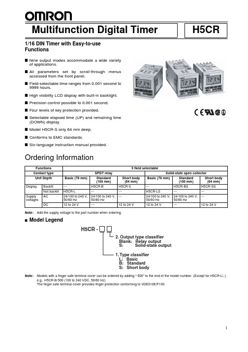
H5CRMultifunction Digital Timer1/16 DIN Timer with Easy-to-use FunctionsI Nine output modes accommodate a wide varietyof applications.I All parameters set by scroll-through menusaccessed from the front panel.I Field-selectable time ranges from 0.001 second to 9999 hours.I High visibility LCD display with built-in backlight.I Precision control possible to 0.001 second.I Four levels of key protection provided.I Selectable elapsed time (UP) and remaining time(DOWN) display.I Model H5CR-S only 64 mm deep.I Conforms to EMC standards.ISix-language instruction manual provided.Ordering InformationNote:Add the supply voltage to the part number when ordering.IModel LegendNote:Models with a finger safe terminal cover can be ordered by adding “-500” to the end of the model number. (Except for H5CR-L #)e.g., H5CR-B-500 (100 to 240 VDC, 50/60 Hz)The finger safe terminal cover provides finger protection conforming to VDE0106/P100.RC+Functions 9 field selectableContact type SPDT relay Solid-state open collectorUnit Depth Basic (78 mm)Standard (100mm)Short body (64mm)Basic (78 mm)Standard (100mm)Short body (64mm)Display Backlit ---H5CR-B H5CR-S---H5CR-BS H5CR-SSNot backlit H5CR-L------H5CR-LS------Supply voltagesAC 24/100 to 240V, 50/60 Hz 24/100 to 240V, 50/60 Hz ---24/100 to 240V, 50/60 Hz 24/100 to 240V, 50/60 Hz ---DC12 to 24 V---12 to 24 V12 to 24 V---12 to 24 VIAccessories (Order Separately)Note:1.Y92A-48G is a finger safe terminal cover which is attached to the P3G-08 Socket.2.Supplied with each Unit.SpecificationsNameModelHard cover Y92A-48Soft coverY92A-48F1Track Mounting/Front Connecting Socket (for H5CR-L # only)---P2CF-08Finger safe type P2CF-08-E Back Connecting Socket (for H5CR-L # only)---P3G-08Finger safe typeP3G-08 with Y92A-48G (see note 1)Finger Safe Terminal Cover for H5CR-B #/-S #Y92A-48T Flush Mounting Adapter (see note 2)Y92F-30ModelH5CR-L (Basic type)H5CR-B (Standard type)H5CR-S (Short body type)Classification Digital timerMountingFlush or Surface mounting Flush mountingExternal connections 8P socket Screw terminals (M3.5 screw)Enclosure ratings IP40IP54 (panel surface)Display modes Elapsed time (UP), remaining time (DOWN)Output modes A, A-1, A-2, A-3, b, b-1, d, E, FReset system Power reset (except A-3, b-1, and F modes), External, manual, automatic resets (internal according to A-1, b, b-1, d, and E mode operation)Input signals Start, reset inputsStart, reset, gate, key protect inputsInput method No-voltage input: Via opening and closing of contactControl outputs SPDT contact output and transistor output (NPN open collector)Display LCD without backlight LCD with backlight Digits4 digitsMax. time settings 9.999 s (0.001 s units), 99.99 s (0.01 s units), 999.9 s (0.1 s unit), 9999 s (1 s unit), 99 min 59 s (1 s unit), 999.9 min (0.1 min unit), 9999 min (1 min unit), 99 hr 59 min (1 min unit), 999.9 hr (0.1 hr unit), 9999 hr (1 hr unit)Memory backup Backup time for power interruption: Approx. 10 years at 20 C Mounting method DIN track mounting, surface mounting, and flush mounting Flush mounting Approved standardsUL508, CSA C22.2 No. 14Conforms to EN61010-1IRatingsICharacteristicsModelH5CR-L (Basic type)H5CR-B (Standard type)H5CR-S (Short body type)Rated supply voltage100 to 240 VAC (50/60 Hz)24 VAC (50/60 Hz)12 to 24 VDC (permissible ripple: 20% max.)100 to 240 VAC (50/60 Hz)24 VAC (50/60 Hz)12 to 24 VDC (permissible ripple: 20% max.)Operating voltage range 85% to 110% of rated voltagePower consumption Approx. 3 VA at 50 Hz, 240 VAC; approx. 1 W at 24 VDCApprox. 5 VA at 50 Hz, 240 VAC Approx. 2 W at 24 VDCReset and control signals Min. pulse width 1 ms/20ms selectable Gate ---Min. pulse width: Approx. 20 ms Key protect ---Response time: 1 sOne-shot time0.1 to 20 s (select from 7 kinds) or sustainedPower reset (except A-3, b-1, and F mode)Min. power opening time: 0.5 s Signal, reset, gate inputsNo-voltage input ON impedance: 1 k W max. (Approx. 2 mA when 0 W )ON residual voltage:2 V max.OFF impedance:100 k W min.Key protect input---No-voltage inputON impedance: 1 k W max. (Approx. 2 mA when 0 W )ON residual voltage:1 V max.OFF impedance:100 k W min.Control outputs Contacts: 5 A at 250 VAC, resistance load (cos f = 1)Transistor output: Open collector 100mA at 30 VDC max. residual voltage 2 V max. (Approx. 1 V)Ambient temperature –10 C to 55 C (with no icing)Storage temperature –25 C to 65 C (with no icing)Ambient humidity 35% to 85%Case Light grayRepeat accuracy (including temperature and voltage effects)Power start: 0.01% 0.05 s max.Control signal start: 0.005% 0.03 s max. *(rate for set value)Insulation resistance 100 M W min. (at 500 VDC) (between current-carrying terminal and exposed non-current-carrying metal parts, and between non-continuous contacts)Dielectric strength 2,000 VAC, 50/60 Hz for 1 min (between current-carrying terminal and exposed non-current-carrying metal parts) for 100 to 240 VAC type 1,000 VAC for 24VAC/12 to 24 VDC transistor output typeSurge voltage3 kV (between power terminals) for 100 to 240 VAC type, 1 kV for 24 VAC/12 to 24 VDC type4.5 kV (between current-carrying terminal and exposed non-current-carrying metal parts) for 100 to 240 VAC type, 1.5 kV for 24 VAC/12 to 24 VDC typeNoise immunity 2 kV (between power terminals)( 480 V for 12 to 24 VDC) and 600 V (between input terminals), square-wave noise by noise simulator (pulse width: 100 ns/1 m s, 1-ns rise)Static immunity Malfunction: 8 kV; destruction: 15 kVVibration Destruction 10 to 55 Hz with 0.75-mm single amplitude each in three directions Malfunction 10 to 55 Hz with 0.5-mm single amplitude each in three directions ShockDestruction 294 m/s 2 (30G) each in three directions Malfunction98 m/s 2 (10G) each in three directions Life expectancy Mechanical 10 million operations min.Electrical100,000 operations min. (5 A at 250 VAC in load resistance)EMC(EMI):EN50081-2Emission Enclosure:EN55011 Group 1 class A Emission AC Mains:EN55011 Group 1 class A (EMS):EN50082-2Immunity ESD:EN61000-4-2: 4 kV contact discharge (level 2)8 kV air discharge (level 3)Immunity RF-interference:ENV50140:10 V/m (80 MHz to 1 GHz) (level 3)Immunity Conducted Disturbance:ENV50141:10 V (0.15 to 80 MHz) (level 3)Immunity Burst:EN61000-4-4: 2 kV power-line (level 3)2 kV I/O signal-line (level 4)WeightH5CR-L: Approx. 105 g, H5CR-B: Approx. 160 g, H5CR-S: Approx. 120 gNomenclatureIFactory SettingsThe following table shows the timer settings when it is shipped. Please change the settings as necessary to suit the system before opera-tion. Settings and the display receive power from the internal battery and are therefore unaffected by external power interruptions.Note:With the initial settings, there will be no output even if the power supply is connected. External inputs and outputs cannot be used without a power supply.1213Model H5CR-B (Standard)/H5CR-S (Short body)H5CR-L (Basic)Time range - -. - -s Present value 0.00 s Presets0.00 s UP/DOWN mode UPOutput mode A: Signal on delay (I)Output time Sustained Input signal time 20 ms Key protect level KP-1---OperationI Block DiagramI I/O FunctionsInputs Start signal Stops timing in A-2 and A-3 (power on delay) modes. Starts timing in other modes.Reset Resets present value (to zero in UP modes, to preset in DOWN mode).Count inputs are not accepted while reset input is ON.Reset indicator lit while reset input is ON.Gate Inhibits timer operation.Key protect Makes keys inoperative according to key protect level.Key protected indicator lit while key protect input is ON.Effective when power supply is turned off.Effective when protect terminals are shorted.Outputs Control output (OUT)Outputs made according to designated output mode when corresponding preset is reached.I Operational OverviewThis flowchart shows operation common to all H5CR models. Refer to the following Setting Item Table for details on the operation of specific models.I Setting Item TableNote: 1.Changes made in setting mode become effective when run mode is entered.2.The time range setting appears first when setting mode is entered.3.*The key protection function is not included in the H5CR-L.<KP-4><KP-3>I ExamplesRun ModeChanging the Set ValueT o change the set value from 3 hr 5 min to 4 hr 5 min, press the 3key so that the number 4 appears in the hour’s place.•Pressing keys 1 through 4 increments the corresponding col-umn by 1.•The columns can be changed in any order, but the output willbe turned ON if the set value is less than the present value.•Nonsignificant zeros are suppressed on the set value display.Note:Read Changing Set Values in the Precautions section,page16, before changing the Timer set value during op-eration.Setting ModeChanging Settings in the Set Mode1.Press the MODE key to switch from run mode to set mode.•The Timer will continue operation if switched from run mode to set mode during operation.•The MODE key will be locked if the key protection function is enabled.•Settings changed in the set mode are not effective until run mode is entered. As the operating conditions will change in this case, always reset operation with the RESET key or a re-set input.2.Press the MODE key to scroll successively through the items that can be set.3.Changing the selected item•Press the MODE key until the desired item appears.•Change the item setting by pressing keys 1 through 4. (Pressthe DISPLAY key to switch back from set mode to run mode.)ITiming ChartsThe gate input is not included in the H5CR-L.Output mode A: Signal ON delay 1 (Timer resets when power comes ON.)Output mode A-1: Signal ON delay 2 (Timer resets when power comes ON.)Output mode A-2: Power ON delay 1 (Timer resets when power comes ON.)Output mode A-3: Power ON delay 2 (Timer does not reset when power comes ON.)Power Start signalGate ResetControl outputSet valueTiming diagramUPDOWNSet valueTiming starts when the start signal goes ON.While the start signal is ON, the timer starts when the power comes ON or when the reset input goes OFF .The control output is controlled using a sustained or one-shot time period.Basic OperationPower**Start signal inputTimingOutput* Output is instantaneous when setting is 0.** Start signal input is disabled during timing.Power Start signalGate ResetControl outputSet valueTiming diagramUPDOWNSet valueTiming starts when the start signal goes ON, and is reset when the start signal goes OFF .While the start signal is ON, the timer starts when the power comes ON or when the reset input goes OFF .The control output is controlled using a sustained or one-shot time period.*Output is instantaneous when setting is 0.Basic OperationPower Start signal inputTimingOutputPower Start signalGate ResetControl outputSet valueTiming diagramUPDOWNSet valueTiming starts when the reset input goes OFF .The start signal disables the timing function (i.e., same function as the gate input).The control output is controlled using a sustained or one-shot time period.*Output is instantaneous when setting is 0.Basic OperationPower TimingOutputPower Start signalGate ResetControl outputSet valueTiming diagramUP DOWNSet valueTiming starts when the reset input goes OFF .The start signal disables the timing function (i.e., same function as the gate input).The control output is controlled using a sustained or one-shot time period.*Output is instantaneous when setting is 0.Basic OperationPower TimingOutputSustainedOutput mode b-1: Repeat cycle 2 (Timer does not reset when power comes ON.)Power Start signalGate ResetControl output* Normal output operation will not be possible if the set time is too short.Set the value to at least 100 ms (contact output ** Start signal input is disabled during timing.TimingTiming Timing Timing Timing starts when the start signal goes ON.The control output is turned ON when time is up.While the start signal is ON, the timer starts when the power comes ON or when the reset input goes OFF .* Normal output operation will not be possible if the set time is too short.Set the value to at least 100 ms (contact output ** Start signal input is disabled during timing.Basic OperationPower Start signal OutputTimingTiming Timing Timing Timing starts when the start signal goes ON.The status of the control output is reversed when time is up (OFF at start).While the start signal is ON, the timer starts when the power comes ON or when the reset input goes OFF .* Normal output operation will not be possible if the set time is too short.Set the value to at least 100 ms (contact output ** Start signal input is disabled during timing.Sustained Basic OperationStart signal TimingTimingTiming starts when the start signal goes ON.The control output comes ON when time is up.While the start signal is ON, the timer starts when power comes ON or when the reset input goes OFF .Basic OperationStart signal * Normal output operation will not be possible if the set time is too short.Set the value to at least 100 ms (contact output ** Start signal input is disabled during timing.Sustained TimingTimingNote:A twin timer can be created by using one of the repeat modes. For example, if the set value is 60 s and the one shot time is 10 s in repeat mode, the control output will turn OFF for 50 s and ON for 10 s. (In the first cycle, however, the control output will turn OFF for 60 s.) In this way, the work of two timers can be performed by a single timer.Output mode E: Interval (Timer resets when power comes ON.)Output mode F: Cumulative (Timer does not reset when power comes ON.)* Output functions only during start signal input when setting is 0.** Start signal input is enabled during timing.Power Start signal OutputTimingTiming starts when the start signal comes ON.The control output is reset when time is up.While the start signal is ON, the timer starts when power comes ON or when the reset input goes OFF .* Output is disabled when the setting is 0.** Start signal input is disabled during timing.Basic OperationPower Start signal OutputTimingStart signal enables timing (timing is stopped when the start signal is OFF or when the power is OFF).A sustained control output is used.* Output is instantaneous when setting is 0.SustainedBasic OperationPower Start signal OutputTimingTiming10 s50 s 60 sDimensionsNote:All units are in millimeters unless otherwise indicated.484884.063.760.714.344.8 x 44.8 484866444.8 x 44.8H5CR-LSurface/Flush Mounting H5CR-BFlush MountingH5CR-S Flush Mounting4848100644.8 x 44.8IDimensions with Y92F-30 Flush Mounting Adapter4858685.95848610092.8AH5CR-BH5CR-SPanel CutoutsPanel cutouts areas shown below.(according to DIN43700).Y92F-30Flush mounting adapterPanel Y92F-30Flush mounting adapterPanel Note 1. The mounting panel thicknessshould be 1 to 4 mm.2. It is possible to mount timers side by side, but only horizontally.H5CR-LP2CF-08584866460 min.60 min.45+0.6-045+0.6-0+10A = {48n - 2.5 + (n -1) x 4}Panel Flush mountingadapter P3G-08Rear surfaceconnection socket44.8 x 44.8With Y92A-48F1 attached.44.8 x 44.8+1A = (51n - 5.5)With Y92A-48 attached.IAccessories (Order Separately)Eight, M3.5 x 7.5 semsT wo, 4.5 dia.holes70 max.50 max.20.3 max.7.83 4.535.44P2CF-08-E (Finger Safe Terminal Type)Conforming to VDE0106/P10050 max.40±0.270 max.M3.5 x 7.5 semsT wo, 4.5 dia. holes7.835.421.5 max.20.31931.35 4.54527 dia.45 4.917Back Connecting SocketP3G-08Terminal Arrangement/Internal Connections (Bottom View)Finger Safe Terminal CoverConforming to VDE0106/P100Y92A-48G(Attachment for P3G-08 Socket)Y92A-48T(Attachment for H5CR-B (/-S ()Hard Cover Y92A-48Soft Cover Y92A-48F1T welve, 6.4 dia. holes3447.7 x 47.748 x 4847.416.524.627.6InstallationI Terminal ArrangementNote:Do not connect unused terminals.I ConnectionsPrecautionsIPower Supplies•The input circuit is not insulated from the power supply circuit.The internal circuit might be damaged by a surrounding AC cir-cuit, so use an insulated AC power supply with equipment con-nected to the input circuit.•If power is interrupted for less than 10 ms, operation will continue normally. If power is interrupted for between 10 and 500 ms, op-eration will be inconsistent, and timing may stop or reset, de-pending on the mode.•Connect the power supply voltage through a relay or switch in such a way that the voltage reaches a fixed value immediately.•Depending on switching frequency, current surges may degrade relay contacts; relays with a capacity greater than 10 A are rec-ommended.IInput and Output•Do not use external sources to increase the voltage of input sig-nals (control signal, reset, gate, and key protection).•Be sure that the load of the control output (contact, transistor) is less than the maximum values indicated in the specifications. If the output load exceeds the recommended value, the life span of the contact output type will be shortened dramatically, and the transistor of the transistor output type will be damaged.•The transistor output is insulated from the internal circuitry by a photocoupler, so either NPN or PNP transistors can be used.ISelf-diagnostic Function•The following displays will appear if an error occurs. The present value and output enter the same status as after pressing the RE-SET key.IChanging Set Values•The Timer set value can be changed while the timer is operating,so a high value can be set temporarily to inactivate the timer, or a low value can be set to activate the timer more quickly. (If the set value is changed accidentally during operation, the timer might be activated. Therefore, turn the key protection input ON unless the set value is being changed.)•To avoid changing the output when changing the set value, it is recommended to begin changing the set value by entering a large number in the higher digit.IOperation with a Set Value of 0•Operation with a set value of 0 will vary depending on the output mode. For details, refer to Timing Charts.IOperating Environment•When using the Timer in an area with much electronic noise,separate the Timer, wiring, and the equipment which generates the input signals as far as possible from the noise sources. It is also recommended to shield the input signal wiring to prevent electronic interference.•Organic solvents (such as paint thinner), as well as very acidic or basic solutions might damage the outer casing of the Timer.IOther•When the Timer is installed in a control box and tests are con-ducted which may damage the Timer ’s internal circuitry (for ex-ample, a test measuring the maximum voltage difference between the control circuit and metal components), remove the Timer from the control box or short circuit the terminals.&DXWLRQThis product contains a lithium battery. Lithium batteries ex-plode if incinerated. Dispose of the Digital Timer as a non-com-bustible item.DisplayError Output status CorrectionSetCPU OFFPress RESET keyNo change MemorySet at the factoryA AIn the interest of product improvement, specifications are subject to change without notice.ALL DIMENSIONS SHOWN ARE IN MILLIMETERS.To convert millimeters into inches, multiply by 0.03937. T o convert grams into ounces, multiply by 0.03527.Cat. No. L035-E1-4B OMRON CorporationIndustrial Automation CompanyMeasuring and Supervisory Controls Department Shiokoji Horikawa, Shimogyo-ku Kyoto, 600-8530 JapanT el: (81)75-344-7108/Fax: (81)75-344-7189Printed in Japan 0401-1.5C。
达耶尔仪器LCT316低成本数字计时器产品说明书
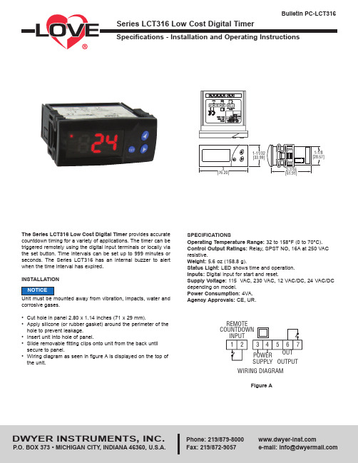
The Series LCT316 Low Cost Digital Timer provides accurate countdown timing for a variety of applications. The timer can be triggered remotely using the digital input terminals or locally via the set button. Time intervals can be set up to 999 minutes or seconds. The Series LCT316 has an internal buzzer to alert when the time interval has expired. INSTALLATION Unit must be mounted away from vibration, impacts, water and corrosive gases.SPECIFICATIONSOperating Temperature Range: 32 to 158°F (0 to 70°C).Control Output Ratings: Relay, SPST NO, 16A at 250 VAC resistive.Weight: 5.6 oz (158.8 g).Status Light: LED shows time and operation.Inputs: Digital input for start and reset.Supply Voltage: 115 VAC, 230 VAC, 12 VAC/DC, 24 VAC/DC depending on model.Power Consumption: 4VA.Agency Approvals: CE, UR.©Copyright 2014 Dwyer Instruments, Inc.Printed in U.S.A. 7/14FR# R0-443676-00 Rev.2Parameter DescriptionsUt =Time unit - Minutes (min) or Seconds (sec).Top =Maximum Time Interval - For local starts via the set key.Remote starts count down from this value.Bc =Alarm - Buzzer sounds when the countdown expires oris stopped by the user via the SET key.Man =Manual Control - When the timer countdown is notdesired, the timer can be operated to open and close the relay for indefinite periods of time. Switch the relay output off and on by means of the SET key.Programming Parameters•Press set for 8 seconds. The first parameter label is shown on the display (Ut).•Move to the desired parameter with the UP and DOWN keys.•Press SET to view the value on the display.•The value can be modified with the UP and DOWN arrows.•Press SET to store the value and exit to next parameter.•Press SET and DOWN at the same time to quit programming or wait one minute and the display will automatically exit programming mode.If the timer is activated via digital input during a previously running countdown, the timer will reset to the Top parameter and initiate a new countdown.Local OperationThe user can set and activate the timer using the front keys.•During Standby mode, press SET and “0” will be shown on the display.•Modify the time interval with the UP and DOWN keys.•Press SET to enter it and start the timer (close the relay output).•To deactivate the timer (open the relay output), hold SET down for 1 second. The time interval cannot exceed the pre-programmed “Top”parameter.BUZZERWhen the timer interval has expired, an internal buzzer will beep two times. This double beep will only occur once.LED INDICATIONSUpper LED Flashes during timer countdown.Lower LEDThis indicates the system is in Manual Control Mode.DISPLAY MESSAGESIn normal operation, the countdown time will be shown on the display.• Run =Briefly displays when the timer is initiated.• End=Briefly displays on the screen when the timer is stopped or at the end of time cycle.• Off = Standby Mode.• On or Off =Displayed during manual control. • Er =Memory Error MAINTENANCEUpon final installation of the Series LCT316 Low Cost Digital Timer, no routine maintenance is required. A periodic check of system calibration is recommended. The Series LCT316 is not field serviceable and should be returned if repair is needed (field repair should not be attempted and may void warranty). Be sure to include a brief description of the problem plus any relevant application notes. Contact customer service to receive a return goods authorization number before shipping.。
数字电子计时器
数字电子计时器吴东城(常州工学院计算机信息工程学院10计一,江苏常州213002)摘要:该数字电子计时器是用数字电路技术实现时、分、秒计时的装置,具有计时及校时功能。
该数字电子计时器的时间周期为24小时,计时器显示时、分、秒,计时器的时间对应现实生活中的时钟的一秒。
根据日常生活中的观察,数字电子计时器设计成型后供扩展的方面很多——涉及到定时自动报警、按时自动打铃、定时广播、定时启闭路灯等。
因此,与机械式时钟相比具有更高的可视性和精确性,而且无机械装置,具有更长的使用寿命,所以研究数字钟及扩大其应用,有着非常现实和实际的意义。
数字电子计时器是一种典型的数字电路,其中包括了组合逻辑电路和时序电路。
目前,数字钟的功能越来越强,并且有多种专门的大规模集成电路可供选择。
但从知识储备的角度考虑,本设计是以中小规模集成电路设计数字钟的一种方法。
数字钟包括组合逻辑电路和时序电路关键词:计时器;计数器;校时;组合逻辑电路;时序逻辑电路;译码。
0 概述0.1课题的现状:由于该课题应用较为普遍,所以实现方法很多。
基于单片机原理实现,用数字电路实现,用EDA技术实现,还可用F201448技术工艺,当然,还可以通过编程实现。
0.2本课题设计的目的、意义:数字电子计时器是一种用数字电路技术实现时、分、秒计时的装置,与机械式计时器相比具有更高的准确性和直观性,企且无机械装置,具有更长的使用寿命,因此应该得到广泛使用。
本次课程设计的目的,就是为了了解数字电子计时器的原理,从而学会制作数字电子计时器,而且通过计时器的制作机一部了解各种在制作中用到的中小规模集成电路的作用及实用方法,且由于数字电子计时器包括组合逻辑电路和时序逻辑电路,通过它可以进一步学习和掌握两种电路的原理与使用方法。
0.3课题内容、要求、达到的性能指标:(1)根据计时器的方框图和指定器件,完成计时器的主体电路设计及实验;(2)利用异步时序电路的方法,设计一个24进制的时空电路,要求当计数器运行到23时59分59秒是,秒个位计数器在接受一个秒脉冲信号后,计数器自动显示为00时00分00秒,完成进制的计时要求;(3)具有校时、分、秒;(4)在实验板上安装、调试出课题所要求的计时器;(5)画出逻辑电路图,时序图,并写出报告。
数字电子计时器课程设计
数字电子计时器课程设计一、课程目标知识目标:1. 学生能理解数字电子计时器的原理和组成,掌握基础电子元件的功能和使用方法。
2. 学生能描述数字电子计时器的工作过程,包括计时、清零和预设功能。
3. 学生能够解释数字电子计时器中数字显示的原理,理解二进制与十进制的转换。
技能目标:1. 学生能够运用所学的电子元件,设计并搭建一个简单的数字电子计时器电路。
2. 学生通过实际操作,掌握测试和调试电子计时器的方法,能够解决基本的故障问题。
3. 学生能够运用逻辑思维和问题解决技巧,对电子计时器进行改进和创新。
情感态度价值观目标:1. 学生通过课程学习,培养对电子技术的兴趣和好奇心,增强对科学探究的热情。
2. 学生在小组合作中,学会分享观点,倾听他人意见,发展团队协作精神。
3. 学生通过实际操作,体验工程的实用性,培养工程意识,认识科技对生活的影响。
课程性质:本课程为实践性强的设计与制作课程,结合电子技术基础知识,培养学生的动手能力和创新思维。
学生特点:假设学生为八年级,具有一定的物理基础和动手能力,对电子技术有初步认识,对实践活动充满兴趣。
教学要求:课程应注重理论与实践相结合,鼓励学生主动探索和动手实践,强调安全操作和精确测量。
通过课程目标的实现,使学生能够综合运用所学知识,创造性地解决实际问题。
二、教学内容1. 数字电子计时器原理:- 介绍计时器的功能与组成,参照教材第二章“数字电路基础”。
- 讲解晶体管、集成电路等基本电子元件的工作原理。
2. 数字电子计时器电路设计:- 分析计时器电路图的构成,参照教材第四章“时序逻辑电路”。
- 指导学生进行电路图的绘制,选择合适的电子元件。
3. 数字显示原理与转换:- 详述七段显示器的显示原理,参照教材第三章“数字显示技术”。
- 解释二进制与十进制的转换方法,并进行实际操作演示。
4. 电路搭建与测试:- 安排学生分组进行电路搭建,参照教材第五章“电路搭建与调试”。
- 教授测试与调试技巧,指导学生解决电路中可能出现的问题。
数字计时器安全操作及保养规程
数字计时器安全操作及保养规程数字计时器是广泛应用于各个行业的一种计时设备,具有精度高、转换速度快等优点。
由于其涉及电气知识,使用不当可能存在安全隐患。
因此,为了保证数字计时器的正常使用和安全保障,制定数字计时器安全操作及保养规程是非常必要的。
一、安全操作规程1.1 使用前检查在使用数字计时器之前,应该先进行电气安全检查。
确认数字计时器的外壳、绝缘、插头、电源电压与额定电压等是否符合要求。
并对使用环境进行检查,检查地面是否有水等导电物质,以及是否符合安装要求。
1.2 操作指南在使用数字计时器时,需要遵守以下操作指南:1.在使用前,先读取使用说明书,了解数字计时器的使用方法、操作界面、设置等内容。
2.坚持使用标准电源进行电源供电。
3.敬请遵循安全、合规等指南,不要私自更改数码计时器程序。
4.避免数字计时器受到剧烈震动、高温阳光、潮湿环境等有害因素影响。
5.在使用过程中,不要私自更改数字计时器的原始设置,如受到意外影响,应该及时更新设置至原来的指令中。
6.在输出或者输入数据的过程中,避免产生静电,使用防静电工具或者清洁干燥、通风良好的坚实表面上操作。
7.避免数字计时器光学仪表被遮挡,否则会使读出来的数据不准确。
8.在数字计时器连接其它仪表或设备时应该遵守相应的安全标准规范。
1.3 关机操作在关机时,需要注意以下几点:1.首先先关闭与其它设备的连接;2.再断电与其它外部电源的连接;3.长时间未使用、电网停电、电气故障或其他原因需要关机时,要使用断电开关切断数字计时器的电源。
1.4 禁止操作的行为在使用数字计时器时,有一些操作是禁止的,包括:1.禁止未经工厂授权的人士私自拆卸数字计时器设备;2.禁止擅自更改数字计时器的程序设置、电源适配器等。
1.5 故障排除在使用数字计时器过程中,会遇到各种各样的故障,需要及时排除,以下是常见的故障排除方法:1.当出现数字计时器无法正常连接时,首先需要检查连接的电缆、插头是否正常;2.当数字计时器显示的数字无法清晰显示时,需要先检查连接线路,查看是否有松动现象;3.当数字计时器闪烁、亮度不一、数字不准确等问题时,需要进行维修或更换相应的备件。
南京理工大学数字计时器实验报告

电子电工综合实验报告——数字计时器一.实验内容。
1. 应用CD4511BCD码译码器﹑LED双字共阴显示器﹑300Ω限流电阻设计﹑安装调试四位BCD译码显示电路实现译码显示功能。
2. 应用NE555时基电路、3KΩ、1KΩ电阻、0·047UF电容和CD4040计数分频器设计,安装,调试秒脉冲发生器电路(输出四种矩形波频率f1=1HZ f2=2HZ f3≈500Hz f4≈1000Hz)。
3. 应用CD4518BCD码计数器、门电路,设计、安装、实现00′00″---59′59″时钟加法计数器电路。
4. 应用门电路,触发器电路设计,安装,调试校分电路且实现校分时停秒功能(校分时F2=2Hz)。
设计安装任意时刻清零电路。
5. 应用门电路设计、安装、调试报时电路59′53″,59′55″,59′57″低声报时(频率f3≈500Hz),59′59″高声报时(频率f4≈1000Hz)。
整点报时电路。
H=59′53″·f3+59′55″·f3+59′57″·f3+59′59″·f46.联接试验内容1.—5.各项功能电路,实现电子计时器整点计时﹑报时、校分、清零电路功能。
二.实验要求。
设计正确、布局合理、排线整齐、功能齐全。
三.器件引脚图及功能表。
1、NE555: 功能表引脚图2、CD4040:引脚图3、CD4518:功能表引脚图4、CD4511:功能表引脚图5、74LS00:功能表引脚图6、74LS20:功能表引脚图7、74LS21:功能表引脚图8、74LS74:功能表引脚图9.LED双字共阴显示器四.电子计时电路器逻辑图;五.电子计时器电路引脚接线图.六. 各单元原理图及设计过程:1、脉冲产生电路设计方法:由NE555连接成为自激多谐振荡电路,输出为周期矩形波,后经CD4040分频得到所需频率脉冲。
逻辑图:2、计时电路设计方法:计时电路的计数器,采用二-十进制加法计数器CD4518来实现。
简述数字毫秒计的使用方法
简述数字毫秒计的使用方法
数字毫秒计是一种用于测量时间间隔的计时器,其使用方法如下:
1. 打开数字毫秒计。
通常情况下,数字毫秒计的启动按钮位于
计时器的顶部中央位置。
2. 设置初始时间。
在数字毫秒计开始计时之前,您需要先将其
归零,然后根据需要设置初始时间。
3. 开始计时。
按下数字毫秒计的启动按钮,它将开始计时。
如
果需要记录多个时间,您可以按下记录按钮来保存计时器的当前读数。
4. 停止计时。
当您需要停止计时器时,再次按下启动按钮,计
时器将停止计时。
5. 重置数字毫秒计。
在完成计时任务后,您可以按下重置按钮,将数字毫秒计的读数归零,准备下一次使用。
总体来说,数字毫秒计非常简单易用,并在许多领域都有广泛的
应用,包括计算机编程、体育和科学实验等。
电子电工实验报告——数字计时器
南京理工大学电子电工综合实验(Ⅱ)--数字计时器实验报告专业:通信工程班级:9141042202姓名:许雪婷学号:9141133702082016年09月目录一、实验目的、要求及内容;二、器件引脚图及功能表;三、各单元电路的原理、设计方法及逻辑图;四、数字计时器电路引脚接线图;一、 实验目的、要求及内容1.实验目的① 掌握常见集成电路实现单元电路的设计过程。
② 了解各单元再次组合新单元的方法。
2.实验要求实现00’00”—59’59”的可整点报时的数字计时器。
3.实验内容① 设计实现信号源的单元电路。
(KHz F Hz F Hz F Hz F 14,5003,22,11≈≈≈≈) ② 设计实现00’00”—59’59”计时器单元电路。
③ 设计实现快速校分单元电路。
含防抖动电路(开关k1,频率F2,校分时秒计时器停止)。
④ 加入任意时刻复位单元电路(开关K2)。
⑤ 设计实现整点报时单元电路(产生59’53”,59’55”,59’57”,三低音频率F3,59’59”一高音频率F4)。
二、器件引脚图及功能表元件清单:集成电路:NE555 一片,CD4040 一片,CD4518 二片,CD4511 四片,74LS00 三片,74LS20 一片,74LS21 三片,74LS74 一片。
电阻:1KΩ一只,3KΩ一只,150Ω四只。
电容:0.047uF 一只。
LED共阴双字屏二块。
1、NE555图1-1 NE555引脚图图1-2 NE555逻辑功能表2、CD4040图2-1 CD4040引脚图图2-2 CD4040功能表3、CD4518图3-1 CD4518引脚图图3-2 CD4518功能表4、CD4511图2-1 CD4511引脚图图2-2 CD4511逻辑功能表5、74LS0074LS00是一种集成了4个与非门的集成电路。
图5-1 74LS00引脚图图5-2 与非门逻辑表6、74LS2074LS20同样是一种与非门集成电路,与74LS00不同的是它的每个与非门有4个输入端。
WMF数字快速计时器说明书
数字定时器Stellen Sie durch Drücken des MIN und SEC Felds die gewünschte Zeit ein. Drücken Sie die START/STOP Taste um den Kurzzeitmesser zu starten.Durch Drücken der START/STOP Taste können Sie die Zeit unterbrechen und wieder starten.Durch gleichzeitiges Drücken der MIN und SEC setzen Sie die Zeit auf 00:00 zurück.Wenn Sie bei 00:00 die START/STOP Taste drücken, läuft die Zeit vor-wärts und Sie können den Kurzzeitmesser als Stoppuhr nutzen.Bei Nichtgebrauch erlischt das Display nach kurzer Zeit.Bitte beachten Sie Den Kurzzeitmesser keinen extremen Temperaturschwankungen ausset-zen. Verschmutzungen mit einem feuchten Tuch abwischen.CE-Konformität Dieses Gerät ist funkentstört entsprechend der geltenden EG-Richtlinie 004/108/EG.Hinweis: Unter extremen elektromagnetischen Einflüssen, z.B. bei Betreiben eines Funkgerätes in unmittelbarer Nähe des Kurzzeitmessers, kann eine Beeinflussung des Anzeigewertes verursacht werden. Nach Digitaler KurzzeitmesserTechnische DatenMaximale Zeiteinstellung: 99 min und 59 secEin-/Abschaltknopf auf der RückseiteZwei 1,5 V Batterien AAA (im Lieferumfang enthalten)Bitte lesen Sie die Bedienungshinweise vollständig durch, bevor Sie den Kurzzeitmesser zum ersten Mal benutzen.Bewahren Sie die Anleitung zum Nachlesen bitte sorgfältig auf.Falls Sie den Kurzzeitmesser an einen anderen Benutzer weitergeben, händigen Sie ihm die Anleitung zusammen mit dem Produkt aus.Vor dem ersten GebrauchÖffnen Sie den Batteriefachdeckel auf der Rückseite und entnehmen Sie die Batterien. Entfernen Sie die Schutzfolie und legen Sie die Batterien entsprechend der Polaritätszeichen wieder ein. Schließen Sie den Deckel. Hinweise zur BedienungStellen Sie den kleinen Schieber auf der Rückseite auf ON.Der Touch Screen reagiert auf Berührung.stelle für das Recycling von elektrischen und elektroni- schen Geräten abgegeben werden muss. Weitere Informa- tionen erhalten Sie über Ihre Gemeinde, die kommunalen Entsorgungs-betriebe oder das Geschäft, in dem Sie das Produkt gekauft haben.Sicherheitshinweise für Lithiumbatterien (CR2032/CR2430)• Bei Lithiumbatterien handelt es sich um Lithium-Mangan-Zellen. Wenn Sie den Kurzzeitmesser über einen längeren Zeitraum nicht benutzen, sollten Sie die Batterien aus dem Gerät nehmen.• Bitte nie die Lithiumbatterien öffnen, ins Feuer werfen oder Stößen aussetzen, da möglicherweise giftige Dämpfe austreten oder Explosi-onsgefahr besteht.• Fassen Sie ausgelaufene Zellen nie mit bloßen Händen an.• Bei Kontaminierung der Augen oder Hände unbedingt mit viel Wasser spülen, bei Reizungen der Haut oder Augen sollten Sie einen Arzt aufsuchen.• Entsorgen Sie nur vollständig entladene oder verpolungssicher ver-packte Zellen, entsprechend den örtlichen Entsorgungsvorschriften.• Setzen Sie die Zellen nicht direkter Sonneneinstrahlung und großer Hitze aus, da ansonsten die Gefahr von Überhitzung besteht. Halten Sie eine Lagertemperatur von < 40°C ein.Ende des Störeinflusses ist das Produkt wieder bestimmungsgemäß benutzbar, ggfls. ist ein Wiedereinschalten erforderlich.Gesetzliche Hinweispflicht zur EntsorgungAltbatterienBatterien gehören nicht in den Hausmüll. Als Verbrauchersind Sie gesetzlich dazu verpflichtet, gebrauchte Batterienzurückzugeben. Sie können Ihre alten Batterien bei den öf-fentlichen Sammelstellen in Ihrer Gemeinde oder überall dortabgeben, wo Batterien der betreffenden Art verkauft werden.Hinweis:Diese Zeichen finden Sie auf Batterien:Li = Batterie enthält LithiumAl = Batterie enthält AlkaliMn = Batterie enthält ManganCR (Li); AA (Al, Mn); AAA (Al, Mn)Elektrische/Elektronische GeräteDas Symbol auf dem Produkt oder seiner Verpackung weistdarauf hin, dass dieses Produkt nicht als normaler Haus-haltsabfall zu behandeln ist, sondern an einer Annahme-The touch screen reacts to contact. Set the desired time by pressing the MIN and SEC field. Press the START/STOP button to start the cooking timer.By pressing the START/STOP button you can stop and restart the timing process.Pressing MIN and SEC simultaneously will reset the time to 00:00.If you press the START/STOP button when the display reads 00:00, the time starts to run and you can use the cooking timer as a stopwatch.When not in use the display goes out after a short period of time.Please note Do not expose the cooking timer to any extreme fluctuations in temperature. Wipe off marks with a damp cloth.CE conformity This device is shielded from interference and voltage peaks in accord-ance with the applicable EC Directive 004/108/EC. Note: under extreme electromagnetic influences, for instance when a radio is operated in the immediate vicinity of the cooking timer, the readout may be affected. The product can be used again normally once the disruptive influence is no longer present, although it may be necessary to switch it back on.Digital cooking timerTechnical dataMaximum time setting: 99 mins and 59 secsOn/off button on the backTwo 1.5 V AAA batteries (included in the delivery)Please read the instructions for use thoroughly before using the cook-ing timer for the first time.Please keep the instructions in a safe place for subsequent reference. If you pass on the cooking timer to another user, give him the instruc-tions along with the product.Before using for the first timeOpen the battery compartment on the back and remove the batteries. Remove the protective film and replace the batteries, observing the polarity signs. Close the lid.How to use the cooking timerPosition the small slider on the back to ON.Safety instructions for lithium batteries (CR2032/CR2430)• Lithium batteries contain lithium-manganese cells. The batteries should be removed from the device if you will not be using the cooking timer for a long period of time.• Never open the lithium batteries, discard them into a fire or subject them to any impact as toxic vapours may escape as a result and there is also the risk of the batteries exploding.• Never touch discharged batteries with your bare hands.• In the event of contamination of the eyes or skin, immediately rinse with plenty of water, you should seek medical advice if the eyes or skin become irritated.• Only dispose of completely discharged batteries or batteries pa-ckaged so as to protect against reverse polarity, and in accordance with the local disposal regulations.• Do not expose the batteries to direct sunlight or extreme heat, as otherwise there is the danger of overheating.• Ensure the storage temperature is < 40°C.Obligatory legal notification regarding disposalUsed batteriesBatteries should not be placed with household refuse. As aconsumer, you are legally obliged to return used batteries.You can leave used batteries at the public collection pointsin your community or hand them in wherever batteries ofthe type in question are sold.Note:You will find these letters on batteries:Li = battery contains lithiumAl = battery contains an alkaliMn = battery contains manganeseCR (Li); AA (Al, Mn); AAA (Al, Mn)Electric/electronic devicesThe symbol on the product or its packaging indicates that this product must not be treated as normal household waste, but must be taken to a collection point for the recycling of electric and electronic devices. Further information can be obtained from your community, the munici-pal disposal operators or the shop where you bought the product.L‘écran tactile réagit au toucher. Fixez le temps souhaité en appuyant sur les champs MIN et SEC. Appuyez sur la touche START/STOP pour démarrer le minuteur.En appuyant sur la touche START/STOP, vous pouvez interrompre le temps et redémarrer.En appuyant simultanément sur MIN et SEC, vous remettez le compteur à zéro.Si vous appuyez sur la touche START/STOP à 00:00, le temps commence à s‘écouler et le minuteur peut vous servir de chronomètre.En cas de non utilisation, l‘écran s‘éteint au bout d‘un court instant.Attention N‘exposez pas le minuteur à des écarts de températures extrêmes.Essuyez les saletés à l‘aide d‘un chiffon humide.Conformité CE Cet appareil est antiparasité conformément à la directive 004/108/CE en vigueur.Consigne : L‘influence électromagnétique extrême, par ex. une radio en service à proximité immédiate du minuteur, peut affecter la valeur affichée. Une fois ces perturbations terminées, le produit est à nouveau Minuteur numériqueCaractéristiques techniquesRéglage du temps maximum : 99 min et 59 secBouton marche/arrêt sur la face arrièreDeux piles AAA de 1,5 V (comprises dans la livraison)Veuillez lire attentivement les conseils d‘utilisation avant d‘utiliser le minuteur pour la première fois.Conservez précieusement le mode d‘emploi après l‘avoir lu.Si vous confiez le minuteur à un autre utilisateur, remettez-lui aussi le mode d‘emploi.Avant la première utilisationOuvrez le couvercle du compartiment à piles sur la face arrière et retirez les piles. Retirez la pellicule de protection et reposez la pile en respectant les signes de polarité. Fermez le couvercle.Conseils d‘utilisationRéglez le petit curseur sur ON sur la face arrière.électroniques. Vous obtiendrez des informations plus détaillées auprès de votre commune, des déchetteries communales ou du magasin où vous avez acheté le produit.Consignes de sécurité pour les piles en lithium (CR2032/CR2430)• Pour les piles en lithium, il s‘agit de la catégorie lithium-manganèse. Si vous n‘utilisez pas le minuteur pendant une longue période, il vaut mieux enlever les piles de l‘appareil.• N‘ouvrez jamais les piles en lithium, ne les jetez pas au feu et ne les exposez pas à des chocs car vous multipliez les risques d‘explosion ou que des vapeurs toxiques se dégagent.• N‘attrapez pas les piles usées à mains nues.• Rincez immédiatement à grande eau en cas de contamination des yeux ou des mains et en cas d‘irritation de la peau ou des yeux, nous vous invitons à consulter un médecin.• Éliminez uniquement des piles emballées selon la bonne polarité et complètement déchargées conformément aux prescriptions d‘élimination.• N‘exposez pas les piles aux rayons directs du soleil ou à une forte chaleur car elles risquent de se surchauffer.• Maintenez une température de stockage < 40 °C.opérationnel et un redémarrage serait judicieux, le cas échéant.Obligation légale d‘éliminationPiles usagéesLes piles ne se jettent pas dans les ordures ménagères. Entant que consommateur, vous êtes légalement tenus derestituer les piles usagées. Vous pouvez déposer vos pilesusagées dans les centres de collecte publics de votre com-mune ou auprès de n‘importe quel point de vente de pilesdu même type.Consigne :Vous trouverez ces caractères sur les batteries :Li = la pile contient du lithiumAl = la pile contient de l‘alcaliMn = la pile contient du manganèseCR (Li) ; AA (Al, Mn) ; AAA (Al, Mn)Appareils électriques/électroniquesLe symbole sur le produit ou son emballage indique que le produit ne doit pas être traité comme les ordures ménagères et doit être remis à un centre de collecte pour le recyclage des appareils électriques etLa pantalla táctil reacciona al tocarla. Ajuste el tiempo deseado pulsando los campos de MIN y SEC. Pulse la tecla START/STOP para activar el avisador de cocina.Al pulsar la tecla START/STOP, podrá parar y volver a iniciar el tiempo.Si pulsa al mismo tiempo MIN y SEC, el tiempo volverá a ponerse a 00:00.Si pulsa la tecla START/STOP con el tiempo a 00:00, este comenzará a contar hacia delante y podrá utilizar el avisador como temporizador.Si tras un breve periodo de tiempo la pantalla no se utiliza, se apaga.Atención No exponga al avisador de cocina a cambios extremos de temperatura.Limpie la suciedad con un paño húmedo.Conformidad CE Este aparato no interfiere en las ondas electromagnéticas, de conformi-dad con la normativa vigente CE 004/108/CE. Advertencia: bajo cargas extremas electromagnéticas, como por ejemplo el funcionamiento de una radio al lado del avisador de cocina, podría producirse una interferencia en el valor del indicador. Una vez eliminada la interferencia, ya puede volver a utilizar el aparato confor-Avisador de cocina digitalDatos técnicosAjuste temporal máximo: 99 min y 59 sBotón de conexión/desconexión en la parte traseraDos pilas de 1,5 V AAA (incluidas en el envío)Léase las indicaciones de manejo al completo antes de utilizar elavisador de cocina por primera vez. Guárdese las instrucciones de forma segura para una posterior consulta y lectura.Si va a pasar el avisador de cocina a otro usuario, no olvide entregarle también las instrucciones de uso junto con el producto.Antes del primer usoAbra la tapa del compartimento de pilas colocada en la parte trasera y sá- quelas. Elimine el adhesivo protector y vuelva a introducir las pilas tenien-do en cuenta los correspondientes símbolos de polaridad. Cierre la tapa. Indicaciones de usoColoque el pequeño cursor de la parte trasera en posición ON.municipal de basuras y eliminación o en el comercio donde adquirió el producto.Advertencias de seguridad para pilas de litio (CR2032/CR2430)• Las pilas de litio son células de litio y manganeso. Si no va a utilizar el avisador de cocina durante un largo tiempo, es recomendable que saque las pilas del aparato.• No abra nunca las pilas de litio, ni las arroje al fuego o las agujere, ya que es posible que salga gas tóxico e incluso exista peligro de explosión.• No toque nunca las pilas con líquido derramado con las manos desnudas.• En caso de contacto con ojos o manos, lávese inmediatamente con agua abundante y si aparece irritación en la piel o los ojos consulte al médico.• Deposite en la basura solo las pilas completamente descargadas o las envueltas en seguridad de polarización según las normativas de eliminación locales vigentes.• No exponga nunca las pilas a la luz solar directa o a una fuente de calor elevada ya que existe peligro de sobrecalentamiento.• Almacenar a una temperatura inferior a 40 ºC.me a su uso; a veces es necesario reiniciarlo.Obligación legal de advertencia para la eliminaciónPilas usadasLas pilas no pueden depositarse en la basura doméstica.Como consumidor, usted está obligado por la ley a devolverlas pilas usadas. Puede depositar sus pilas usadas en puntosoficiales de recogida de su municipio o dejarlas en cualquiercomercio que venda pilas de esa clase.Nota:En las pilas encontrará estos símbolos:Li = la pila contiene litioAl = la pila contiene metal alcalinoMn = la pila contiene manganesoCR (Li); AA (Al, Mn); AAA (Al, Mn)Aparatos eléctricos y electrónicosEl símbolo colocado en el producto o en su envase indica que no debe tratarse como si fuera un residuo normal doméstico, sino que debe lle-varse a un punto de recogida para el reciclaje de aparatos electrónicos yeléctricos. Podrá obtener más información en su ayuntamiento, oficinaIl touchscreen reagisce al contatto. Impostare il tempo desiderato premendo su MIN e SEC. Premere il tasto START/STOP per azionare il timer da cucina.Premendo il tasto START/STOP è altresì possibile interrompere e ripren-dere il conteggio.Premendo contemporaneamente i tasti MIN e SEC, il timer da cucina viene resettato su 00:00. Impostato su 00:00, il timer da cucina può es-sere utilizzato come cronometro, premendo i tasti START/STOP. In caso di non utilizzo, il display si spegne automaticamente dopo alcuni istanti.AttenzioneNon esporre il timer a oscillazioni estreme di temperatura.Rimuovere lo sporco con un panno umido.Conformità CEQuesto dispositivo è radioschermato in conformità alla direttiva CE vigente: 004/108/CE.Nota: a causa di influssi elettromagnetici estremi, per esempio attivan-do un apparecchio radio nelle immediate vicinanze del timer da cucina, è possibile che il valore visualizzato subisca delle alterazioni. Terminata l’interferenza, il prodotto è di nuovo utilizzabile secondo gli scopi edTimer digitale da cucinaDati tecniciTempo massimo impostabile: 99 min e 59 sec.Pulsante di attivazione/disattivazione del timer, posizionato nella parte posteriore. Due batterie di tipo AAA, da 1,5 V (incluse nella fornitura).Leggere attentamente le istruzioni per la manutenzione prima di iniziare a utilizzare il timer da cucina. Conservare scrupolosamente il presente manuale per consultazioni future.Se il timer da cucina viene ceduto a un altro utente, quest’ultimo deve entrare in possesso anche del relativo manuale.Prima dell’uso inizialeAprire il coperchio del vano batterie sul lato posteriore, quindi prendere le batterie. Rimuovere la pellicola di protezione e riposizionare le batte-rie rispettando la polarità. Chiudere il coperchio. Consigli per l‘usoPosizionare il piccolo pulsante posteriore su ON.2120più dettagliate è possibile rivolgersi all’ufficio comunale, al servizio locale di smaltimento dei rifiuti oppure al nego-zio in cui è stato acquistato il prodotto.Indicazioni di sicurezza per le batterie al litio (CR2032/CR2430)• Per “batteria al litio” si intende una batteria a bottone litio-manga-nese. Si consiglia di rimuovere le batterie dell’apparecchio in caso di non utilizzo prolungato del timer da cucina.• Non aprire in nessun caso le batterie al litio, non gettarle nel fuoco e non esporle a sollecitazioni di alcun genere poiché si potrebbero sprigionare vapori velenosi o verificare rischi di esplosione.• Non afferrare mai a mani nude le batterie con perdite.• In caso di contatto con gli occhi o le mani, risciacquare con molta acqua. In presenza di irritazioni cutanee o oculari si consiglia di contattare un medico.• Smaltire le batterie a bottone completamente esaurite o imballate per impedire l’inversione delle polarità, in conformità alle disposizio-ni locali in materia di smaltimento.• Non esporre le batterie a bottone alla luce diretta del sole e a tempe-rature molto elevate perché altrimenti si rischia il surriscaldamento.• Rispettare la temperatura di stoccaggio inferiore a 40 °C.eventualmente è necessaria una sua riaccensione.Obbligo di avviso secondo la legge sulle batterie Batterie esauriteLe batterie esaurite non devono essere considerate rifiuti domestici. Il consumatore è tenuto per legge alla restituzio-ne delle batterie scariche. È possibile restituire gratuita-mente le batterie usate al proprio rivenditore o consegnarle ai centri di raccolta comunali.Nota:sulle batterie sono riportate le seguenti sigle:Li = la batteria contiene litio Al = la batteria contiene alcaliMn = la batteria contiene manganese CR (Li); AA (Al, Mn); AAA (Al, Mn)Dispositivi elettrici/elettroniciQuesto simbolo sul prodotto o sulla confezione indica che il prodotto non deve essere considerato come un normale rifiuto domestico, ma deve invece essere consegnato a un punto di raccolta appropriato peril riciclo di apparecchi elettrici ed elettronici. Per ricevere informazioni2322同时点击 MIN 和 SEC 按键将时间重置到 00:00。
数字计时器的原理及应用
数字计时器的原理及应用一、引言数字计时器是一种常见的电子设备,它可用于测量时间、计数和显示时间等功能。
本文将介绍数字计时器的原理、工作方式和应用领域。
二、数字计时器的原理数字计时器的原理基于电子时钟和计数器的技术。
它由微处理器、晶振、计数器芯片和显示屏等部件组成。
数字计时器的原理如下: 1. 微处理器:微处理器是数字计时器的核心部件,负责控制整个计时器的工作。
它接收外部信号并进行处理,然后将结果发送到显示屏上。
2. 晶振:晶振是数字计时器的时钟源,它提供稳定的时钟信号给微处理器,确保计时器的准确性。
3. 计数器芯片:计数器芯片用于记录和计时输入的信号。
它包含一个或多个计数器,可以精确地计算输入信号的数量和时间间隔。
4. 显示屏:显示屏用于将计时器的结果显示出来。
通常采用LED或LCD技术,能够清晰地显示数字和其他信息。
三、数字计时器的工作方式数字计时器的工作流程如下: 1. 初始化:计时器通过微处理器初始化,并设置初始数值。
2. 接收输入信号:计时器通过输入端口接收外部输入信号。
这些信号可以来自按钮、传感器或其他外部设备。
3. 计时和计数:计时器根据接收到的信号进行计时和计数操作。
它会记录信号的数量和时间间隔,然后将结果存储在计数器芯片中。
4. 显示结果:计时器通过微处理器将计时和计数结果发送给显示屏,以便用户查看。
四、数字计时器的应用领域数字计时器在各个领域都有广泛的应用,包括但不限于以下几个方面:1. 运动计时数字计时器可以应用于运动领域,如田径比赛、游泳比赛和赛车比赛等。
它能够精确记录参赛者的计时,并提供实时的计时结果,方便裁判判断比赛成绩。
2. 实验测量在科学实验和工程测量中,数字计时器可以用于测量时间间隔、周期和频率等参数。
它能够高精度地记录信号的变化,并提供准确的测量结果。
3. 工业生产数字计时器在工业生产中起到重要的作用。
它可以帮助工人记录和计时生产过程中的关键步骤和时间,提高生产效率和质量。
- 1、下载文档前请自行甄别文档内容的完整性,平台不提供额外的编辑、内容补充、找答案等附加服务。
- 2、"仅部分预览"的文档,不可在线预览部分如存在完整性等问题,可反馈申请退款(可完整预览的文档不适用该条件!)。
- 3、如文档侵犯您的权益,请联系客服反馈,我们会尽快为您处理(人工客服工作时间:9:00-18:30)。
电工电子综合实验报告—数字计时器院系:电光学院专业:通信工程班级:07042201学号:0704220100姓名:* * *指导教师:李元浩时间:2009.09.17—2009.09.20目录1.设计电路功能要求(1)2.设计电路原理图(1)3.电路逻辑原理图及工作原理(2)4.各单元电路原理及逻辑设计4.1脉冲发生电路(2-3)4.2计时电路(3-4)4.3显示电路(4)4.4清零电路(5)4.5校分电路(5)4.6报时电路(6)5.电路安装与调试说明(6-7) 6.对电路的改进意见(7)7.收获体会及建议(7)8.设计参考资料(7)9.附录(8-10)1.设计电路功能要求本实验要求设计一个0分00秒-9分59秒的多功能数字计时器。
数字计时器是由脉冲发生电路,计时电路,译码显示电路,和控制电路等几部分组成。
其中控制电路由清零电路,校分电路,和报时电路组成。
该数字计时器可以在控制电路的作用下具有开机清零、手动清零、快速校分和整点报时功能。
①.设计一个脉冲发生电路,为计时器提供秒脉冲,为报时电路提供驱动蜂鸣器发声的脉冲信号;②.设计计时和显示电路,将分及秒的个位、十位分别在七段显示器上显示出来,从0分0秒开始,计到9分59秒,然后重新计数。
将分及秒的个位、十位分别在七段显示器上显示出来,七段显示器循环显示数字000~959;③.设计清零电路,实现手动及开机清零;④.设计校分电路,在校分开关控制下实现分校正;⑤.设计报时电路,使数字计时器实现在9分53秒、9分55秒、9分57秒低音(1KHz)报时,以及在9分59秒高音(2KHz)报时;2.设计电路原理图图2-1 电路原理图3.电路逻辑原理图及工作原理数字计时器的原理方框图如图3-1所示,该电路系统由脉冲发生电路、计时和显示电路、清零电路、校分电路和报时电路和其它附加电路等几部分组成的。
脉冲发生电路由振荡器和分频器组成,振荡器产生稳定的高频脉冲信号,作为数字钟的时间基准,再经分频器输出标准的秒脉冲,同时也可得到其他不同频率的脉冲。
电路要实现0分00秒至9分59秒的计时和显示功能,所以由三个计时器分别计时,分位(模10)、秒十位(模6)、秒个位(模10),然后再通过译码器,由LED数字显示管显示出来。
清零电路实现开机清零和任意时刻手动清零,通过逻辑门与计时器连接,从而实现清零。
校分电路实现快速校分,只要将分计数器的频率调快等操作即可实现。
报时电路是根据计时电路的输出状态产生一个脉冲信号,然后去触发蜂鸣器实现报时。
图3-1 数字计时器原理方框图4.各单元电路原理及逻辑设计4.1脉冲发生电路脉冲发生电路是计时器的核心部分,它提供计时电路的时钟并为报时电路提供驱动信号。
脉冲发生电路是由振荡器和分频器构成,其原理图如图4-1。
一般来说,振荡器的振荡频率越高,及时精度越高。
本实验采用的石英晶体多谐振荡器的频率为32768Hz。
分频器CD4060内部有14级二分频器,有两个反相器,最大可实现分频,所以可输出的最低频率为2Hz;为了得到1Hz的脉冲,需要在振荡器后再加一级二分频器,只要将D触发器的端与D端连接在一起就可以用D触发器实现二分频,所以在CD4060的Q14端接一个D触发器,即可以输出频率为1Hz的脉冲信号。
同时CD4060也可提供报时电路所需要的频率为1KHz和2KHz的脉冲信号。
图4-1脉冲发生电路4.2 计时电路计时电路由分计数器、秒十位计数器和秒个位计数器构成。
一片CD4518含有两个十进制计数器,因此可以用一片CD4518组成秒计数器的个位和分计数器的十位计数。
用一片74LS161构成一个模六计数器就可以实现秒十位的计数。
秒个位:连接电路时,秒信号发生器产生的秒脉冲信号送入秒个位计数器CD4518的CP端,上升沿触发,秒个位单元中的输出Q4通过非门接入74LS161的时钟端,当输入第十个脉冲时,Q4输出跃变,产生进位脉冲,完成个位与十位的进位。
秒十位:秒十位记数器应实现模六功能,可以采用反馈置位法,Q1和Q3通过一与非门接入置数端,74LS161的四个数据输入端接地,这样当计数器的状态0101时,时钟到来的时候又重新置数为0000。
分位:分计数器的电路与秒个位计数器相似,用CD4518实现十进制计数功能,把74LS161的Q3接到分计时电路CD4518的引脚CP端,上升沿触发,作为进位信号。
电路原理图如图4-2:图4-2 计时电路图4.3 译码显示电路计时器的输出(用二进制代码表示的数),经译码器驱动数码显示器,就可以直接显示出数字。
本实验采用三片CD4511显示译码器和三个七段共阴LED显示管,电路从0分00秒计到9分59秒,译码显示电路用三片四线七线译码器CD4511进行译码,然后用共阴极七段LED数码管进行显示。
CD4511的输入端应与相应计数器的输出相连,而它的输出端应与数码管的管脚对应相连,而CD4511每个输出端与数码管对应管脚相连时还应连接一个300欧姆的电阻,以起保护作用。
为了使CD4511工作在译码状态,必须LT=1,BI=1,LE=0。
其电路原理图如图4-3:图4-3 译码显示电路图4.4 清零电路清零电路要实现两项功能:开机清零和任意时刻手动清零。
开机清零是指在电路刚刚上电时可以使所有的计数器自动复位,即从零开始工作。
手动清零是指在电路正常工作时,按动清零开关,使计数器全部回零。
开机清零是通过电容两端电压的非调变特性实现的。
电路刚接通电源时,节点处的电位为1。
该电位经过一个反相器接入秒十位计数器的Cr端,经过两个反相器接入分计数器和秒个位计数器的Cr端,则这三个计数器的清零端均接入有效电平,实现清零。
此后,只要电源始终保持接通,电路持续计数,开机清零电路就失效了。
断开清零开关时,节点1处电位为5V,此时送入各计数器清零端的信号均为无效信号,无法实现清零。
而闭合清零开关时,因为电容要充电,所以节点1处电位为1,送入各计数器清零端的信号均有效,电路实现清零。
其电路原理图如图4-4:图4-4 清零电路图4.5 校分电路校分电路是由开关和逻辑门电路实现的。
当校分电路开关打开时,计数器正常计数;当开关闭合时,秒个位和秒十位正常计数,分位进行快速校分,即分计数器可以不受秒计数器的进位信号的控制。
当开关合上时,2Hz的信号通过与非门,秒十位计数器的次高位进位脉冲被截止,与非门输出高电平,这时2Hz的信号可以再通过一次与非门,把2Hz的脉冲送入分计数器时钟脉冲端,实现快速校分。
其电路原理图如图4-5:图4-5 校分电路图4.6 报时电路报时电路由逻辑门电路组成的。
需要在某一时刻报时,就将该时刻输出为“1”的信号作为触发信号,选通报时脉冲信号,进行报时。
按照设计要求,数字计时器应在9分53秒、9分55秒、9分57秒发低音(频率1KHz),9分59秒发高音(频率2KHz)。
它们持续的时间均为一秒,如表一所示:表4-1 秒个位计数器的状态CP(秒)Q3 Q2 Q1 Q0 功能50 0 0 0 051 0 0 0 152 0 0 1 053 0 0 1 1 鸣低音54 0 1 0 0 停55 0 1 0 1 鸣低音56 0 1 1 0 停57 0 1 1 1 鸣低音58 1 0 0 0 停59 1 0 0 1 鸣高音00 0 0 0 0 停当分的状态为Q3Q2Q1Q0=1001,秒十位的状态为Q3Q2Q1Q0=0101以及秒个位的Q0=1时,用秒个位的Q3、Q2、Q1的状态来控制1KHz或2KHz得信号输入:当Q2+Q1=1时,输入1KHz的信号;当Q3=1时,输入2KHz的信号。
其电路原理图如图4-6:图4-6 报时电路图所用集成器件引脚功能及真值表见附录。
5.电路安装与调试说明根据计时器整机框图和前面所学的模块知识,将计时器的各个单元电路组合起来,构成图2-1所示的计时器原理电路图。
在完成整机电路连接之前,应先对各单元电路进行逐一安装和调试,然后再进行整机的连接与调试。
由于这次实验较为复杂,而且准备时间不够,实验过程中出现了很多问题。
1.混淆了各类元器件引脚悬空的含义。
解决方法:实验前,做好充分的预习,画出元器件的引脚图和功能表。
2.清零电路不能实现清零功能。
解决方法:经过检查,发现是所用电阻阻值太大,更换电阻后,电路正常工作。
3.秒脉冲信号发生器不能产生脉冲。
解决方法:经过检查,发现电源没有接通,重新连接之后,电路产生了所需脉冲。
还有最重要的一点是连接电路时最好分块连接,逐步调试,以便及时发现问题。
6.对电路的改进意见①在开关处加一个RS锁存器可以消颤,使输入更稳定。
②给电路增加一个定时器,该计时器可在计时范围内任意设定工作时间长短、能自动及时并具有定时警示功能的装置。
7.收获体会及建议这次实验相对以前做的数电实验来说复杂了很多,由于时间紧迫,在图书馆查阅了一些资料后,就设计出了大致的实验原理图。
这次实验由于电路复杂,用到的元器件多,在连接的时候很容易出错,所以在连接电路的时候,分块连接,脉冲发生电路、计时和显示电路、清零电路、校分电路和报时电路,这样每连好一小块后,马上进行调试,纠正电路中的错误,直到实现该模块的功能才进行下一小块的连接。
连线的时候,尽量横平竖直,不要出现线线交叉,更不要使导线跨过芯片连接,否则,当芯片损坏时不易更换。
而且,所有芯片应该先把电源和接地端连好。
在实验中我们应该学会用万用表来检测元器件的好坏,这样更容易帮助我们发现问题所在。
总的来说,这次实验完成地比较顺利,虽然过程很繁琐,由于为了不使导线交叉,所以需要剪出大量的短导线来连接,这使得人头昏眼花的,但是相对实验成果来说,这是非常值得的,不管怎么说,付出的努力都有了回报。
通过这一周的学习,我感觉有很大的收获:首先,通过学习使自己对课本上的知识可以应用于实际,使的理论与实际相结合,加深自己对课本知识的更好理解,同时实习也段练了我个人的动手能力,对我们学生来说,理论与实际同样重要,这是我们以后在工作中说明自己能力的一个重要标准;能够充分利用图书馆去查阅资料,增加了许多课本以外的知识。
经过这次实验,我对数字电路有了更加深刻的理解,了解了数字电路在实践中的应用。
最后,感谢老师在实验中对我的帮助。
8.设计参考资料①《数字逻辑电路与系统设计》蒋立平著南京理工大学 2001②《实验电子技术》李振声主编国防工业出版社 2001③《电子技术实验指导书》马鑫金编南京理工大学 2006④《电子技术实验教程》赵立明主编机械工业出版社 2008⑤《电子技术实验及课程设计》李贵安主编东南大学出版社 20089.附录①.工具及器件清单②各元件的引脚图及功能表元件引脚图。