锁相式数字频率合成器设计
MC145157锁相环频率合成器

PLL Frequency Synthesizer FamilyCMOSThe devices described in this document are typically used as low–power,phase–locked loop frequency synthesizers. When combined with an external low–pass filter and voltage–controlled oscillator, these devices can provide all the remaining functions for a PLL frequency synthesizer operating up to the device’s frequency limit. For higher VCO frequency operation, a down mixer or a prescaler can be used between the VCO and the synthesizer IC.These frequency synthesizer chips can be found in the following and other applications:CATV TV Tuning AM/FM Radios Scanning Receivers Two–Way Radios Amateur RadioCONTENTSPageDEVICE DETAIL SHEETSMC145151–2 Parallel–Input, Single–Modulus 2. . . . . . . . . . . . . . . . . . . . . . . . . . . . . . . . . . . . . . . . . . . . . . . . . . . . . . . . . . . . . . . . . . MC145152–2 Parallel–Input, Dual–Modulus 5. . . . . . . . . . . . . . . . . . . . . . . . . . . . . . . . . . . . . . . . . . . . . . . . . . . . . . . . . . . . . . . . . . . MC145155–2 Serial–Input, Single–Modulus 9. . . . . . . . . . . . . . . . . . . . . . . . . . . . . . . . . . . . . . . . . . . . . . . . . . . . . . . . . . . . . . . . . . . MC145156–2 Serial–Input, Dual–Modulus 13. . . . . . . . . . . . . . . . . . . . . . . . . . . . . . . . . . . . . . . . . . . . . . . . . . . . . . . . . . . . . . . . . . . . MC145157–2 Serial–Input, Single–Modulus 17. . . . . . . . . . . . . . . . . . . . . . . . . . . . . . . . . . . . . . . . . . . . . . . . . . . . . . . . . . . . . . . . . . MC145158–2 Serial–Input, Dual–Modulus 20. . . . . . . . . . . . . . . . . . . . . . . . . . . . . . . . . . . . . . . . . . . . . . . . . . . . . . . . . . . . . . . . . . . . FAMILY CHARACTERISTICSMaximum Ratings 23. . . . . . . . . . . . . . . . . . . . . . . . . . . . . . . . . . . . . . . . . . . . . . . . . . . . . . . . . . . . . . . . . . . . . . . . . . . . . . . . . . . . . . . . DC Electrical Characteristics 23. . . . . . . . . . . . . . . . . . . . . . . . . . . . . . . . . . . . . . . . . . . . . . . . . . . . . . . . . . . . . . . . . . . . . . . . . . . . . . . AC Electrical Characteristics 25. . . . . . . . . . . . . . . . . . . . . . . . . . . . . . . . . . . . . . . . . . . . . . . . . . . . . . . . . . . . . . . . . . . . . . . . . . . . . . . Timing Requirements 26. . . . . . . . . . . . . . . . . . . . . . . . . . . . . . . . . . . . . . . . . . . . . . . . . . . . . . . . . . . . . . . . . . . . . . . . . . . . . . . . . . . . . . Frequency Characteristics 27. . . . . . . . . . . . . . . . . . . . . . . . . . . . . . . . . . . . . . . . . . . . . . . . . . . . . . . . . . . . . . . . . . . . . . . . . . . . . . . . . Phase Detector/Lock Detector Output Waveforms 27. . . . . . . . . . . . . . . . . . . . . . . . . . . . . . . . . . . . . . . . . . . . . . . . . . . . . . . . . . . . . DESIGN CONSIDERATIONSPhase–Locked Loop — Low–Pass Filter Design 28. . . . . . . . . . . . . . . . . . . . . . . . . . . . . . . . . . . . . . . . . . . . . . . . . . . . . . . . . . . . . . Crystal Oscillator Considerations 29. . . . . . . . . . . . . . . . . . . . . . . . . . . . . . . . . . . . . . . . . . . . . . . . . . . . . . . . . . . . . . . . . . . . . . . . . . . . Dual–Modulus Prescaling 30. . . . . . . . . . . . . . . . . . . . . . . . . . . . . . . . . . . . . . . . . . . . . . . . . . . . . . . . . . . . . . . . . . . . . . . . . . . . . . . . . . Order this document by MC145151–2/DMOTOROLASEMICONDUCTOR TECHNICAL DATAMC145151-2MC145152-2MC145155-2MC145156-2MC145157-2MC145158-2Parallel-Input PLL Frequency SynthesizerInterfaces with Single–Modulus PrescalersThe MC145151–2 is programmed by 14 parallel–input data lines for the N counter and three input lines for the R counter. The device features consist of a reference oscillator, selectable–reference divider, digital–phase detector, and 14–bit programmable divide–by–N counter.The MC145151–2 is an improved–performance drop–in replacement for the MC145151–1. The power consumption has decreased and ESD and latch–up performance have improved.•Operating T emperature Range: – 40 to 85°C•Low Power Consumption Through Use of CMOS T echnology • 3.0 to 9.0 V Supply Range•On– or Off–Chip Reference Oscillator Operation •Lock Detect Signal•÷ N Counter Output Available•Single Modulus/Parallel Programming•8 User–Selectable ÷ R Values: 8, 128, 256, 512, 1024, 2048, 2410, 8192•÷ N Range = 3 to 16383•“Linearized” Digital Phase Detector Enhances Transfer Function Linearity •Two Error Signal Options: Single–Ended (Three–State) or Double–Ended •Chip Complexity: 8000 FET s or 2000 Equivalent GatesMOTOROLASEMICONDUCTOR TECHNICAL DATAMC145151-2Parallel-Input PLL Frequency SynthesizerInterfaces with Dual–Modulus PrescalersThe MC145152–2 is programmed by sixteen parallel inputs for the N and A counters and three input lines for the R counter. The device features consist of a reference oscillator, selectable–reference divider, two–output phase detector,10–bit programmable divide–by–N counter, and 6–bit programmable ÷ A counter.The MC145152–2 is an improved–performance drop–in replacement for the MC145152–1. Power consumption has decreased and ESD and latch–up performance have improved.•Operating T emperature Range: – 40 to 85°C•Low Power Consumption Through Use of CMOS T echnology • 3.0 to 9.0 V Supply Range•On– or Off–Chip Reference Oscillator Operation •Lock Detect Signal•Dual Modulus/Parallel Programming•8 User–Selectable ÷ R Values: 8, 64, 128, 256, 512, 1024, 1160, 2048•÷ N Range = 3 to 1023, ÷ A Range = 0 to 63•Chip Complexity: 8000 FET s or 2000 Equivalent Gates •See Application Note AN980MOTOROLASEMICONDUCTOR TECHNICAL DATAMC145152-2Serial-Input PLL Frequency SynthesizerInterfaces with Single–Modulus PrescalersThe MC145155–2 is programmed by a clocked, serial input, 16–bit data stream. The device features consist of a reference oscillator, selectable–refer-ence divider, digital–phase detector, 14–bit programmable divide–by–N counter, and the necessary shift register and latch circuitry for accepting serial input data.The MC145155–2 is an improved–performance drop–in replacement for the MC145155–1. Power consumption has decreased and ESD and latch–up performance have improved.•Operating T emperature Range: – 40 to 85°C•Low Power Consumption Through Use of CMOS T echnology • 3.0 to 9.0 V Supply Range•On– or Off–Chip Reference Oscillator Operation with Buffered Output •Compatible with the Serial Peripheral Interface (SPI) on CMOS MCUs •Lock Detect Signal•Two Open–Drain Switch Outputs•8 User–Selectable ÷ R Values: 16, 512, 1024, 2048, 3668, 4096, 6144,8192•Single Modulus/Serial Programming •÷ N Range = 3 to 16383•“Linearized” Digital Phase Detector Enhances Transfer Function Linearity •Two Error Signal Options: Single–Ended (Three–State) or Double–Ended •Chip Complexity: 6504 FET s or 1626 Equivalent GatesMOTOROLASEMICONDUCTOR TECHNICAL DATAMC145155-2MC145151–2 through MC145158–213Serial-Input PLL Frequency SynthesizerInterfaces with Dual–Modulus PrescalersThe MC145156–2 is programmed by a clocked, serial input, 19–bit data stream. The device features consist of a reference oscillator, selectable–refer-ence divider, digital–phase detector, 10–bit programmable divide–by–N counter, 7–bit programmable divide–by–A counter, and the necessary shift register and latch circuitry for accepting serial input data.The MC145156–2 is an improved–performance drop–in replacement for the MC145156–1. Power consumption has decreased and ESD and latch–up performance have improved.•Operating T emperature Range: – 40 to 85°C•Low Power Consumption Through Use of CMOS T echnology • 3.0 to 9.0 V Supply Range•On– or Off–Chip Reference Oscillator Operation with Buffered Output •Compatible with the Serial Peripheral Interface (SPI) on CMOS MCUs •Lock Detect Signal•Two Open–Drain Switch Outputs •Dual Modulus/Serial Programming•8 User–Selectable ÷ R Values: 8, 64, 128, 256, 640, 1000, 1024, 2048•÷ N Range = 3 to 1023, ÷ A Range = 0 to 127•“Linearized” Digital Phase Detector Enhances Transfer Function Linearity •Two Error Signal Options: Single–Ended (Three–State) or Double–Ended •Chip Complexity: 6504 FET s or 1626 Equivalent GatesMOTOROLASEMICONDUCTOR TECHNICAL DATAMC145156-2MC145151–2 through MC145158–2MOTOROLA15OUTPUT PINSPD outPhase Detector A Output (Pin 6)Three–state output of phase detector for use as loop–error signal. Double–ended outputs are also available for this pur-pose (see φV and φR ).Frequency f V > f R or f V Leading: Negative Pulses Frequency f V < f R or f V Lagging: Positive PulsesFrequency f V = f R and Phase Coincidence: High–Imped-ance State φR , φVPhase Detector B Outputs (Pins 4, 3)These phase detector outputs can be combined externally for a loop–error signal. A single–ended output is also avail-able for this purpose (see PD out ).If frequency f V is greater than f R or if the phase of f V is leading, then error information is provided by φV pulsing low.φR remains essentially high.If the frequency f V is less than f R or if the phase of f V is lagging, then error information is provided by φR pulsing low.φV remains essentially high.If the frequency of f V = f R and both are in phase, then both φV and φR remain high except for a small minimum time period when both pulse low in phase.MCDual–Modulus Prescale Control Output (Pin 8)Signal generated by the on–chip control logic circuitry for controlling an external dual–modulus prescaler. The MC level will be low at the beginning of a count cycle and will remain low until the ÷ A counter has counted down from its programmed value. At this time, MC goes high and remains high until the ÷ N counter has counted the rest of the way down from its programmed value (N – A additional counts since both ÷ N and ÷ A are counting down during the first por-tion of the cycle). MC is then set back low, the counterspreset to their respective programmed values, and the above sequence repeated. This provides for a total programmable divide value (N T ) = N P + A where P and P + 1 represent the dual–modulus prescaler divide values respectively for high and low MC levels, N the number programmed into the ÷ N counter, and A the number programmed into the ÷ A counter.LDLock Detector Output (Pin 9)Essentially a high level when loop is locked (f R , f V of same phase and frequency). LD pulses low when loop is out of lock.SW1, SW2Band Switch Outputs (Pins 14, 15)SW1 and SW2 provide latched open–drain outputs corre-sponding to data bits numbers one and two. These outputs can be tied through external resistors to voltages as high as 15 V, independent of the V DD supply voltage. These are typically used for band switch functions. A logic 1 causes the output to assume a high–impedance state, while a logic 0causes the output to be low.REF outBuffered Reference Oscillator Output (Pin 17)Buffered output of on–chip reference oscillator or exter-nally provided reference–input signal.POWER SUPPLYV DDPositive Power Supply (Pin 5)The positive power supply potential. This pin may range from + 3 to + 9 V with respect to V SS .V SSNegative Power Supply (Pin 7)The most negative supply potential. This pin is usually ground.MC145151–2 through MC145158–217Serial-Input PLL Frequency SynthesizerInterfaces with Single–Modulus PrescalersThe MC145157–2 has a fully programmable 14–bit reference counter, as well as a fully programmable ÷ N counter. The counters are programmed serially through a common data input and latched into the appropriate counter latch,according to the last data bit (control bit) entered.The MC145157–2 is an improved–performance drop–in replacement for the MC145157–1. Power consumption has decreased and ESD and latch–up performance have improved.•Operating T emperature Range: – 40 to 85°C•Low Power Consumption Through Use of CMOS T echnology • 3.0 to 9.0 V Supply Range•Fully Programmable Reference and ÷ N Counters •÷ R Range = 3 to 16383•÷ N Range = 3 to 16383•f V and f R Outputs •Lock Detect Signal•Compatible with the Serial Peripheral Interface (SPI) on CMOS MCUs •“Linearized” Digital Phase Detector•Single–Ended (Three–State) or Double–Ended Phase Detector Outputs •Chip Complexity: 6504 FET s or 1626 Equivalent GatesMOTOROLASEMICONDUCTOR TECHNICAL DATAMC145157-2MOTOROLASerial-Input PLL Frequency SynthesizerInterfaces with Dual–Modulus PrescalersThe MC145158–2 has a fully programmable 14–bit reference counter, as well as fully programmable ÷ N and ÷ A counters. The counters are programmed serially through a common data input and latched into the appropriate counter latch, according to the last data bit (control bit) entered.The MC145158–2 is an improved–performance drop–in replacement for the MC145158–1. Power consumption has decreased and ESD and latch–up performance have improved.•Operating T emperature Range: – 40 to 85°C•Low Power Consumption Through Use of CMOS T echnology • 3.0 to 9.0 V Supply Range•Fully Programmable Reference and ÷ N Counters •÷ R Range = 3 to 16383•÷ N Range = 3 to 1023•Dual Modulus Capability; ÷ A Range = 0 to 127•f V and f R Outputs •Lock Detect Signal•Compatible with the Serial Peripheral Interface (SPI) on CMOS MCUs •“Linearized” Digital Phase Detector•Single–Ended (Three–State) or Double–Ended Phase Detector Outputs •Chip Complexity: 6504 FET s or 1626 Equivalent GatesMOTOROLASEMICONDUCTOR TECHNICAL DATAMC145158-2OUTPUT PINSPD outPhase Detector A Output (Pin 5)This single–ended (three–state) phase detector output produces a loop–error signal that is used with a loop filter to control a VCO.Frequency f V > f R or f V Leading: Negative Pulses Frequency f V < f R or f V Lagging: Positive Pulses Frequency f V = f R and Phase Coincidence: High–Imped-ance StateφR, φVPhase Detector B Outputs (Pins 16, 15)Double–ended phase detector outputs. These outputs can be combined externally for a loop–error signal. A single–ended output is also available for this purpose (see PD out). If frequency f V is greater than f R or if the phase of f V is leading, then error information is provided by φV pulsing low.φR remains essentially high.If the frequency f V is less than f R or if the phase of f V is lagging, then error information is provided by φR pulsing low.φV remains essentially high.If the frequency of f V = f R and both are in phase, then both φV and φR remain high except for a small minimum time period when both pulse low in phase.MCDual–Modulus Prescale Control Output (Pin 12)This output generates a signal by the on–chip control logic circuitry for controlling an external dual–modulus prescaler. The MC level is low at the beginning of a count cycle and remains low until the ÷ A counter has counted down from its programmed value. At this time, MC goes high and remains high until the ÷ N counter has counted the rest of the way down from its programmed value (N – A additional counts since both ÷ N and ÷ A are counting down during the first por-tion of the cycle). MC is then set back low, the counters pre-set to their respective programmed values, and the above sequence repeated. This provides for a total programmable divide value (N T) = N P + A where P and P + 1 represent the dual–modulus prescaler divide values respectively for high and low modulus control levels, N the number programmed into the ÷ N counter, and A the number programmed into the ÷ A counter. Note that when a prescaler is needed, the dual–modulus version offers a distinct advantage. The dual–modulus prescaler allows a higher reference frequency at the phase detector input, increasing system performance ca-pability, and simplifying the loop filter design.f R, f VR Counter Output, N Counter Output (Pins 13, 3) Buffered, divided reference and f in frequency outputs. The f R and f V outputs are connected internally to the ÷ R and ÷ N counter outputs respectively, allowing the counters to be used independently, as well as monitoring the phase detector inputs.LDLock Detector Output (Pin 7)This output is essentially at a high level when the loop is locked (f R, f V of same phase and frequency), and pulses low when loop is out of lock.REF outBuffered Reference Oscillator Output (Pin 14)This output can be used as a second local oscillator, refer-ence oscillator to another frequency synthesizer, or as the system clock to a microprocessor controller.POWER SUPPLYV DDPositive Power Supply (Pin 4)The positive power supply potential. This pin may range from + 3 to + 9 V with respect to V SS.V SSNegative Power Supply (Pin 6)The most negative supply potential. This pin is usually ground.MC145151–2 through MC145158–2MOTOROLA36Motorola reserves the right to make changes without further notice to any products herein. Motorola makes no warranty, representation or guarantee regarding the suitability of its products for any particular purpose, nor does Motorola assume any liability arising out of the application or use of any product or circuit,and specifically disclaims any and all liability, including without limitation consequential or incidental damages. “Typical” parameters can and do vary in different applications. All operating parameters, including “Typicals” must be validated for each customer application by customer’s technical experts. Motorola does not convey any license under its patent rights nor the rights of others. Motorola products are not designed, intended, or authorized for use as components in systems intended for surgical implant into the body, or other applications intended to support or sustain life, or for any other application in which the failure of the Motorola product could create a situation where personal injury or death may occur. Should Buyer purchase or use Motorola products for any such unintended or unauthorized application, Buyer shall indemnify and hold Motorola and its officers, employees, subsidiaries, affiliates, and distributors harmless against all claims, costs, damages, and expenses, and reasonable attorney fees arising out of, directly or indirectly, any claim of personal injury or death associated with such unintended or unauthorized use, even if such claim alleges that Motorola was negligent regarding the design or manufacture of the part.Motorola and are registered trademarks of Motorola, Inc. Motorola, Inc. is an Equal Opportunity/Affirmative Action Employer.◊。
si4133
集成锁相环芯片Si4133的原理及应用发布: 2011-9-5 | 作者: —— | 来源:zhoumingdu| 查看: 461次 | 用户关注:频率合成技术是近代射频微波系统的主要信号源。
目前广泛采用的是数字式频率合成器,一般由晶体振荡器、分频器、鉴相器、滤波器和VCO(压控振荡器)等组成。
将晶体振荡器输出的频率信号分频得到标准频率信号,然后与VCO输出的频率信号在鉴相器中进行相位比较,并产生环路锁定控制电压,该电压通过滤波器加到VCO上,便可对VCO输出的信号进行控制和校正,直到环路被锁定为止。
1锁相环频率合成芯片及工作原理Si4133为数字锁相式频率合成频率合成技术是近代射频微波系统的主要信号源。
目前广泛采用的是数字式频率合成器,一般由晶体振荡器、分频器、鉴相器、滤波器和VCO(压控振荡器)等组成。
将晶体振荡器输出的频率信号分频得到标准频率信号,然后与VCO输出的频率信号在鉴相器中进行相位比较,并产生环路锁定控制电压,该电压通过滤波器加到VCO上,便可对VCO输出的信号进行控制和校正,直到环路被锁定为止。
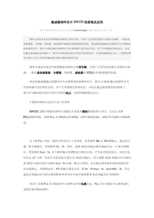
1 锁相环频率合成芯片及工作原理Si4133为数字锁相式频率合成器芯片的基本模块框图如图1所示。
它包含3路PLL(锁相环路)。
每路PLL由PD(相位检测器)、LF(环路滤波器)、VCO和可编程分频器构成。
以1路PLL为例,简要介绍该芯片工作原理。
参考频率fin从XIN脚输人,通过放大器、R分频器后,得到频率fin/R;同时,这路VCO的输出频率fout经过一个N分频器后,得到频率fout/N;2个频率输人到PD进行相位比较,产生误差控制电压,该误差电压经过LF可得一误差信号的直流分量作为VCO的输入,用于调整VCO的输出信号频率,使VCO分频后的信号频率fout/N向fin/R近于相等,直至最后两者频率相等而相位同步实现锁定。
环路锁定时,PD的输人频差为0,即fin/R=fout/N,fout=Nfin/R,可以通过改变输出信号的分频系数N和参考信号的分频系数R来改变输出信号的频率。
锁相环(PLL)频率合成调谐器

锁相环(PLL)频率合成调谐器调谐器俗称高频头,是对接收来的高频电视信号进行放大(选频放大)并通过内部的变频器把所接收到的各频道电视信号,变为一固定频率的图像中频(38MHz)和伴音中频以利于后续电路(声表面滤波器、中放等)对信号进行处理。
调谐器(高频头)原理:高频放大:把接收来的高频电视信号进行选频放大。
本机振荡器:产生始终高于高频电视信号图像载频38MHz的等幅载波,送往混频器。
混频器:把高频放大器送来的电视信号和本机振荡器送来的本振等幅波,进行混频产生38MHz的差拍信号(即所接收的中频电视信号)输出送往预中放及声表面滤波器。
结论:简单的说:只要改变本机振荡器的频率即可达到选台的目的)一、电压合成调谐器:早期彩色电视接收机大部分均采用电压合成高频调谐器,其调谐器的选台及波段切换均由CPU输出的控制电压来实现(L、H、U波段切换电压及调谐选台电压),其中调谐选台电压用来控制选频回路和本振回路的谐振频率,调谐选台电压的任何变化都将导致本机振荡器频率偏移,选台不准确、频偏、频漂。
为了保证本机振荡器频率频率稳定,必须加上AFT系统。
由于AFT系统中中放限幅调谐回路和移相网络一般由LC谐振回路构成,这个谐振回路是不稳定的,这就造成了高频调谐器本机振荡器频率不稳,也极易造成频偏、频漂。
二、频率合成调谐器1、频率合成的基本含义:是指用若干个单一频率的正弦波合成多个新的频率分量的方法(频率合成调谐器的本振频率是由晶振分频合成的)。
频率合成的方法有很多种。
下图为混频式频率合成器方框图以上图中除了三个基频外还有其“和频”及“差频”输出(还有各个频率的高次谐波输出)。
输出信号的频率稳定性由基准信号频率稳定性决定,而且输出信号频率误差等于各基准信号误差之和,因此要想减少误差除了要提高基准信号稳定度之外还应减少基准信号的个数。
2、锁相环频率合成器:其方框图类似于彩色电视接收机中的副载波恢复电路,只是在输入回路插入了一个基准信号分频器(代替色同步信号输入)而在反馈支路插入一个可编程分频器(代替900移相)。
CD4046锁相环设计频率合成器
目录一、设计和制作任务 (2)二、主要技术指标 (2)三、确定电路组成方案 (2)四、设计方法 (3)(一)、振荡源的设计 (3)(二)、N分频的设计 (3)(三)、1KHZ标准信号源设计(即M分频的设计) (4)五、锁相环参数设计 (5)六、参考文献 (6)附录:各芯片的管脚图 (6)锁相环CD4046设计频率合成器内容摘要:频率合成是以一个或少量的高准确度和高稳定度的标准频率作为参考频率,由此导出多个或大量的输出频率,这些输出的准确度与稳定度与参考频率是一致的。
在通信、雷达、测控、仪器表等电子系统中有广泛的应用,频率合成器有直接式频率合成器、直接数字式频率合成器及锁相频率合成器三种基本模式,前两种属于开环系统,因此是有频率转换时间短,分辨率较高等优点,而锁相频率合成器是一种闭环系统,其频率转换时间和分辨率均不如前两种好,但其结构简单,成本低。
并且输出频率的准确度不逊色与前两种,因此采用锁相频率合成。
关键词:频率合成器CD4046一、设计和制作任务1.确定电路形式,画出电路图。
2.计算电路元件参数并选取元件。
3.组装焊接电路。
4.调试并测量电路性能。
5. 写出课程设计报告书二、主要技术指标1.频率步进 1kHz2.频率稳定度f ≤1KHz3.电源电压 Vcc=5V三、确定电路组成方案原理框图如下,锁相环路对稳定度的参考振动器锁定,环内串接可编程的分频器,通过改变分频器的分配比N,从而就得到N倍参考频率的稳定输出。
晶体振荡器输出的信号频率f1,经固定分频后(M分频)得到基准频率f1’,输入锁相环的相位比较器(PC)。
锁相环的VCO输出信号经可编程分频器(N分频)后输入到PC的另一端,这两个信号进行相位比较,当锁相环路锁定后得到:f1/M=f1’=f2/N 故f2=Nf’1 (f’1为基准频率)当N变化时,或者N/M变化时,就可以得到一系列的输出频率f2。
四、设计方法(一)、振荡源的设计用CMOS与非门和1M晶体组成1MHz振荡器,如图14。
LMX2336锁相环频率合成器电路的设计及编程应用

nd a VCO c i r c u i t b a s e d o n L MX 2 3 3 6 i s g i v e n .T h e wa y u s i n g Ho t e l k p r o ra g m mi n g mi c r o c o n t r o l l e r HT 9 8 R 0 6 8 t o c o n t r o l
不 可 比拟 的 。L M X 2 3 3 6就 是这 样 一款 符合 设 计应 用
干扰 , 产 生频率 稳 定度 高 的射 频 载波 , 在 通信 传 输 中
【 摘
要】在无线 电收发设备 中, 锁相 频率合成器 电路是其不 可或缺 的组成部分。首先介绍 了美 国国家半导体公 司
生产 的低功耗 双 通 道 频率 合 成 器 L MX 2 3 3 6 的 内部 结 构 , 然 后在 深 入研 究其 应 用 特 点 的基 础 上 , 给 出 了基 于 L M X 2 3 3 6的外 围滤波器 和 V C O电路 的设 计, 以及利用合 泰单 片机 H T 9 8 R 0 6 8编 程控制 L MX 2 3 3 6来 达到调 整 V C O
基于ADF4157的Σ-△小数分频锁相环频率合成器设计

图 3 示 为 芯 片原 理 框 图 ,L D T 、E为 串行 输 入 时 所 C K、 A E L
相对较差 , 成度低 , 集 越来 越不能满足现代低成本 、 高一致性 、
钟数据和使能控制 ; X U MU O T为输 出信号锁定检测脚 ; P为电 C 荷泵输出。 中, S 其 C R为快锁功能控制 , 它可 以在小频率范围内 信号变换时 陕速锁定 ,它的原理是通过控制 C P输出电流来降
为 (R C2% v。 F A /2XFm
∞ m RⅡ s
式 ( 中第 一 项 为 所需 频 率 , 二 项 为 由小数 分频 形 成 的 1 ) 第
阶调 制 的量 化误 差 。
它将 前 一 级 的 量 化误 差作 为下 一 级 调制 器 的输 入 , 而把 从
噪声推 向远端 , 噪声在信号近端受到很大抑制 , 以被环路 使 可 滤波器滤除 , 从而达到更好的噪声整形效果 。因此 , 采用多阶调
快 速 发 展 , 高 频 率 、 定 度 的要 求 就 越 高 。 对 高稳
荡器输 出信号相位 , 出 两个信号相 位差成正 比的电压作为 取
误 差 电压 来 控 制 V O输 出频 率 , C 实现 稳 定 信 号 输 出 。
整数 分频锁相环频率 合成器存在 高分 辨率 低 噪声 之间
锁 相 式 、 锁 相 式 和 数字 分频 锁 相 式 三 种 。数 字 分 频 锁 相 环 取样
∑一 △小数分频锁相环频率合成器具有很高 的开关速度以 及通过 F G P A控制可以迅速 变频 ,有效地 抑制 了输 出杂散 , 有 效地解决了高鉴相频率和高分辨率的矛盾 , 降低 了输出信号的 相位噪声。 三阶 ∑一 b Al 数分频锁相环的结构 如图 l 所示 。
基于MC145162的锁相频率合成器的设计
此 芯片采 用 C MOS工艺 , 的最 高工作 频率 可 达到 它 6 0MHz ,内部包 括充 分可 编程 的接 收 、发送 、参考 和辅 助 参考 计数 器 ,它们 的存 取可 以通 过 一个 串行
j 魍
叛 德
图 1 锁相 式频率合成 器电路框 图
收稿 日期 :2 1 卜 2 0 卜0 9
作者简介:夏继媛 (9 9 ) 17 一 ,女,吉林人,讲师 ,硕士,主要研究方 向为嵌入式技术、无线通讯技术
2 0 1 2 压控 振 荡器 电路 ( O) . VC
深 圳 职业 技术 学 院学 报
路 的工作 原理 就 是将 2套独 立 VC 电路配 合锁 相 O
技术 是 一种相 位 负反 馈频 率控 制 技术 ,该 技术 在 锁定 时无 剩 余频 差 ,并具 有 良好 的窄 带载 波跟踪 性能 和带 宽调 制跟 踪性 能 ,而 且对 相位 噪 声和 杂
散也具有很好 的抑制作用 ,具有控制灵活、体积
( C ,其 工 作范 围为 3  ̄6 V O) 0 0MHz ,而 这 种 电
路 结构 在 高 频 到特 高频 ( " 0 z 3  ̄5 0 MH )范 围是 VC 的 主 要 结 构 形 式 之 一 , 其 特 点 是 容 易 起 O
振 . 同时 由于采 用 了共集 电极组 态 ,振 荡频 率可 做 到 较高 ,频率 稳定 度 也较好 .为 了方便 调 试 , 其 中 电感 采 用 自制 的 中周 .
pD
偏 置形 式 ,其 中 1 , 1 ,J7是偏 置 电阻 ,用 来 7 7 R 1 o 2 1 调 节三 极 管 Q1 的工作 点 电压 ,输 入 信号 从耦 合 电 6 3 容 c7输 入 ,放 大后 的信 号 由 C7输 出给 缓冲 、隔 1 2 1 1
锁相式数字频率合成器实验报告.
*******************实践教学*******************兰州理工大学计算机与通信学院2012年春季学期《通信系统基础实验》设计项目实验报告设计题目:锁相式数字频率合成器实验报告专业班级:设计小组名单:指导教师:陈昊目录一、设计实验目的 (3)二、频率合成基本原理 (4)2.1频率合成的概念 (4)2.2频率合成器的主要技术指标 (4)2.3锁相频率合成器 (5)三、锁相环技术 (6)3.1 锁相环工作原理 (6)3.2 锁相环CD4046芯片介绍 (6)四、基于锁相环技术的倍频器 (10)4.1 HS191芯片介绍 (10)4.2 基于锁相环技术的倍频器的设计 (12)4.2.1 工作原理 (12)3.2.2 Proteus软件仿真 (13)4.2.3 硬件实现 (14)4.2.4 锁相环参数设计 (15)五、总结与心得 (17)六、参考文献 (18)七、元器件清单 (19)一、设计实验目的1. 掌握VCO压控振荡器的基本工作原理。
2. 加深对基本锁相环工作原理的理解。
3. 熟悉锁相式数字频率合成器的电路组成与工作原理.。
二、频率合成基本原理2.1频率合成的概念频率合成是指由一个或多个频率稳定度和精确度很高的参考信号源通过频率域的线性运算,产生具有同样稳定度和精确度的大量离散频率的过程。
实现频率合成的电路叫频率合成器,频率合成器是现代电子系统的重要组成部分。
在通信、雷达和导航等设备中,频率合成器既是发射机频率的激励信号源,又是接收机的本地振荡器;在电子对抗设备中,它可以作为干扰信号放生器;在测试设备中,可作为标准信号源,因此频率合成器被人们称为许多电子系统的“心脏”。
早期的频率合成是用多晶体直接合成,以后发展成用一个高稳定参考源来合成多个频率。
20世纪50年代出现了间接频率合成技术。
但在使用频段上,直到50年代中期仍局限于短波范围。
60年代中期,带有可变分频的数字锁相式频率合成器问世。
锁相式频率合成器的设计与改进
电讯 技 术
T lc mmu iain En ie nn ee o nc t gn e g o
Vo . O No. 15 7
J1 0 0 u .2 1
文章 编号 :0 1 9 X 2 1 )7—0 1 0 10 —8 3 (0 00 10— 5
i a h r a 0 s y u igg i — o t l be a l e i uti up t o t h r be ta e i t s f s s s o t 8 n .B s an c nr l l mp i rc c i n o tu r ,te p o lm h tt ne i o s n oa i f r p h n t y
锁相 式频 率 合 成 器 的 设 计 与 改 进
马 宇 飞 , 署 坚 李
( 北京航空航天大学 电子信息工程学 院 , 北京 109 ) 0 11
摘 要 : 对 目前的锁 相式频 率合 成 器分辨 能力 不 高和频 率转换 时间较 长 的 问题 , 用 D S P L组 针 采 D/L 合式 频率合 成 器 , 号频 率 的转换 时 间最短 可达到 8 s 在输 出前 端采 用 增益 可 控放 大 电路 , 信 0n ; 有效
相式频率合成器 的设计方 法, 能有效提高输 出信号
的频 率分辨 能力 和 转换 时 间 ; 且 在 输 出端 提 出一 并
解决 了信号输出强度随着频率升高而不断衰减的问题 , 使输出信号幅度稳定在 1 . 间。详 ~10 v之 5
细论 述 了 系统 的总体 结构 、 软硬 件 结构 , 并给 出了实验 测 试结果 。 关键词 : 率合成 器 ; 相环 ; 频 锁 信号发 生 器 ; 增益 可控放 大器 中图分 类号 :N 4 . T 722 文献 标识码 : A di1 .9 9 ji n 10 —8 3 .0 0 0 .2 o:0 3 6 / . s .0 1 9 x2 1 .7 0 3 s
吞除脉冲式数字锁相频率合成器的设计
RE E F RE NC E OS ÷ R C
器实 现模 式变 换.
8 , , ) 、 为鉴 相信 号输 出端 , 出环 路误 差信 号. 否输 出及 输 出脉 冲宽度 取决 于鉴 相器 输 入信 号 - , 输 是 厂 R
厂 的相位 差. , , 厂 , v L 的波形 图如 图 2所示 . 、 , 、 R f , D ,
( 章 编 号 ] 1 7 — 0 7 2 1 ) 30 7 — 4 ( 图 分 类 号 ] 文 6 22 2 ( 0 1 0 — 0 8 0 中
TN7 2 ( 献 标 识 码 ] A 4 文
0 引 言
频 率合成 器 是现代 通信 设备 的重 要组 成部 分 , 率合 成 技术 是 将一 个 高稳 定 度 和 高准 确 度 的基 准 频 率 频 经过 四则 运算 , 生 同样 稳定 度 和准 确度 的任 意频率 . 保证 足 够小 的信道 间隔 和 比较 高 的 工作 频 率 , 采 产 为 可 用 先进 的吞 除脉 冲式数 字锁 相频 率合 成器 . 所谓 “ 除 脉 冲” 术 , 吞 技 就是 采 用 高速 双模 前 置 分 频器 , 根据 模 式 控 制 电平 的高低 , 来控 制它 的 分频 比为 P 或 P+ 1 摩 托 罗拉 公 司 生产 的 MC 4 1 22芯 片 是 一 种 先 进 的 . 1 5 5— P L可编 程频率 合 成器 , L 内部 具有 6位 吞除计 数 器. 种 P L可 编程 频率 合 成 器 的稳 定度 和 准确 度 与基 准 这 L 频 率相 当 , 额外误 差 , 无 在通 信领 域有 广泛 的应 用.
表 1 参 考 分 频 器 真 值 表
参 考 地 址 码
RA2 RA 1 R A0
- 1、下载文档前请自行甄别文档内容的完整性,平台不提供额外的编辑、内容补充、找答案等附加服务。
- 2、"仅部分预览"的文档,不可在线预览部分如存在完整性等问题,可反馈申请退款(可完整预览的文档不适用该条件!)。
- 3、如文档侵犯您的权益,请联系客服反馈,我们会尽快为您处理(人工客服工作时间:9:00-18:30)。
信息科学与技术学院通信原理课程设计课题名称:数字频带通信系统的建模与设计学生姓名:王太程2011508199学院:信息科学与技术学院专业年级:电子信息工程2011级指导教师:钟福如讲师完成日期:二○一四年七月十日目录第0章引言 (2)第1章 (4)1.1 设计任务要求及方案论证 (4)1.1.1 任务要求 (4)1.1.2 锁相环频率合成的原理 (4)1.1.3锁相环频率的合成与应用(调制与解调) (6)1.1.4锁相环在调制中的应用 (7)1.1.5 锁相环在解调中的应用 (8)1.1.6 锁相环在频率合成电路中的应用 (9)1.2 仿真工具SYSTEMVIEW简介 (9)1.3 电路的设计与调试 (10)1.3.1 三环式锁相环频率合成电路 (10)第2章 (12)2.1 仿真的结果及分析 (12)第3章 (14)参考文献 (15)第0章引言锁相环(Phase Lock Loop),简称PLL,是一种利用外部输入的参考信号控制环路内部振荡信号反馈控制电路。
他的被控制量是相位,被控对象是压控振荡器。
如果锁相环路中压控振荡器的输出信号频率发生变化,则输入到相位比较器的信号相位θv(t)和θR(t)必然会不同,使相位比较器输出一个与相位误差成比例的误差电压Vd(t),经环路滤波器输出一个缓慢变化的直流电压Vc(t),来控制压控振荡器输出信号的相位,使输入和输出相位差减小,直到两信号之间的相位差等于常数。
此时,压控振荡器的输出信号频率和输入信号频率相等,且环路处于锁定状态。
锁相环是构成频率合成器的核心部件。
主要由相位比较器(Phase Discriminator)、压控振荡器(Voltage Control Oscillator)、环路滤波器(Loop Filter)组成。
锁相环路是一个能跟踪输入信号相位的闭环自动控制系统。
锁相环路系统在各个领域都有很多的用途,发展将势不可挡。
锁相环路在宇宙飞行目标的跟踪、遥测和遥控、电视接收机、电动机转速控制、自动跟踪调谐等领域都有更好的发展。
频率合成是电子系统中的关键技术,是决定电子系统性能的主要设备,随着通信、数字电视、卫星定位、航空航天、雷达和电子对抗等技术的发展,频率合成技术提出了越来越高的要求。
频率合成技术是将一个或多个高稳定、高精确度的标准频率经过一定变换,产生同样高稳定度和精确度的大量离散频率的技术。
锁相环是一个相位反馈控制系统,在数字锁相环中,由于误差控制信号是离散的数字信号,而不是模拟电压,因而受控的输出电压的改变是离散的而不是连续的;此外,环路组成部件也全用数字电路实现,故而这种锁相环就称之为数字锁相环(Digital Phase Lock Loop)。
传统的锁相环由模拟电路实现,而数字锁相环与传统的模拟电路实现的PLL相比,具有精度高且不受温度和电压影响,环路带宽和中心频率编程可调,易于构建高阶锁相环等优点,并且应用在数字系统中时,不需A/D及D/A转换。
随着通讯技术、集成电路技术的飞速发展和系统芯片(SoC)的深入研究,数字锁相环必然会在其中得到更为广泛的应用。
近些年来, 由于大规模集成电路制造技术的广泛运用, 数字锁相环中的技术指标得到了很大的提高, 同时电路的体积也大大减小。
利用这些高性能的器件, 可以组成体积小、杂散分量低的频率合成器。
在许多电子设备中,常常需要产生多种频率且精度较高的信号,因此采用数字锁相环的频率合成器是一种比较实际可行的方法。
设计目的:加深对锁相式频率合成器的理解,了解解调方法以及每种解调方法的模块建立,熟练使用systemview仿真软件。
锻炼动手能力等等,为以后更好的踏入社会打下坚实的基础。
第1章1.1 设计任务要求及方案论证1.1.1 任务要求锁相式数字频率合成器设计1.1.2 锁相环频率合成的原理许多电子设备要正常工作,通常需要外部的输入信号与内部的振荡信号同步,利用锁相环路就可以实现这个目的。
锁相环路是一种反馈控制电路,特点是利用外部输入的参考信号控制环路内部振荡信号的频率和相位。
因锁相环可以实现输出信号频率对输入信号频率的自动跟踪,所以锁相环通常用于闭环跟踪电路。
锁相环在工作的过程中,当输出信号的频率与输入信号的频率相等时,输出电压与输入电压保持固定的相位差值,即输出电压与输入电压的相位被锁住,这就是锁相环名称的由来。
锁相环通常由鉴相器、环路滤波器和压控振荡器三部分组成,锁相环组成的原理框图如下图所示。
图1-1 锁相环原理图锁相环中的鉴相器又称为相位比较器,它的作用是检测输入信号和输出信号的相位差,并将检测出的相位差信号转换成UD(t)电压信号输出,该信号经低通滤波器滤波后形成压控振荡器的控制电压UC(t),对振荡器输出信号的频率实施控制。
锁相环中的鉴相器通常由模拟乘法器组成,利用模拟乘法器组成的鉴相器电路如图所示。
图1-2 鉴相器原理图鉴相器的工作原理是:设外界输入的信号电压和压控振荡器输出的信号电压分别为:(2-1) (2-2)式中的ω0为压控振荡器在输入控制电压为零或为直流电压时的振荡角频率,称为电路的固有振荡角频率。
则模拟乘法器的输出电压uD 为:(2-3)用低通滤波器LF 将上式中的和频分量滤掉,剩下的差频分量作为压控振荡器的输入控制电压uC (t )。
即uC (t )为:(2-4)式中的ωi 为输入信号的瞬时振荡角频率,θi(t)和θo(t)分别为输入信号和输出信号的瞬时位相,根据相量的关系可得瞬时频率和瞬时位相的关系为:(2-5)即:(2-6)则,瞬时相位差θd 为:(2-7)对两边求微分,可得频差的关系式为:(2-8)上式等于零,说明锁相环进入相位锁定的状态,此时输出和输入信号的频率和相位保持恒定不变的状态,uc(t)为恒定值。
当上式不等于零时,说明锁相环的相位还未锁定,输入信号fi和输出信号fo的频率不相等,uc(t)随时间而变。
因压控振荡器的压控特性如图2-3所示,该特性说明压控振荡器的振荡频率ωu以ω0为中心,随输入信号电压uc(t)的变化而变化。
该特性的表达式为:图1-3 压控振荡器压控特性上式说明当Uc(t)随时间而变时,压控振荡器的振荡频率ωu也随时间而变,锁相环进入“频率牵引”,自动跟踪捕捉输入信号的频率,使锁相环进入锁定的状态,并保持的状态不变。
1.1.3锁相环频率的合成与应用(调制与解调)调制,是对信号源的信息进行处理,使其变为适合于信道传输的形式的过程。
一般来说,信号源的信息(也称为信源)含有直流分量和频率较低的频率分量,称为基带信号。
基带信号往往不能作为传输信号,因此必须把基带信号转变为一个相对基带频率而言频率非常高的信号以适合于信道传输。
这个信号叫做已调信号,而基带信号叫做调制信号。
调制是通过改变高频载波的幅度、相位或者频率,使其随着基带信号幅度的变化而变化来实现的。
而解调则是将基带信号从载波中提取出来以便预定的接收者(也称为信宿)处理和理解的过程。
调制在通信系统中有十分重要的作用。
通过调制,不仅可以进行频谱搬移,把调制信号的频谱搬移到所希望的位置上,从而将调制信号转换成适合于传播的已调信号,而且它对系统的传输有效性和传输的可靠性有着很大的影响,调制方式往往决定了一个通信系统的性能。
在通信中,常常采用的调制方式有以下几种:对于模拟调制而言,主要有幅度调制(调幅AM,双边带调制DSB)和角度调制(调频,调相)两种。
对于数字调制而言,主要有脉冲调制(脉幅调制PAM,脉宽调制PWM等)以及增量调制DM等等。
1.1.4锁相环在调制中的应用调频,就是载频的频率不是一个常数,是随调制信号而在一定范围内变化,其幅值则是一个常数。
与其对应的,调幅就是载频的频率是不变的,其幅值随调制信号而变。
一般干扰信号总是叠加在信号上,改变其幅值。
所以调频波虽然爱到干扰后幅度上也会有变化,但在接收端可以用限幅器将信号幅度上的变化削去,所以调频波的抗干扰性极好,用收音机接收调频广播,基本上听不到杂音。
使载波频率按照调制信号改变的调制方式叫调频。
已调波频率变化的大小由调制信号的大小决定,变化的周期由调制信号的频率决定。
已调波的振幅保持不变。
调频波的波形,就像是个被压缩得不均匀的弹簧,调频波用英文字母FM表示。
调幅波的特点是频率与载波信号的频率相等,幅度随输入信号幅度的变化而变化;调相波的特点是幅度与载波信号的幅度相等,相位随输入信号幅度的变化而变化。
调幅波和调频波的示意图如下图所示。
图1-4 调幅波与调频波上图的(a)是输入信号,又称为调制信号;图(b)是载波信号,图(c)是调幅波和调频波信号。
解调是调制的逆过程,它可将调制波Uo还原成原信号Ui。
1.1.5 锁相环在解调中的应用调频波的特点是频率随调制信号幅度的变化而变化。
由2-8式可知,压控振荡器的振荡频率取决于输入电压的幅度。
当载波信号的频率与锁相环的固有振荡频率ωo相等时,压控振荡器输出信号的频率将保持ωo不变。
若压控振荡器的输入信号除了有锁相环低通滤波器输出的信号uc外,还有调制信号ui,则压控振荡器输出信号的频率就是以ωo为中心,随调制信号幅度的变化而变化的调频波信号。
由此可得调频电路可利用锁相环来组成,由锁相环组成的调频电路组成框图如图2-5所示。
[1]图1-5 锁相环调频电路根据锁相环的工作原理和调频波的特点可得解调电路组成框图如图2-6所示。
图1-6 锁相环调频波解调电路1.1.6 锁相环在频率合成电路中的应用在现代电子技术中,为了得到高精度的振荡频率,通常采用石英晶体振荡器。
但石英晶体振荡器的频率不容易改变,利用锁相环、倍频、分频等频率合成技术,可以获得多频率、高稳定的振荡信号输出。
输出信号频率比晶振信号频率大的称为锁相倍频器电路;输出信号频率比晶振信号频率小的称为锁相分频器电路。
锁相倍频和锁相分频电路的组成框图所示。
图中的N大于1时,为分频电路;当0<N<1时,为倍频电路[1]。
图1-7 锁相环频率合成器1.2 仿真工具SYSTEMVIEW简介SystemView是美国ELANIX公司推出的,基于Windows环境下运行的用于系统仿真分析的可视化软件工具,它使用功能模块(Token)去描述程序,无需与复杂的程序语言打交道,不用写一句代码即可完成各种系统的设计与仿真,快速地建立和修改系统、访问与调整参数,方便地加入注释。
利用System View ,可以构造各种复杂的模拟、数字、数模混合系统,各种多速率系统,因此,它可用于各种线性或非线性控制系统的设计和仿真。
用户在进行系统设计时,只需从System View 配置的图标库中调出有关图标并进行参数设置,完成图标间的连线,然后运行仿真操作,最终以时域波形、眼图、功率谱等形式给出系统的仿真分析结果。
1.3 电路的设计与调试1.3.1 三环式锁相环频率合成电路三环式锁相环由三个锁相环构成,如图所示。