电子技术基础chapter1
中职《电子技术基础》第四版电子教案

电路搭建
根据实验要求,选择合适的电子元件搭建电路。
实验操作步骤与注意事项
实验结果的分析与总结
数据整理
将实验数据整理成表格或图表,便于分析。
结果分析
根据实验数据,分析电路性能,验证电子技术的基本原理。
总结归纳
总结实验过程中的经验和教训,为后续的实验和实践提供参考。
THANKS
感谢您的观看。
应用实例2
非门可以用于实现逻辑非运算,例如实现信号的反相等。
应用实例3
逻辑门电路的应用实例
05
CHAPTER
电子技术实践
通过实验,使学生能够深入理解电子技术的基本原理,为后续的学习和实践打下坚实的基础。
掌握电子技术的基本原理
培养实践操作能力
提高问题解决能力
培养团队协作精神
实验是培养学生实践操作能力的重要途径,通过实验,学生能够掌握电子设备的基本操作和调试技能。
03
CHAPTER
模拟电子技术
模拟信号是连续变化的物理量,如声音、光线、温度等。模拟电路则是用于处理模拟信号的电子电路。
模拟信号
模拟电路通常由电阻、电容、电感等元件组成,具有连续的输入输出关系,能够实现信号的放大、滤波、振荡等功能。
模拟电路的特点
模拟电路广泛应用于通信、音频、视频、测量和控制等领域。
数字电路
数字电路是处理数字信号的电路,由逻辑门、触发器等基本逻辑单元组成,具有高可靠性、高稳定性等特点。
数字信号与数字电路
工作原理
逻辑门电路是数字电路的基本单元,其工作原理基于逻辑代数,实现逻辑运算和逻辑控制功能。
分类
按照逻辑功能的不同,逻辑门电路可以分为与门、或门、非门、与非门、或非门等类型。
英文版模拟电子技术课件第一章

Introduction of The Course
• Program of the course About 2-8th weeks:analog section About 9-15th weeks:digital section
Intrinsic materials are those semiconductors that have been carefully refined to reduce the impurities to a very low levelessentially as pure as can be made available through modern technology.
the main object in this course
SEMICONDUCTOR MATERIALS
Semiconductors are a special class having a conductivity between that of a good conductor and that of an insulator.the three semiconductors used most frequently in the construction of electronic devices are germanium-Ge,silicon-Si and gallium arsenide-GaAs.
si
GGee
silicon
germanium
Chapter 1 Semiconductor Diodes
1.2 Semiconductor Materials 1.3 intrinsic Semiconductor 1.4 Extrinsic Semiconductor 1.5 Semiconductor Diode 1.7 Resistance Levels 1.8 Diode Equivalent Circuits
模拟电子技术课件-简介导论

分析是为实现综合而积累知识和经验的过程。
6
Microelectronics Circuit Analysis and Design
Prologue to Analog Electronics
Electronics is defined as the science of the motion of charges in a gas, vacuum, or semiconductor.
Electronic Circuits Amplifiers
Notation
Prologue to Electronics 6.1 Analog Signals and Linear Amplifiers 6.3 Basic Amplifier Configurations
10
Amplifiers
(1) 课程性质与教学目标 (2) 课程内容与教学安排 (3) 关键词与核心内容 (4) 模电课程特点与学习方法 (5) 参考资源 (6) 考核与答疑
电类专业的一门技术基础课
Amplifiers
工程性质、 实践性很强
Operational Amplifiers (Op-Amp)
Transistor BJT
(4h) (4h)
(12h)
(4h)
(4h) (4h) 运放 内部电路 (6h)
(7h) (7h) (共52h)
《高频电子技术》课件

THANKS
谢谢
在此添加您的文本16字
带阻滤波器允许除某一频段外的信号通过,抑制该频段信 号。
滤波器的性能指标
通带和阻带性能
插入损耗
通带和阻带的边缘频率、带宽等参数决定 了滤波器的频率选择性和抑制能力。
滤波器对有用信号的衰减程度,以dB为单 位表示。
群时延
稳定性
滤波器对信号相位变化的量度,反映信号 通过滤波器的速度。
振荡原理
高频电子电路中的元件通 过正反馈和负反馈等机制 ,产生振荡信号,实现信 号的调制和解调等功能。
传输线原理
高频电子电路中的信号传 输遵循传输线理论,信号 在传输过程中会受到线路 的分布参数影响。
03
CHAPTER
高频电子技术中的放大器
放大器的分类与特点
分类
按功能可以分为电压放大器、功率放 大器、跨导放大器等;按频率可分为 低频放大器、高频放大器、微波放大 器等。
特点
高频放大器具有较高的增益和带宽, 能够放大微弱的高频信号;低频放大 器具有较低的噪声系数和较好的线性 度,适用于放大低频信号。
放大器的性能指标
增益
放大器的输出信号幅度与输入信号幅 度之比,反映了放大器的放大能力。
带宽
放大器能够正常工作的频率范围,反 映了放大器的频率响应能力。
线性度
放大器在小信号和大信号输入下的性 能差异,反映了放大器的失真程度。
频率范围
高频电子电路的工作频率范围,通常指几百 千赫兹到几百兆赫兹。
带宽
高频电子电路的频率响应范围,通常指电路 能够正常工作的频率范围。
增益
高频电子电路的放大倍数,用于衡量电路的 放大能力。
噪声系数
高频电子电路的噪声与信号比值,用于衡量 电路的噪声性能。
【2024版】微电子封装技术课程重点内容(English)

Microelectronics packaging technology(R eview contents)Chapter 1:Introduction1.The development characteristics and trends of microelectronics packaging.2.The functions of microelectronics packaging.3.The levels of microelectronics packaging technology.4.The methods for chip bonding.Chapter 2:Chip interconnection technologyIt is one of the key chapters1.The Three kinds of chip interconnection, and their characteristics and applications.2.The types of wire bonding (WB) technology, their characteristics and working principles.3.The working principle and main process of the wire ball bonding.4.The major materials for wire bonding.5.Tape automated bonding (TAB) technology:1)The characteristic and application of TAB technology.2)The key materials and technologies of TAB technology.3)The internal lead and outer lead welding technology of TAB technology.6. Flip Chip Bonding (FCB) Technology1)The characteristic and application of flip chip bonding technology2)UBM and multilayer metallization under chip bump;UBM’s structure and material, and the roles ofeach layer.3)The main fabrication method of chip bumps.4)FCB technology and its reliability.5)C4 soldering technology and its advantages.6)The role of underfill in FCB.7)The interconnection principles for Isotropic and anisotropic conductive adhesive respectively. Chapter 3: Packaging technology of Through-Hole components1.The classification of Through-Hole components.2.Focused on:DIP packaging technology, including its process flow.3.The characteristics of PGA.Chapter 4:Packaging technology of surface mounted device (SMD)1.The advantages and disadvantages of SMD.2.The types of SMD.3.The main SMD packaging technologies, focused on:SOP、PLCC、LCCC、QFP.4.The packaging process flow of QFP.5.The risk of moisture absorption in plastic packages, the mechanism of the cracking caused by moistureabsorption, and solutions to prevent for such failure.Chapter 5:Packaging technology of BGA and CSP1.The characteristics of BGA and CSP.2.The packaging technology for PBGA,and its process flow.3.The characteristics of packaging technology for CSP.4.The reliability problems of BGA and CSP.Chapter 6:Multi-Chip Module(MCM)1.The classification and characteristics of MCM2. The assembly technology of MCM.Chapter 7:Electronic packaging materials and substrate technology1. The classification of the materials for electronic packaging, the main requirements for packagingmaterials.2. The types of metals in electronic packaging, and their main applications.3. The main requirements for polymer materials in electronic packaging.4.Classification of main substrate materials, and the major requirements for substrate materials.Chapter 8:Microelectronics packaging reliability1.The basic concepts of electronic packaging reliability.2.The basic concepts for failure mode and failure mechanism in electronic packaging.3.Main failure (defect) modes (types) of electronic packaging.4.The purpose and procedure of failure analysis (FA) ;Common FA techniques (such as cross section, dyeand pry, SEM, CSAM ...).5 The purpose and key factors (such as stress level, stress type …) to design accelerated reliability test. Chapter 9:Advanced packaging technologies1.The concept of wafer level packaging (WLP) technology.2.The key processes of WL-CSP.3.The concept and types of the 3D packaging technologies.Specified Subject 1:LED packaging technology1. Describe briefly the four ways to achieve LED white light, and how they are packaged?2. Describe briefly the difference and similar aspects (similarity) between LED packaging andmicroelectronics packaging.3. And also describe briefly the development trend for LED package technology and the whole LED industryrespectively.Specified Subject 2:MEMS packaging technology1.The differences between micro-electro-mechanical system (MEMS) packaging technology and theconventional microelectronics packaging technologies.2.The function requirements of MEMS packaging.Extra requirement:The common used terms (Abbreviation) for electronic packaging.。
电工电子技术基础课程建设

加强团队合作
03
鼓励教师之间的合作与交流,共同研究教学方法和教学内容,
提高教学效果。
建立教学质量监控机制
定期进行教学检查
组织专家对教学情况进行定期检查,发现问题及时整改,确保教学 质量。
收集学生反馈意见
通过问卷调查、座谈会等方式收集学生对教学的意见和建议,及时 调整教学方法和内容,满足学生的需求。
网络教学资源开发
网络课程建设
建设电工电子技术基础网络课程,提供丰富的教学资源和学习工 具,方便学生自主学习和复习。
教学视频制作
制作电工电子技术基础教学视频,突出重点和难点,帮助学生更好 地理解和掌握课程内容。
在线测试与答疑
开发在线测试系统,方便学生进行自我检测和巩固所学知识;设立 在线答疑平台,及时解答学生学习中遇到的问题。
布置适量的作业,定期进行检查和评分,同时制 定合理的考试方式和评分标准,确保学生能够全 面掌握所学知识。
加强师资队伍建设
提高教师的教学水平
01
鼓励教师参加各种培训、学术交流活动,不断更新教育观念,
提高教学水平。
建立激励机制
02
对在教学工作中表现突出的教师进行表彰和奖励,激发教师的
教学热情和积极性。
模式。
翻转课堂
02 学生在课前预习,课堂上通过讨论、互动等方式深化
理解。
项目驱动教学
03
以实际问题或项目为导向,组织学生进行探究和实践
。
加强实践教学环节
01
实验教学改革
更新实验内容,增加综合性、设 计性实验,培养学生实践能力和 创新意识。
校企合作
02
03
课外科技活动
与企业合作,建立校外实习基地 ,开展实习实训活动,培养学生 工程实践能力。
电气工程及其自动化专业必备知识
电气工程及其自动化专业必备知识Chapter 1:电气工程基础知识⑴电流、电压和电阻⑵电路基础和欧姆定律⑶串并联电路的分析⑷电源和电能⑸电磁场基础知识Chapter 2:电路分析与设计⑴直流电路分析⑵交流电路分析⑶功率与功率因数校正⑷谐振电路设计与分析⑸数字电路设计基础Chapter 3:电机与变压器⑴三相交流电机⑵单相交流电机⑶直流电机⑷传感器与执行器⑸变压器基础知识与应用Chapter 4:电力系统与配电⑴电力系统概述⑵发电与变电⑶输电与配电系统⑷电力负荷管理⑸电能质量与调节Chapter 5:自动控制系统⑴控制系统基础⑵反馈控制系统⑶ PID 控制器⑷离散时间控制系统⑸自动化系统与工业控制Chapter 6:电气安全与规范⑴电气安全基础知识⑵国家电气安全法规与标准⑶高压电器安全操作⑷电气事故预防措施⑸地线与接地系统Chapter 7:电气测试与测量⑴仪器与测量误差⑵电气量测量⑶准确度和置信度⑷频谱分析仪与示波器⑸电气信号处理与测试工具Chapter 8:现代电气工程技术⑴电力电子技术⑵光伏与风能发电⑶电动汽车技术⑷智能电网与电力交易⑸在电气工程中的应用附件:⒈实验报告范例⒉电路设计案例⒊自动控制系统仿真软件教程⒋电气安全操作手册⒌测量仪器使用指南法律名词及注释:⒈电力法:是对电力工业进行管理和监督的法律法规。
⒉电力安全法:是为保障电力生产、供应、消费等环节的安全而制定的法律法规。
⒊电力负荷管理条例:是对电力系统负荷进行合理安排和管理的相关规定。
⒋地线:用于将设备或系统与地面接地连接的线路。
⒌接地系统:用于保护电气设备和人员免受电击的系统。
附件:⒈实验报告范例:[文件]⒉电路设计案例:[文件]⒊自动控制系统仿真软件教程:[文件]⒋电气安全操作手册:[文件]⒌测量仪器使用指南:[文件]法律名词及注释:⒈电力法:根据国家法律关于电力工业的规定。
⒉电力安全法:根据国家法律关于电力安全的规定。
⒊电力负荷管理条例:根据国家法律关于电力负荷管理的规定。
四川大学英语课程描述 Basics of Analog Electronic Technology 模拟电子技术基础
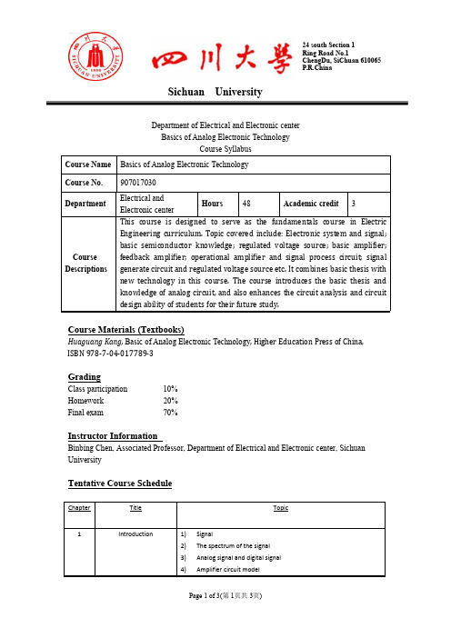
Sichuan UniversityP.R.ChinaDepartment of Electrical and Electronic centerBasics of Analog Electronic TechnologyCourse SyllabusCourse Name Basics of Analog Electronic TechnologyCourse No.907017030Department Electrical andElectronic centerHours48Academic credit3Course Descriptions This course is designed to serve as the fundamentals course in Electric Engineering curriculum.Topic covered include:Electronic system and signal; basic semiconductor knowledge;regulated voltage source;basic amplifier; feedback amplifier;operational amplifier and signal process circuit;signal generate circuit and regulated voltage source etc.It combines basic thesis with new technology in this course.The course introduces the basic thesis and knowledge of analog circuit,and also enhances the circuit analysis and circuit design ability of students for their future study.Course Materials(Textbooks)Huaguang Kang,Basic of Analog Electronic Technology,Higher Education Press of China, ISBN978-7-04-017789-3GradingClass participation10%Homework20%Final exam70%Instructor InformationBinbing Chen,Associated Professor,Department of Electrical and Electronic center,Sichuan UniversityTentative Course ScheduleChapter Title Topic1Introduction1)Signal2)The spectrum of the signal3)Analog signal and digital signal4)Amplifier circuit modelSichuan UniversityP.R.China5)The main performance indexes of Amplifier circuit2Operational amplifier1)Integrated circuit operational amplifier2)ideal operational amplifier3)Basic linear amplifier circuit4)Other applications of Noninverting input and invertinginput amplifier circuit5)The examples of SPICE simulation3Diode1)Semiconductor2)Formation and characteristics of P-N junction3)Diode4)analytical methods of diode basic circuit5)Special diode6)The examples of SPICE simulation4BJT and its amplifiercircuit 1)BJT2)common-emitter amplifier circuit3)analytical methods of amplifier circuit4)the Stability of static work point of the amplified circuits5)common-collector and common-base amplifier circuit6)combination amplify circuit7)Frequency response of amplifier circuit8)transient response of Single stage amplifier circuit9)The examples of SPICE simulation5Mosfet amplifier circuit1)MOSFET2)MOSFET amplifier circuit3)JFET4)MESFET5)Comparison of Circuit performances6)The examples of SPICE simulation6Analogue integratedcircuit 1)Biasing technique2)Differential amplifier3)transmission characteristics of Differential amplifier4)Integrated circuit operational amplifier5)major parameters of Integrated circuit operational amplifier6)Variable transconductance analog multiplier7)Noise and interference8)The examples of SPICE simulation7Feedback amplifier circuit1)The basic concept and classification of Feedback2)Four configurations of Negative feedback amplifier circuit3)Gain of Negative feedback amplifier circuit4)The influence of the negative feedback on amplifier circuitSichuan UniversityP.R.China5)Depth negative feedback6)Design of Negative feedback amplifier circuit7)Frequency response of Negative feedback amplifier circuit8)The stability of Negative feedback amplifier circuit9)The examples of SPICE simulation8Power amplifier circuit1)general issues of Power amplifier circuit2)emitter follower3)Integrated power amplifier4)The examples of SPICE simulation9signal processingand signal circuit 1)The basic concept and classification of filter circuit2)First order active filter circuit3)High order active filter circuit4)Switched Capacitor Filter5)Oscillating conditions of Sinusoidal oscillator circuit6)RC sinusoidal oscillator circuit7)LC sinusoidal oscillator circuit8)voltage comparator,Astable Multivibrator and Sawtooth wavegenerating circuit9)The examples of SPICE simulation10DC stabilized powersupply 1)Low power rectifier filter circuit2)series feed voltage regulator circuit3)switch voltage-stabilizing circuit4)The examples of SPICE simulation11computer aided analysisand design 1)SPICE program aided analysis of Electronic circuit2)SPICE program aided design of Electronic circuit。
- 1、下载文档前请自行甄别文档内容的完整性,平台不提供额外的编辑、内容补充、找答案等附加服务。
- 2、"仅部分预览"的文档,不可在线预览部分如存在完整性等问题,可反馈申请退款(可完整预览的文档不适用该条件!)。
- 3、如文档侵犯您的权益,请联系客服反馈,我们会尽快为您处理(人工客服工作时间:9:00-18:30)。
负载:
(发出功率);
U、I 实际方向相同,即电流从“-”端流出。 (吸收功率)。
2. 根据 U、I 的参考方向判别
U、I 参考方向相同,P =UI 0,负载;
P = UI 0,电源。
U、I 参考方向不同,P = -UI 0,负载; P = -UI 0,电源。
总目录 章目录 返回 上一页 下一页
b 若 U= –5V,则电压的实际方向 从 b 指向 a 。
在参考方向选定后,电流 ( 或电压 ) 值才有正负
之分。
总目录 章目录 返回 上一页 下一页
1.4 欧姆定律
U、I 参考方向相同时, U、I 参考方向相反时,
+
U=IR
+
U = – IR
U IR
U
–
–
表达式中有两套正负号:
IR
① 式前的正负号由U、I 参考方向的关系确定;
第1章 电路的基本概念与基本定律
1.1 电路的作用与组成部分 1.2 电路模型 1.3 电压和电流的参考方向 1.4 欧姆定律 1.5 电源有载工作、开路与短路 1.6 基尔霍夫定律 1.7 电路中电位的概念及计算
总目录 章目录 返回 上一页 下一页
第1章 电路的基本概念与基本定律
本章要求: 1.理解电压与电流参考方向的意义; 2. 理解电路的基本定律并能正确应用; 3. 了解电路的有载工作、开路与短路状态,
o
U/V
线性电阻的伏安特性
总目录 章目录 返回 上一页 下一页
1.5 电源有载工作、开路与短路
1.5.1 电源有载工作
I
开关闭合,接通
E
电源与负载
U
R
特征:
R0
I
E
I R0 R
① 电流的大小由负载决定。
U = IR 负载端电压 或 U = E – IR0
U
电源的外特性
② 在电源有内阻时,I U 。
组合来模拟实际电路中的器件,从而构成与实际电路
相对应的电路模型。
理想电路元件主要有
手电筒的电路模型
电阻元件、电感元件、
I
电容元件和电源元件等。 + +
例:手电筒
E
–U
手电筒由电池、灯 Ro
泡、开关和筒体组成。
–
电池
S 开关
导线
R 灯泡
总目录 章目录 返回 上一页 下一页
手电筒的电路模型
I
++
E
–U
b
或 I2 R2+I3 R3 –E2 = 0
基尔霍夫电压定律(KVL) 反映了电路中任一
回路中各段电压间相互制约的关系。
总目录 章目录 返回 上一页 下一页
注意:
1.列方程前标注回路循行方向;
2.应用 U = 0列方程时,项前符号的确定:
如果规定电位降取正号,则电位升就取负号。
3. 开口电压可按回路处理
电灯 电动机 电炉
...
话筒 放 扬声器 大 器
总目录 章目录 返回 上一页 下一页
2. 电路的组成部分
电源: 提供 电能的装置
发电机
升压 变压器
输电线
负载: 取用 电能的装置
降压 变压器
电灯 电动机
电炉
...
中间环节:传递、分 配和控制电能的作用
总目录 章目录 返回 上一页 下一页
2.电路的组成部分
(1)电位值是相对的,参考点选取的不同,电路中 各点的电位也将随之改变;
(2) 电路中两点间的电压值是固定的,不会因参考 点的不同而变, 即与零电位参考点的选取无关。
理解电功率和额定值的意义; 4. 会计算电路中各点的电位。
总目录 章目录 返回 上一页 下一页
1.1 电路的作用与组成部分
电路是电流的通路,是为了某种需要由电工设备 或电路元件按一定方式组合而成。
1. 电路的作用 (1) 实现电能的传输、分配与转换
发电机
升压 输电线 降压
变压器
变压器
(2)实现信号的传递与处理
Ro
–
电池
S 开关
导线
R 灯泡
今后分析的都是指电 路模型,简称电路。在 电路图中,各种电路元 件都用规定的图形符号 表示。
电池是电源元件,其 参数为电动势 E 和内阻 Ro;
灯泡主要具有消耗电能 的性质,是电阻元件,其 参数为电阻R;
筒体用来连接电池和灯 泡,其电阻忽略不计,认 为是无电阻的理想导体。
② U、I 值本身的正负则说明实际方向与参考
方向之间的关系。
通常取 U、I 参考方向相同。
总目录 章目录 返回 上一页 下一页
例:应用欧姆定律对下图电路列出式子,并求电阻R。
+
UI 6V 2A
R
– (a)
+
U 6V
I R
– –2A
(b)
解:对图(a)有, U = IR 所以 : R U 6 3Ω I2
(3) 实际方向与参考方向的关系
实际方向与参考方向一致,电流(或电压)值为正值;
实际方向与参考方向相反,电流(或电压)值为负值。
例: I aR b
+U–
若 I = 5A,则电流从 a 流向 b;
若 I = –5A,则电流从 b 流向 a 。 若 U = 5V,则电压的实际方向 从 a 指向 b;
aR 注意:
1.定律 在任一瞬间,从回路中任一点出发,沿回路循行
一周,则在这个方向上电位升之和等于电位降之和。
在任一瞬间,沿任一回路循行方向,回路中各
段电压的代数和恒等于零。 即: U = 0
I1 a I2
对回路1:E1 = I1 R1 +I3 R3
R1
R2
或 I1 R1 +I3 R3 –E1 = 0
E1 1 I3 R3 2 E2 对回路2:I2 R2+I3 R3=E2
对图(b)有, U = – IR 所以 : R U 6 3Ω I 2
总目录 章目录 返回 上一页 下一页
线性电阻的概念:
遵循欧姆定律的电阻称为线性电阻,它表示该段 电路电压与电流的比值为常数。
即:R U 常数 I
电路端电压与电流的关系称为伏安特性。线性电阻的伏安特性来自I/A是一条过原点的直线。
P = PE – P
UI = EI – I²Ro
负载 电源 内阻 ③ 电源输出的功率由负载决定。
取用 产生 消耗 负载大小的概念:
功率 功率 功率
负载增加指负载取用的
电流和功率增加(电压一定)。
总目录 章目录 返回 上一页 下一页
电源与负载的判别
1. 根据 U、I 的实际方向判别
电源: U、I 实际方向相反,即电流从“+”端流出,
b 设 b为参考点,即Vb=0V Va = Uab=10×6 = 60 V Vc = Ucb = E1 = 140 V
Vd = Udb =E2 = 90 V Uab = 10×6 = 60 V Ucb = E1 = 140 V
Udb = E2 = 90 V
总目录 章目录 返回 上一页 下一页
结论:
结点处各支路电流间相互制约的关系。
总目录 章目录 返回 上一页 下一页
2.推广
电流定律可以推广应用于包围部分电路的任一 假设的闭合面。
例:
IA
A
广义结点
I =? I
IB IC B
C
5
6V+_ 1
2
+_12V 1 5
IA + IB + IC = 0
I= 0
总目录 章目录 返回 上一页 下一页
1.6.2 基尔霍夫电压定律(KVL定律)
信号处理:
信号源:
放大、调谐、检波等
提供信息 话筒
放 扬声器
大
器
直流电源:
负载
提供能源
直流电源
电源或信号源的电压或电流称为激励,它推动电路 工作;由激励所产生的电压和电流称为响应。
总目录 章目录 返回 上一页 下一页
1. 2 电路模型
为了便于用数学方法分析电路,一般要将实际电路 模型化,用足以反映其电磁性质的理想电路元件或其
过载(超载): I > IN ,P > PN (设备易损坏) 欠载(轻载): I < IN ,P < PN (不经济)
总目录 章目录 返回 上一页 下一页
1.5.2 电源开路
开关 断开 特征:
I=0
I
E
Ro
U0
U = U0 = E 电源端电压 ( 开路电压 )
P = 0 负载功率
有I
电路中某处断开时的特征:
总目录 章目录 返回 上一页 下一页
2. 举例
c 20 a 5 d
求图示电路中 各点的电位:Va、 E1 Vb、Vc、Vd 。 140V
4A 6
6A
10A
E2
90V
解:
设 a为参考点, 即Va=0V Vb=Uba= –10×6= 60V Vc=Uca = 4×20 = 80 V Vd =Uda= 6×5 = 30 V Uab = 10×6 = 60 V Ucb = E1 = 140 V Udb = E2 = 90 V
电气设备的额定值 额定值: 电气设备在正常运行时的规定使用值 1. 额定值反映电气设备的使用安全性; 2. 额定值表示电气设备的使用能力。 例:灯泡:UN = 220V ,PN = 60W
电阻: RN = 100 ,PN =1 W 电气设备的三种运行状态
额定工作状态: I = IN ,P = PN (经济合理安全可靠)
源
1. 开路处的电流等于零;