按键扫描与LED显示驱动芯片ET6218R芯片资料
EXC2618
正常工作范围(Ta = -20 ~ +70℃,Vss = 0 V) 参数 逻辑电源电压 高电平输入电压 低电平输入电压 符号 VDD VIH VIL 最小 4.5 0.8 VDD 0 典型 5 最大 5.5 VDD 0.3 VDD 单位 V V V 测试条件 -
电气特性(Ta = -20 ~ +70℃,VDD = 4.5 ~ 5.5 V, Vss = 0 V, 参数 高电平输出电流 符号 Ioh1 Ioh2 低电平输出电流 低电平输出电流 IOL1 Idout 最小 -30 -35 150 4 典型 -35 -40 170 第 10 页
第 5 页
LED 驱动控制电路EXC2618
—————— 广州精芯科技有限公司
(3) 地址设定: 该指令用来设置显示寄存器的地址。 MSB 1 1 LSB b0 地址(00H~0DH) 如果地址设为 0EH 或更高,数据被忽略,直到有效地址被设定。 上电时,地址设为 00H。
—
—
b3
b2
b1
无关项
* 时序特性(Ta = -20 ~ +70℃,VDD = 4.5 ~ 5.5 V)
第 11 页
LED 驱动控制电路EXC2618 —————— 广州精芯科技有限公司
参数 时钟脉冲宽度 选通脉冲宽度 数据建立时间 数据保持时间 CLK → STB 时间 等待时间
符号 PWCLK PWSTB tSETUP tHOLD tCLK STB tWAIT
GND COM1 COM2 GND COM3 COM4 GND VDD SEG13/COM5 SEG12/COM6 SEG11/COM7 SEG10/KS10 SEG9/KS9 SEG8/KS8
第 2 页
创维8R61维修手册
本手册仅供有经验的维修人员使用,不适用于一般消费者,手册中没有对非技术人员企图维修本产品 而存在的潜在危害提出警告或提醒。
电器产品应由有经验的专业技术人员进行维护和修理,任何其它人企 图对本手册涉及的产品进行维护和修理将有可能受到严重伤害甚至有生命危险。
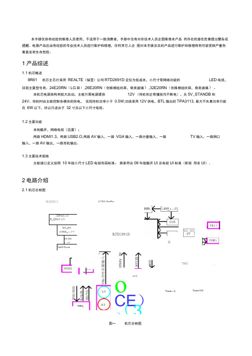
1产品综述1.1机芯概述8R61 机芯主芯片采用 REALTE (瑞昱)公司RTD2691D 定位为低成本,小尺寸带网络功能的LED 电视,目前主要型号有:24E20RN (LG 屏),26E20RN (创维模组所屏,奇美玻璃),32E20RN (创维模组所屏,奇美玻璃)。
本机芯电源架构有较大改动,主板只需电源提供12V (待机和正常播放均不断电),无5V_STANDB 和24V 。
待机时由主板控制各模块的供电, 实现待机功率小于 0.5W;功放采用12V 供电,BTL 输出的TPA3113, 最大不失真功率只能在 6W 以下,所以只适合于 32寸及以下小尺寸电视。
1.2主要功能本地酷开,网络电视(迅雷);两路HDMI1.3,两路USB2.O,两路AV 输入,一路 VGA 输入,一路分量输入,一路TV 输入,一路网口输入,一路AV 输出,一路耳机输出。
1.3主要技术规格主板接口定义按照 10年版小尺寸LED 电视布局标准,菜单符合09年版酷开UI 及电视UI 标准(即采 用老UI )。
2电路介绍2.1机芯总框图图一机芯总框图LVDS OuuPut5DPA3113(E_QKM 12vDC_DC i2ORE_l a 3 VDC DC 3 . SVNANI FlashRTD2691DoCE )(3)AVI7805|Tuner l 盘——Tuner I2C电游按口I lVGADDR 1 ・ SVDDR二2.2机芯新电路(本机芯特有)1,待机12V 关断电路:图二 待机12V 电源关断电路如图二 所示,C0N12V^ POWER_ElN 号控制。
当正常工作时, POWER_EN 高,Q21导通,Q20的GS 电压在-10V 左右,Q20导通,C0N_12\有电压输出,反之,待机时POWER_EN 低,C0N_12\关断。
LED显示屏专用驱动芯片详细介绍

目前,LED显示屏专用驱动芯片生产厂家主要有TOSHIBA(东芝)、TI(德州仪器)、SONY(索尼)、MBI{聚积科技}、SITI(点晶科技)等。
在国内LED显示屏行业,这几家的芯片都有应用。
TOSHIBA产品的Xing价比较高,在国内市场上占有率也最高。
主要产品有TB62705、TB62706、TB62725、TB62726、TB62718、TB62719、TB62727等。
其中TB62705、TB62725是8位源芯片,TB62706、TB62726是16位源芯片。
TB62725、TB62726分别是TB62705、TB62706的升级芯片。
这些产品在电流输出误差(包括位间和片间误差)、数据移位时钟、供电电压以及芯片功耗上均有改善。
作为中档芯片,目前”TB62725、TB62726已经逐渐替代了TB62705和TB62706。
另外,TB62726还有一种窄体封装的TB62726AFNA芯片,其宽度只有6.3mm(TB62706的贴片封装芯片宽度为8.2mm),这种窄体封装比较适合在点间距较小的显示屏上使用。
需要注意的是,AFNA封装与普通封装的引脚定义不一样(逆时针旋转了90度)。
TB62718、TB62719是TOSHIBA针对高端市场推出的驱动芯片,除具有普通恒流源芯片的功能外,还增加了256级灰度产生机制(8位PWM)、内部电流调节、温度过热保护(TSD)及输出开路检测(LOD)等功能。
此类芯片适用于高端的LED全彩显示屏,当然其价格也不菲。
TB62727为TOSHIBA的新产品,主要是在TB62726基础上增加了电流调节、温度报警及输出开路检测等功能,其市场定位介于TB62719(718)与TB62726之间,计划于2003年10月量产。
TI作为世界级的IC厂商,其产品Xing能自然勿用置疑。
但由于先期对中国LED市场的开发不力,市场占有率并不高。
主要产品有TLC5921、TLC5930和TLC5911等。
英创信息技术有限公司ETA921显示转换模块使用手册说明书

显示转换模块使用手册感谢您购买英创信息技术有限公司的产品:ETA921显示转换模块用户可以访问英创公司网站或直接与英创公司联系以获得ETA921的其他相关资料英创信息技术有限公司联系方式如下:地址:成都市高新区高朋大道5号博士创业园B座701#邮编:610041联系电话:028-******** 85140028 85137442 85136173传真:************网址:电子邮件:********************.cn目录简介 (4)ETA921接口定义 (4)ETA921各接口说明 (5)ETA921跳线设置说明 (8)简介:ETA921是一款与英创公司嵌入式主板,如 EM9000,配套使用的LCD转接模块。
ETA921通过40芯软带线与英创嵌入式主板的LCD接口相连,并提供了多种常用的TFT LCD的接口插座,可方便地与3.5’、5.7”、 6.4”、 8”、10.4”等LCD屏相连。
ETA921还可以与英创公司的ETA923 VGA转换模块直接相连,使英创嵌入式主板可直接利用通用VGA 监视器作为系统的显示单元,方便了客户的产品开发与应用。
ETA921 V10在以前版本的基础上增加了LVDS接口,LVDS(Low Voltage Differential Signaling)既低电压差分信号传输,其低压幅和低电流驱动输出实现了低噪声和低功耗,是满足高性能数据传输的新型技术,越来越多的液晶屏提供了LVDS接口。
ETA921 LVDS 接口为IDC20接头,可方便与带LVDS接口的屏相连。
ETA921接口定义:ETA921正面图片及接口说明:ETA921背面图片及接口说明:ETA921各接口说明:CN1:(ZIF40 EM9000)该接口是模块与EM9000嵌入式主板相连接的接口,主要作用是将EM9000主板上的了LCD控制信号引出并通过模块分配到其它的接口上。
引脚信号说明:引脚信号功能说明2-5 YP,YM,XP,XM 触摸屏信号接口LCD亮度控制10 BRIGHT_PWM11 BLIGHTn 背光控制信号输出,低有效14 DE 数据使能信号,高有效16-21 B5:B0 三基色—蓝色信号数据23-28 G5:G0 三基色—绿色信号数据30-35 R5:R0 三基色—红色信号数据37 VSYNC 场同步信号,低有效38 HSYNC 行同步信号,低有效39 DCLK 数据时钟信号12,13 PWR_3V3 3.3V直流电源7,8 PWR_5V0 5V直流电源1,6,8,15,GND 信号及电源的参考地22,29,36,40CN2和CN5:(IDC34 LCD)这两个接口的信号完成相同,不同的是,所使用的插针不同,CN2是2mm间距的双排插针,主要是用来转接英创公司的ETA923模块,用户也可以用来转接成标准的VGA接口。
XM-E28 DATASHEET-CN

LED驱动控制/键盘扫描专用集成电路XM-E281.概述XM-E28是一种带键盘扫描电路接口的LED驱动控制专用电路。
内部集成有MCU输入输出控制数字接口、数据锁存器、LED驱动、键盘扫描、辉度调节等电路。
本芯片性能稳定、质量可靠、抗干扰能力强,可适应于24小时长期连续工作的应用场合。
可兼容TM1628,CS1628,SM1628,AIP1628,FD628等芯片2.特性说明●显示模式:4位*13段或7位*10段●8级辉度控制●5V的条件下,位驱动电流可达到650mA●键盘扫描:10×2 (支持组合键)●串行接口(CLK,STB,DAT)●内置时钟振荡电路●内置上电复位电路●工作电压:3.3V~5V●采用COMS工艺●ESD HBM: >8KV(美标883模式)●SOP28封装3.管脚定义4. 管脚功能说明5. 主要电气参数极限参数(Ta = 25℃)电气特性(测试条件:Ta = 25℃,VCC =5V )时序特性(测试条件:Ta = 25℃,VCC =5V)*注:DIN和DOUT为芯片内部PAD位,通过封装合并成DI/O。
6.封装尺寸6.1.S OP28封装:7.典型应用电路7.1.D VD 面板7.2.驱动共阳数码管7.3.使用注意事项1.无用的KI接地,增加抗干扰2.推荐客户推挽输出,高阻输入,这样高速通信的波形会更好3.高速通信的时候去除通信口上的电容,减小通信口的上拉电阻4.建议通信速度100K以下5.强干扰环境下通信频率不宜过高,建议软件加入刷新功能6.驱动共阳数码管需要工作在7位模式7.4.电磁炉面板应用说明8.1.显示功能寄存器地址和显示模式该寄存器存储通过串行接口从外部器件传送到XM-E28的数据,地址分配如下:8.2. 键扫描和按键扫描数据寄存器按键扫描矩阵为10X2bit ,如下图所示:按键数据存储地址如下表所示,用读指令读取,从最低位开始读取:8.3. 指令说明指令用来设置显示模式和LED 驱动器的状态。
常见液晶驱动芯片详解

常见液晶驱动芯片详解集团标准化工作小组 #Q8QGGQT-GX8G08Q8-GNQGJ8-MHHGN#本文主要是介绍一些常用的LCD驱动控制IC的型号,方便学习或正在使用的LCD的朋友能够更好地编写LCD的驱动程序。
因此各位朋友在选择LCD液晶模块的时候,在考虑到串行,还是并行的方式时,可根据其驱动控制IC的型号来判别,当然你还需要看你选择的LCD模块引脚定义是固定支持并行,还是可选择并行或串行的方式。
一、字符型LCD驱动控制IC市场上通用的8×1、8×2、16×1、16×2、16×4、20×2、20×4、40×4等字符型LCD,基本上都采用的KS0066作为LCD的驱动控制器二、图形点阵型LCD驱动控制IC1、点阵数122×32--SED15202、点阵数128×64(1)ST7920/ST7921,支持串行或并行数据操作方式,内置中文汉字库(2)KS0108,只支持并行数据操作方式,这个也是最通用的12864点阵液晶的驱动控制IC(3)ST7565P,支持串行或并行数据操作方式(4)S6B0724,支持串行或并行数据操作方式(5)T6963C,只支持并行数据操作方式3、其他点阵数如192×64、240×64、 320×64、240×128的一般都是采用T6963c驱动控制芯片4、点阵数320×240,通用的采用RA8835驱动控制IC这里列举的只是一些常用的,当然还有其他LCD驱动控制IC,在写LCD驱动时要清楚是哪个型号的IC,再到网上去寻找对应的IC数据手册吧。
后面我将慢慢补上其它一些常见的.三 12864液晶的奥秘CD1601/1602和LCD12864都是通常使用的液晶,有人以为12864是一个统一的编号,主要是12864的液晶驱动都是一样的,其实12864只是表示液晶的点阵是128*64点阵,而实际的12864有带字库的,也有不带字库的;有5V电压的,也有~5V(内置升压电路);归根到底的区别在于驱动控制芯片,常用的控制芯片有ST7920、KS0108、T6963C等等。
1键触摸LED灯无级调光IC_ADA01AL_ 规格书 V2.0
规格说明书1通道电容式触摸感应ICLED灯无级调光IC ADA01AL V2.0官方网站: E-mail: info@ 直线电话:0755-8830-2837 8297-7857 自动传真:0755-2263-4057 全国客服中心免费电话:4006-992-661 资料在公司官方网站上会随时更新,敬请留意!目 录 1. 概述 ......................................................................................................................................... 3 2. 特性简介 .................................................................................................................................. 3 3. 功能描述 .................................................................................................................................. 3 4. 标准封装(DIP8/SOP8 封装) ..................................................................................................... 4 5. 管脚描述 .................................................................................................................................. 6 6 电气特性 ................................................................................................................................... 6 7. 应用电路 .................................................................................................................................. 6 8. 应用说明 .................................................................................................................................. 8 9. 修改记录 .................................................................................................................................. 8 第 2 页 共 8 页1. 概述ADA01AL是一款单通道电容式触摸IC, 专门针对LED灯的应用,内置强大的电容感应式触摸算法,广泛适用 于各种类型的LED灯具控制产品。
按键扫描与LED显示驱动芯片ET6218R芯片资料
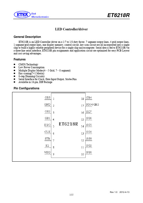
ET6218REtekMicroelectronics LED Controller/driverGeneral DescriptionET6218R is an LED Controller driver on a 1/7 to 1/8 duty factor. 7 segment output lines, 4 grid output lines, 1 segment/grid output lines, one display memory, control circuit, key scan circuit are all incorporated into a single chip to build a highly reliable peripheral device for a single chip microcomputer. Serial data is fed to ET6218R via a three-line serial interface, ET6218R pin assignments and application circuit are optimized for easy PCB Layout and cost saving advantages.Featuresz CMOS Technologyz Low Power Consumptionz Multiple Display Modes(4~5 Grid, 7~8 segment) z Key scaning(7×1 Matrix) z 8-step Dimming Circuitryz Serial Interface for Clock, Data Input/Output, Strobe Pins zAvailable in 18-pin, DIP PackagePin ConfigurationsPin DescriptionPin No.Pin NameI/ODescription5 DI/O(DIN&DOUT) I/OData I/O Pin(N-channel, Open-Drain)This pin outputs serial data at the falling edge of the shift clock andinputs serial data at the rising edge of the shift clock(starting from the lower bit)6 CLK I Clock Input PinThis pin reads serial data at the rising edge and outputs data at thefalling edge7 STB I Serial Interface Strobe PinThe data input after the STB has fallen is processed as a commandWhen this pin is “HIGH”, CLK is ignored 8 K1 I Key Data Input PinsThe data sent to these pins are latched at the end of the display cycle(Interface Pull-Low Resistor)2 GND ─ Ground Pin10~16 SG1/KS1~SG7/KS7 O Segment Output Pins(p-channel, open drain) Also acts as the Key Source 17 SG14/GR5 O Segment/Grid Output Pins 9 VDD ─ Power Supply 1,3,4,18 GR4~GR1 O Grid Output PinsINPUT/OUTPUT CONFIGURATIONSThe schematic diagrams of the input and output circuits of the logic section are shown below. 1. Input Pins :CLK ,STB&DIN(DI/O)2.Input Pins:K13.Output Pins:DOUT(DI/O),GR1~GR44.Output Pins:SG1~SG75.SG14/GR5Block DiagramFunctional DescriptionCOMMANDSA command is the first byte(b0~b7) inputted to ET6218R via the DI/O Pin after STB Pin has changed from HIGH to LOW State. If for some reason the STB Pin is set to HIGH while data or commands are being transmitted, the serial communication is initialized, and the data/commands being transmitted are considered invalid.Command 1:Display Mode Setting CommandsET6218R provides 2 display mode settings as shown in the diagram below:As started earlier a command isthe first one byte(b0~b7) transmitted to ET6218R via the DI/O Pin when STB is LOW. However, for these commands,the bit 3 to bit 6(b2~b5)are ignored,bit 7&bit 8(b6~b7) are given a value of 0.The Display Mode Setting Commands determine the number of segments and grids to be used (7 to 8 segments,4 to 5 grids). A display command ON must be excuted in order to resume display. If the same mode setting is selected, no command execution is take place, therefore, nothing happens. When Power is turned ON,the7-grid, 10-segment modes is selected.MSB LSB0 0 ──── b1 b0 b2~b5:Not RelevantDisplay Mode Setting:b1,b0—0 0:4 Grids,8 Segmentsb1,b0—0 1:5 Grids,7 SegmentsCommand 2:Data Setting CommandsData Setting Commands executes the Data Write or Data Read Modes for ET6218R. The data Setting Command, the bits 5 and 6(b4,b5) are ignored, bit 7(b6) is given the value of 1 while bit 8(b7) is given the valueof 0. Please refer to the diagram below. When Power is turned ON, bit 4 to bit 1(b3~b0) are given the value of 0.MSB LSB0 1 ──b3b2b1 b0 b4,b5:Not RelevantMode Setting: b3 —0:Normal OperationMode b3—1:Test ModeAddress Increment Mode Settings(Display Mode):b2—0:Increment Address after Data has been Writtenb2—1:Fixes AddressData Write&Read Mode Setting:b1,b0—0 0:Write Data to Display Modeb1,b0—1 0:Read Key DataET6218R KEY MATRIX&KEY INPUT DATA STORAGE RAMET6218R Key Matrix consists of 7×1 array as shown below:Each data entered by each key is stored as follows and read by a READ Command, starting from the lastCommand 3:Address Setting CommandsAddress Setting Commands are used to set the address of the display memory. The address is considered valid if it has a value of 00H to 0DH. If the address is set to 0EH or higher,the data is ignored until a valid addressis set. When power is turned ON,the address is set at 00H.MSB LSB1 1 ──b3b2b1 b0 b4,b5:Not RelevantThe address of b3~b0:00H~0DHDISPLAY MODE AND RAM ADDRESSData transmitted from an external device to ET6218R via the interface are stored in the Display RAM andare assigned address. The RAM addresses of ET6218R are given below in 8 bits unit.SG1…………SG4 SG5…………SG8 SG9…………SG12SG13…………SG1400H L 00H U 01H L 01H U DIG1 02H L 02H U 03H L 03H U DIG2 04H L 04H U 05H L 05H U DIG3 06H L 06H U 07H L 07H U DIG4 08H L 08H U 09H L 09H U DIG5 b0…………….b3 b4………………b7xxH L xxH ULower 4 bits Higher 4 bitsCommand 4:Display Control CommandsThe Display Control Commands are used to turn ON or OFF a display. It also used to set the pulse width.Please refer to the diagram below. When the power is turned ON,a 1/16 pulse width is selected and the displayedis turned OFF(the key scaning is stopped).MSB LSB1 0 ──b3b2b1 b0b4,b5 :Not RelevantDisplay Setting: b3—0:Display OFF(Key Scan Continues)b3—1:Display ONDimming Quantity Setting:000:Pulse width=1/16001:Pulse width =2/16010:Pulse width =4/16011:Pulse width =10/16100:Pulse width =11/16101:Pulse width =12/16110:Pulse width =13/16111:Pulse width =14/16SCANNING AND DISPLAY TIMINGThe Key Scanning and Display Timing diagram is given below. One cycle of key scanning consists of 2SERIAL COMMUNICATION FORMATThe following diagram shows the ET6218R serial communication format.The DI/O(DIN,DOUT) Pin is an N-channel,open-drain pin, therefore, it is highly recommended that an external pull-up resistor(1K~10K) must be connected to DI/O.waitIt must be noted that when the data is read, the waiting time(twait) between the rising of the eighth clock that has set the command and the galling of the first clock that has read the data is greater or equal to 1µs.SWITCHING CHARACTERISTIC WA VEFORMCLK STBt setup(Data Setup Time)≥100ns t hold(Data Hold Time)≥100nst CLK-STB(Clock-Strobe Time)≥1µs t THZ(Fall Time)≤10µst TZH(Rise Time)≤1µs t PZL(Propagation Delay Time)≤100ns fosc=Ocillation Frequency t PLZ(Propagation Delay Time)≤300ns t TZL<1µs t TLZ<10µsNote:Test condition undert THZ(Pull low risistor=10kΩ,Loading capacitor=300pf)t TLZ(Pull low risistor=10 kΩ,Loading capacitor =300pf)APPLICATIONCommand 2:Data Setting CommandCommand 3:Address Setting CommandData 1~n:Transfer Display Data(14 Bytes max) Command 4:Display Control CommandNote:1. Command 1:Display Mode Commands2. Command 2:Data Setting Commands3. Command 3:Address Setting Commands4. Command 4:Display Control CommnadsWhen IC power is applied for the first time, the contents of the Display RAM is not defined; thus, it is strongly suggested that the contents of the Display RAM must be cleared during the initial setting.Absolute Maximum Ratings(Ta = 25℃,GND = 0V)Parameter Symbol Ratings UnitSupply V oltage V DD-0.5~+7 VLogic Input V oltage V I-0.5~V DD+0.5 VDriver Output Current I OLGR +250 mA I OHSG -50 mAMaximum Driver Output Current/Total I TOTAL 400 mA Operating Temperature T opr-40~+85 ℃Storage Temperature T stg-55~+150 ℃Recommended Operating Range(Ta = -20~+70℃,GND = 0V)Parameter Symbol Min. Typ. Max. Unit Logic Supply V oltage V DD 3 5 5.5 V Dynamic Current(see Note)I DDdyn—— 5 mA High-Level Input V oltage V IH 0.6V DD—V DD VLow- Level Input V oltage V IL 0 —0.3V DD V Note:Test Condition:Set Display Control Commands=80H(Display Turn OFF State&under no load)Electrical Characteristics(V DD = 5V,GND = 0V,Ta = 25℃)Parameter Symbol Test Condition Min. Typ. Max.UnitHigh-Level Output Current I OHSG1V O =V DD-2V,SG1~SG7,SG14-20 -25 -40 mA I OHSG2V O =V DD-3V,SG1~SG7,SG14-25 -30 -50 mALow-Level Output Current I OLGR V O =0.3V,GR1~GR5, 100 140 —mA Low-Level Output Current I OLDOUT V O =0.4V 4 ——mASegment High-Level Output Current Tolerance I TOLSGV O =V DD-3V,SG1~SG7,SG14——+5 %High-Level Input V oltage V IH—0.6V DD— 5 VLow-Level Input V oltage V IL—0 —0.3V DDVOscillation Frequency fosc 350 500 650 kHz K1 Pull Down Resistor R KN V DD=5V 40—100 kΩ(V DD =3V , GND=0V , Ta=25℃)Parameter Symbol Test Condition Min. Typ. Max.Unit High-Level Output Current I OHSG1 V O = V DD -2V ,SG1~SG7,SG14-15 -20 -35 mALow-Level Output CurrentI OLGR V O =0.3V ,GR1~GR5, 100 140 — mA Low-Level Output Current I OLDOUT V O =0.4V 4 — — mASegment High-Level Output Current Tolerance I TOLSG V O = V DD -3V ,SG1~SG7,SG14— — +5% High-Level Input V oltage V IH — 0.8V DD—3.3 V Low-Level Input V oltage V IL — 0 — 0.3V DDVOscillation Frequency fosc 300 420 580 kHz K1 Pull Down ResistorR KN V DD =3V 40 —100 k Ω Application CircuitCOMMON CATHODE TYPE LED PANELNote :1. The capacitor(0.1µF)connected between the GND and VDD pins must be located as close as possible to the ET6218R chip.Package Dimension。
- 1、下载文档前请自行甄别文档内容的完整性,平台不提供额外的编辑、内容补充、找答案等附加服务。
- 2、"仅部分预览"的文档,不可在线预览部分如存在完整性等问题,可反馈申请退款(可完整预览的文档不适用该条件!)。
- 3、如文档侵犯您的权益,请联系客服反馈,我们会尽快为您处理(人工客服工作时间:9:00-18:30)。
ET6218REtekMicroelectronics LED Controller/driverGeneral DescriptionET6218R is an LED Controller driver on a 1/7 to 1/8 duty factor. 7 segment output lines, 4 grid output lines, 1 segment/grid output lines, one display memory, control circuit, key scan circuit are all incorporated into a single chip to build a highly reliable peripheral device for a single chip microcomputer. Serial data is fed to ET6218R via a three-line serial interface, ET6218R pin assignments and application circuit are optimized for easy PCB Layout and cost saving advantages.Featuresz CMOS Technologyz Low Power Consumptionz Multiple Display Modes(4~5 Grid, 7~8 segment) z Key scaning(7×1 Matrix) z 8-step Dimming Circuitryz Serial Interface for Clock, Data Input/Output, Strobe Pins zAvailable in 18-pin, DIP PackagePin ConfigurationsPin DescriptionPin No.Pin NameI/ODescription5 DI/O(DIN&DOUT) I/OData I/O Pin(N-channel, Open-Drain)This pin outputs serial data at the falling edge of the shift clock andinputs serial data at the rising edge of the shift clock(starting from the lower bit)6 CLK I Clock Input PinThis pin reads serial data at the rising edge and outputs data at thefalling edge7 STB I Serial Interface Strobe PinThe data input after the STB has fallen is processed as a commandWhen this pin is “HIGH”, CLK is ignored 8 K1 I Key Data Input PinsThe data sent to these pins are latched at the end of the display cycle(Interface Pull-Low Resistor)2 GND ─ Ground Pin10~16 SG1/KS1~SG7/KS7 O Segment Output Pins(p-channel, open drain) Also acts as the Key Source 17 SG14/GR5 O Segment/Grid Output Pins 9 VDD ─ Power Supply 1,3,4,18 GR4~GR1 O Grid Output PinsINPUT/OUTPUT CONFIGURATIONSThe schematic diagrams of the input and output circuits of the logic section are shown below. 1. Input Pins :CLK ,STB&DIN(DI/O)2.Input Pins:K13.Output Pins:DOUT(DI/O),GR1~GR44.Output Pins:SG1~SG75.SG14/GR5Block DiagramFunctional DescriptionCOMMANDSA command is the first byte(b0~b7) inputted to ET6218R via the DI/O Pin after STB Pin has changed from HIGH to LOW State. If for some reason the STB Pin is set to HIGH while data or commands are being transmitted, the serial communication is initialized, and the data/commands being transmitted are considered invalid.Command 1:Display Mode Setting CommandsET6218R provides 2 display mode settings as shown in the diagram below:As started earlier a command isthe first one byte(b0~b7) transmitted to ET6218R via the DI/O Pin when STB is LOW. However, for these commands,the bit 3 to bit 6(b2~b5)are ignored,bit 7&bit 8(b6~b7) are given a value of 0.The Display Mode Setting Commands determine the number of segments and grids to be used (7 to 8 segments,4 to 5 grids). A display command ON must be excuted in order to resume display. If the same mode setting is selected, no command execution is take place, therefore, nothing happens. When Power is turned ON,the7-grid, 10-segment modes is selected.MSB LSB0 0 ──── b1 b0 b2~b5:Not RelevantDisplay Mode Setting:b1,b0—0 0:4 Grids,8 Segmentsb1,b0—0 1:5 Grids,7 SegmentsCommand 2:Data Setting CommandsData Setting Commands executes the Data Write or Data Read Modes for ET6218R. The data Setting Command, the bits 5 and 6(b4,b5) are ignored, bit 7(b6) is given the value of 1 while bit 8(b7) is given the valueof 0. Please refer to the diagram below. When Power is turned ON, bit 4 to bit 1(b3~b0) are given the value of 0.MSB LSB0 1 ──b3b2b1 b0 b4,b5:Not RelevantMode Setting: b3 —0:Normal OperationMode b3—1:Test ModeAddress Increment Mode Settings(Display Mode):b2—0:Increment Address after Data has been Writtenb2—1:Fixes AddressData Write&Read Mode Setting:b1,b0—0 0:Write Data to Display Modeb1,b0—1 0:Read Key DataET6218R KEY MATRIX&KEY INPUT DATA STORAGE RAMET6218R Key Matrix consists of 7×1 array as shown below:Each data entered by each key is stored as follows and read by a READ Command, starting from the lastCommand 3:Address Setting CommandsAddress Setting Commands are used to set the address of the display memory. The address is considered valid if it has a value of 00H to 0DH. If the address is set to 0EH or higher,the data is ignored until a valid addressis set. When power is turned ON,the address is set at 00H.MSB LSB1 1 ──b3b2b1 b0 b4,b5:Not RelevantThe address of b3~b0:00H~0DHDISPLAY MODE AND RAM ADDRESSData transmitted from an external device to ET6218R via the interface are stored in the Display RAM andare assigned address. The RAM addresses of ET6218R are given below in 8 bits unit.SG1…………SG4 SG5…………SG8 SG9…………SG12SG13…………SG1400H L 00H U 01H L 01H U DIG1 02H L 02H U 03H L 03H U DIG2 04H L 04H U 05H L 05H U DIG3 06H L 06H U 07H L 07H U DIG4 08H L 08H U 09H L 09H U DIG5 b0…………….b3 b4………………b7xxH L xxH ULower 4 bits Higher 4 bitsCommand 4:Display Control CommandsThe Display Control Commands are used to turn ON or OFF a display. It also used to set the pulse width.Please refer to the diagram below. When the power is turned ON,a 1/16 pulse width is selected and the displayedis turned OFF(the key scaning is stopped).MSB LSB1 0 ──b3b2b1 b0b4,b5 :Not RelevantDisplay Setting: b3—0:Display OFF(Key Scan Continues)b3—1:Display ONDimming Quantity Setting:000:Pulse width=1/16001:Pulse width =2/16010:Pulse width =4/16011:Pulse width =10/16100:Pulse width =11/16101:Pulse width =12/16110:Pulse width =13/16111:Pulse width =14/16SCANNING AND DISPLAY TIMINGThe Key Scanning and Display Timing diagram is given below. One cycle of key scanning consists of 2SERIAL COMMUNICATION FORMATThe following diagram shows the ET6218R serial communication format.The DI/O(DIN,DOUT) Pin is an N-channel,open-drain pin, therefore, it is highly recommended that an external pull-up resistor(1K~10K) must be connected to DI/O.waitIt must be noted that when the data is read, the waiting time(twait) between the rising of the eighth clock that has set the command and the galling of the first clock that has read the data is greater or equal to 1µs.SWITCHING CHARACTERISTIC WA VEFORMCLK STBt setup(Data Setup Time)≥100ns t hold(Data Hold Time)≥100nst CLK-STB(Clock-Strobe Time)≥1µs t THZ(Fall Time)≤10µst TZH(Rise Time)≤1µs t PZL(Propagation Delay Time)≤100ns fosc=Ocillation Frequency t PLZ(Propagation Delay Time)≤300ns t TZL<1µs t TLZ<10µsNote:Test condition undert THZ(Pull low risistor=10kΩ,Loading capacitor=300pf)t TLZ(Pull low risistor=10 kΩ,Loading capacitor =300pf)APPLICATIONCommand 2:Data Setting CommandCommand 3:Address Setting CommandData 1~n:Transfer Display Data(14 Bytes max) Command 4:Display Control CommandNote:1. Command 1:Display Mode Commands2. Command 2:Data Setting Commands3. Command 3:Address Setting Commands4. Command 4:Display Control CommnadsWhen IC power is applied for the first time, the contents of the Display RAM is not defined; thus, it is strongly suggested that the contents of the Display RAM must be cleared during the initial setting.Absolute Maximum Ratings(Ta = 25℃,GND = 0V)Parameter Symbol Ratings UnitSupply V oltage V DD-0.5~+7 VLogic Input V oltage V I-0.5~V DD+0.5 VDriver Output Current I OLGR +250 mA I OHSG -50 mAMaximum Driver Output Current/Total I TOTAL 400 mA Operating Temperature T opr-40~+85 ℃Storage Temperature T stg-55~+150 ℃Recommended Operating Range(Ta = -20~+70℃,GND = 0V)Parameter Symbol Min. Typ. Max. Unit Logic Supply V oltage V DD 3 5 5.5 V Dynamic Current(see Note)I DDdyn—— 5 mA High-Level Input V oltage V IH 0.6V DD—V DD VLow- Level Input V oltage V IL 0 —0.3V DD V Note:Test Condition:Set Display Control Commands=80H(Display Turn OFF State&under no load)Electrical Characteristics(V DD = 5V,GND = 0V,Ta = 25℃)Parameter Symbol Test Condition Min. Typ. Max.UnitHigh-Level Output Current I OHSG1V O =V DD-2V,SG1~SG7,SG14-20 -25 -40 mA I OHSG2V O =V DD-3V,SG1~SG7,SG14-25 -30 -50 mALow-Level Output Current I OLGR V O =0.3V,GR1~GR5, 100 140 —mA Low-Level Output Current I OLDOUT V O =0.4V 4 ——mASegment High-Level Output Current Tolerance I TOLSGV O =V DD-3V,SG1~SG7,SG14——+5 %High-Level Input V oltage V IH—0.6V DD— 5 VLow-Level Input V oltage V IL—0 —0.3V DDVOscillation Frequency fosc 350 500 650 kHz K1 Pull Down Resistor R KN V DD=5V 40—100 kΩ(V DD =3V , GND=0V , Ta=25℃)Parameter Symbol Test Condition Min. Typ. Max.Unit High-Level Output Current I OHSG1 V O = V DD -2V ,SG1~SG7,SG14-15 -20 -35 mALow-Level Output CurrentI OLGR V O =0.3V ,GR1~GR5, 100 140 — mA Low-Level Output Current I OLDOUT V O =0.4V 4 — — mASegment High-Level Output Current Tolerance I TOLSG V O = V DD -3V ,SG1~SG7,SG14— — +5% High-Level Input V oltage V IH — 0.8V DD—3.3 V Low-Level Input V oltage V IL — 0 — 0.3V DDVOscillation Frequency fosc 300 420 580 kHz K1 Pull Down ResistorR KN V DD =3V 40 —100 k Ω Application CircuitCOMMON CATHODE TYPE LED PANELNote :1. The capacitor(0.1µF)connected between the GND and VDD pins must be located as close as possible to the ET6218R chip.Package Dimension。