模拟开关CH440芯片手册
S4000CH使用说明书_A110413_CHS
5.1 担保 ................................................................................................................................................ 16 5.2 运行原理.........................................................................................................................................16 5.3 技术参数.........................................................................................................................................16
co代表标定输出当co被激活并且标定完成模拟输出在5秒内从15ma上升到32ma停留在想要的4ma用户菜单结构故障运行设定标定值2590暂停重设进入气体核对模式进入标定模式argc新探头sel选择新探重设探头分钟探测到气体拿走气体重设探头寿命到100重设探头寿命到100通入气体然后自动拿走通入气体当完成后手动拿走禁止激励或非激励锁定或非锁定激励或非激励锁定或非锁定设定点lo预电器hi警继电器波特格式地址ch1modbus通道1ch2modbus通道1波特数据格式地址fi完成hm持续供磁am供磁rm拿走磁铁generalmonitormodels4000ch2101标定点设定为了调整s4000ch的标定点在仪表盖的wuxigmlogo上提供磁铁直到se显示出来
CH412 中文手册说明书

ESD 保护芯片CH412中文手册 版本:1B 1、概述CH412是四路ESD 保护二极管阵列,能够承受IEC 61000-4-2规定的最高±15KV 人体模型、±8KV 接触放电以及±15KV 气隙放电的ESD 脉冲,用于电子产品对外接口中的高速信号和差分信号以及通用信号的ESD 保护。
CH412K 提供4通道低电容二极管保护和TVS 瞬态电压抑制器箝位,适用于高速和中低速信号,可以用于USB 超速、高速和全速以及低速信号保护。
CH412Z 提供4通道TVS 瞬态电压抑制器箝位,适用于中低速信号,可以用于USB 全速和低速信号保护。
CH412K CH412Z2、特点● 支持±15KV 人体模型HBM 。
● 支持±8KV 接触放电。
● 支持±15KV 气隙放电。
● CH412K :内部4路独立箝位二极管,典型值1pF 的低输入电容,适用于高速和中低速信号。
● CH412Z :内部4路TVS 箝位保护,典型值20pF 的输入电容,适用于中低速信号。
● 采用SOT 小体积晶体管级贴片无铅封装,兼容RoHS 。
3、封装封装形式 塑体宽度 引脚间距 封装说明 订货型号 SOT363 1.25mm 49mil 0.65mm 26mil 小型6脚贴片 CH412K SOT353 1.25mm 49mil 0.65mm 26mil 小型5脚贴片 CH412Z 注:1、封装体积较小,正面印字仅有代号而不含全部型号,例如CH412Z 代号是12。
2、盘装,每盘整包装数量为3000只,可以零售,但是零售时不会逐个清点数量。
IO4 IO3 IO3 VCC IO44、型号CH412B已经停产,请换用CH412K,多出的两个通道可以悬空或并联(低速时)。
4、引脚CH412K 引脚号CH412Z引脚号引脚名称类型引脚说明2 2 GND 电源公共接地端,必须直接连接到全局地5 无VCC 电源正电源端,必须靠近引脚对GND连接0.1μF电容,用于USB信号保护时通常为3.3V(或者5V),用于其它信号须同被保护芯片的电源电压(2V~5V)1,3,4,6 1,3,4,5 IO1~IO4 信号ESD保护通道,与被保护芯片的信号引脚并联5、应用说明CH412设计用来与被保护芯片内置的ESD保护一起工作。
CH340 中文手册_图文
CH340 中文手册_图文USB 转串口芯片 CH3401、概述CH340 是一个 USB 总线的转接芯片,实现 USB 转串口、USB 转 IrDA 红外或者 USB 转打印口。
在串口方式下,CH340 提供常用的 MODEM 联络信号,用于为计算机扩展异步串口,或者将普通的串口设备直接升级到 USB 总线。
有关 USB 转打印口的说明请参考手册(二)CH340DS2。
在红外方式下,CH340 外加红外收发器即可构成 USB 红外线适配器,实现 SIR 红外线通讯。
异步串口 UART/RS232/IrDA 红外 SIR计算机 USB 或者 CH340其它转接芯片USB 主机转换并口打印机为 USB 打印机2、特点? 全速 USB 设备接口,兼容 USB V2.0,外围元器件只需要晶体和电容。
? 仿真标准串口,用于升级原串口外围设备,或者通过 USB 增加额外串口。
? 计算机端 Windows 操作系统下的串口应用程序完全兼容,无需修改。
? 硬件全双工串口,内置收发缓冲区,支持通讯波特率 50bps,2Mbps。
? 支持常用的 MODEM 联络信号 RTS、DTR、DCD、RI、DSR、CTS。
? 通过外加电平转换器件,提供 RS232、RS485、RS422 等接口。
? 支持 IrDA 规范 SIR 红外线通讯,支持波特率 2400bps 到 115200bps。
? 由于是通过 USB 转换的串口,所以只能做到应用层兼容,而无法绝对相同。
? 软件兼容 CH341,可以直接使用 CH341 的驱动程序。
? 支持 5V 电源电压和 3.3V 电源电压。
? 提供 SSOP-20 无铅封装,兼容 RoHS。
3、封装封装形式塑体宽度引脚间距封装说明订货型号 SSOP-20 5.30mm 209mil 0.65mm 25mil 超小型 20 脚贴片 CH340T SSOP-20 5.30mm 209mil 0.65mm 25mil 超小型 20 脚贴片 CH340R4、引脚引脚号引脚名称类型引脚说明 (括号中说明仅针对 CH340R 型号)19 VCC 电源正电源输入端,需要外接 0.1uF 电源退耦电容8 GND 电源公共接地端,直接连到 USB 总线的地线在 3.3V 电源电压时连接 VCC 输入外部电源, 5 V3 电源在 5V 电源电压时外接容量为 0.01uF 退耦电容9 XI 输入晶体振荡的输入端,需要外接晶体及振荡电容10 XO 输出晶体振荡的反相输出端,需要外接晶体及振荡电容6 UD+ USB 信号直接连到 USB 总线的 D+数据线7 UD- USB 信号直接连到 USB 总线的 D-数据线20 NOS# 输入禁止 USB 设备挂起,低电平有效,内置上拉电阻3 TXD 输出串行数据输出(CH340R 型号为反相输出)4 RXD 输入串行数据输入,内置可控的上拉和下拉电阻11 CTS# 输入 MODEM 联络输入信号,清除发送,低(高)有效12 DSR# 输入 MODEM 联络输入信号,数据装置就绪,低(高)有效13 RI# 输入 MODEM 联络输入信号,振铃指示,低(高)有效14 DCD# 输入 MODEM 联络输入信号,载波检测,低(高)有效15 DTR# 输出 MODEM 联络输出信号,数据终端就绪,低(高)有效16 RTS# 输出 MODEM 联络输出信号,请求发送,低(高)有效2 ACT# 输出 USB 配置完成状态输出,低电平有效18 R232 输入辅助 RS232 使能,高电平有效,内置下拉电阻NC. 空脚 CH340T:空脚,必须悬空17 CH340R:串口模式设定输入,内置上拉电阻, IR# 输入低电平为 SIR 红外线串口,高电平为普通串口CKO 输出 CH340T:时钟输出 1 NC. 空脚 CH340R:空脚,必须悬空5、功能说明CH340 芯片内置了 USB 上拉电阻,UD+和 UD-引脚应该直接连接到 USB 总线上。
Mini-Circuits USB-SP4T -63 单芯片4路交叉开关说明书
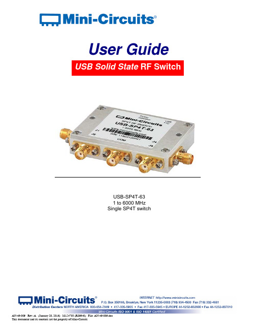
User Guide USB Solid State RF SwitchUSB-SP4T-631 to 6000 MHzSingle SP4T switchImportant NoticeThis guide is owned by Mini-Circuits and is protected by copyright, trademark and other intellectual property laws.The information in this guide is provided by Mini-Circuits as an accommodation to our customers and may be used only to promote and accompany the purchase of Mini-Circuits’ Parts. This guide may not be reproduced, modified, distributed, published, stored in an electronic database, or transmitted and the information contained herein may not be exploited in any form or by any means, electronic, mechanical recording or otherwise, without prior written permission from Mini-Circuits.This guide is subject to change, qualifications, variations, adjustments or modifications without notice and may contain errors, omissions, inaccuracies, mistakes or deficiencies. Mini-Circuits assumes no responsibility for, and will have no liability on account of, any of the foregoing. Accordingly, this guide should be used as a guideline only.TrademarksMicrosoft, Windows, Visual Basic, Visual C# and Visual C++ are registered trademarks of Microsoft Corporation. LabVIEW and CVI are registered trademarks of National Instruments Corporation. Delphi is a registered trademark of Delphi Technologies, Inc. MATLAB is a registered trademark of The MathWorks, Inc. Agilent VEE is a registered trademark of Agilent Technologies, Inc. Linux is a registered trademark of Linus Torvalds. Mac is a registered trademark of Apple Inc. Python is a registered trademark of Python Software Foundation Corporation.All other trademarks cited within this guide are the property of their respective owners. Neither Mini-Circuits nor the Mini-Circuits USB-SP4T-63 are affiliated with or endorsed or sponsored by the owners of the above referenced trademarks.Mini-Circuits and the Mini-Circuits logo are registered trademarks of Scientific Components Corporation.Mini-Circuits13 Neptune AvenueBrooklyn, NY 11235, USAPhone: +1-718-934-4500Email: **********************Web: Table of ContentsChapter 1 – General Information ......................................................... 4-6 1.1 Scope of the User Guide . (4)1.2 Warranty (4)1.3 Definitions (4)1.4 General safety precautions (4)1.5 Introduction (4)1.6 Service and Calibration (5)1.7 Contact Information (5)1.8 Technical description ....................................................................................... 5-61.8.1 Features of Mini-Circuits Switch Matrices (5)1.8.2 Intended Applications (5)1.8.3 Conformity (6)1.8.4 Supported Software environments (6)1.8.5 Included Accessories and Options (6)Chapter 2 – Installation and Setup .................................................... 7-10 2.1 Software Setup (7)2.2 Installation ........................................................................................................ 8-9 2.3 USB-SP4T-63 Physical Setup . (10)Chapter 3 – Using Mini-Circuits' .................................................... 11-16 3.1 USB interface ............................................................................................... 11-12 3.3 Sequence Mode ........................................................................................... 13-14 3.3 Firmware update .......................................................................................... 15-16 Chapter 4 – Revision history. (17)Chapter 1 – General Information1.1 Scope of the User GuideThis user guide provides general introduction, installation instructions and operating information for Mini-Circuits USB solid state switches.1.2 WarrantySee Mini-Circuits website /support/ordering.html for warranty information.1.3 DefinitionsNote: A note advises on important information you may need to ensure proper operation of the equipment.There is no risk to either the equipment or the user.A caution advises about a condition or procedure which can cause damage to theequipment (no danger to users).A warning alerts to a possible risk to the user and steps to avoid it. DO NOT proceeduntil you are sure you understand the warning.1.4 General safety precautionsPlease observe the following safety precautions at all times when using Mini-Circuits USB RF switch matrices.Ensure that all instruments using mains power supply are properly grounded to prevent risk of electrical shock.1. Do not attempt to switch signals of greater power than the switch is rated for in its datasheet.2. Safe power input degrades below specified frequency range. Do not input signals below the specified frequency range.1.5 IntroductionMini-Circuits has developed a new solid state USB RF switch. The USB-SP4T-63 is a compact case (2.25" x 1.50" x 0.475") with all power drawn from USB and no moving parts. The switch operates from 1 to 6000 MHz; with high isolation (50 dB typ). The switch is a USB HID devices and is “plug & play,” with no driver installation needed. The USB-SP4T-63 can be controlled via the supplied GUI, or most common lab test software using supplied DLLs. Mini-Circuits even provides the command codes for direct control (See programming guide for details)CAUTIONWARNINGWARNINGCAUTION1.6 Service and CalibrationThe USB-SP4T-63 does not require any periodic service or calibration. The only user service possible for the switch is external cleaning of the case and connectors as needed. Do not use any detergents or spray cleaning solutions to clean the switch. To clean the connectors use an alcohol solution, and to clean the case a soft, damp cloth.1.7 Contact InformationMini-Circuits inc.13 Neptune AveBrooklyn, NY 11235Phone: 1-718-934-4500General Fax: 1-718-332-4661Sales / Customer Service Fax: 1-718-934-7092**********************For regional offices and tech support see /contact/offices.html1.8 Technical description1.8.1 Features of Mini-Circuits Switch Matrices• 1 to 6000 MHz; absorptive solid state switch• Electronic switching; Isolation 50 dB typ.• High power handling, 1W• All RF ports SMA(F)• Programmable, timed switching sequence as fast as 5µsec between transitions• Easy GUI installation and operation, simplifies complex switching and timing setups• USB HID ”plug & play” device• ActiveX com object and .Net class library for use with other software: C++, C#, CVI®, Delphi®, LabVIEW® 8 or newer, MATLAB® 7 or newer, Python, Agilent VEE®, Visual Basic®, Visual Studio® 6 or newer, and more(see programming handbook and application note AN-49-001 for details)• User friendly Graphical User Interface for any Windows® 32 or 64 bit computer command line support for Linux® computers• All power via USBFor Additional details, performance data and graphs, outline drawing, ordering information and environmental specifications, see our catalog at:/products/usb_rfspdt_switches.shtml1.8.2 Intended ApplicationsMini-Circuits USB-SP4T-63 switches are intended for indoor use in:- Lab and test equipment setups for both manual and automated measurements- Control systems- Automated switching of signal paths in a complex systemThe models can be used by anyone familiar with the basics of electronics measurements or electronic control systems.1.8.3 ConformityMini-Circuits USB-SP4T-63 switches conform to all requirements for the following international standards:RoHS – The model compl ies with EU directive for Restriction of Hazardous Substances for 6 substances.USB 2.0 – The model meets the specifications of the Universal Serial Bus Ver. 2.0 communication standard as described by USB-IF.USB HID – The model meets the requirements for Universal Serial Bus HumanInterface Devices according to USB-IF’s Device Class Definition for HumanInterface Devices firmware rev. 1.11.1.8.4 Supported Software environmentsMini-Circuits USB-SP4T-63 switches have been tested in the following operating systems:32 bit systems: Windows 8, Windows 7, Windows Vista, Windows XP Windows 9864 bit systems: Windows 8, Windows 7, Windows Vista, LinuxThe switches will work with almost any software environment that supports ActiveX or .Net including: C++, C#, CVI®, Delphi®, LabVIEW® 8 or newer, MATLAB® 7 or newer, Python, Agilent VEE®, Visual Basic®, AutoIT, Visual Studio® 6 or newer, and moreFor more information see the Synthesized Signal Generator Programming Manual and application note AN-49-001 on our website.1.8.5 Included Accessories and OptionsThe USB-SP4T-63 is supplied with a 2.6 ft' USB cable and a software CD. For additional details and ordering information, go to/MCLStore/ModelSearch?search_type=info&model=USB-SP4T-63 .Chapter 2 – Installation and SetupSystem requirements for the switch are a computer (Pentium II or better) with support for USB HID. To run the GUI program a Windows operating system for either 32 or 64 bits is also required.2.1 Software SetupIf you have had any problems installing the software, we’re here to help.Try following these complete step-by-step instructions. If you still experience problems, give us a call at Mini-Circuits Worldwide Technical support. It’s (718) 934-4500 or e-mail ************************************,/contact/worldwide_ tech_support.html for other regional numbers and addresses.2.1.1 First save all work in progress and close any other programs that may be running. 2.1.2 Next,Insert the Mini-Circuits CD into the CD-ROM drive, or download the full CD software from . If installing from files downloaded from the web - unzip the downloaded files to a temporary folder on your desktop or C: drive, then open the file folder you created and double-click the “Install” icon.2.1.3 If installation from the CD does not start automatically, run install.exe from the <CD drive> root directory.Figure 2.1.3 CD file listing window2.2 Installation2.2.1 The installer window should now appear. Click the “Install Now” button.Figure 2.2.1 Installation window2.2.2 The license agreement should now appear. To proceed, click “I Agree” andthe “Continue” button.Figure 2.2.2 License agreement2.2.3 The installation program will launch . Click the “OK” button to continue.Figure 2.2.3 Installation Program windowFigure 2.2.6: Installation complete2.2.4 The destination directory window will appear. At this point it’s a good idea totake a second and confirm the full destination address for the software. In most cases, the default will be your computer’s hard drive (C:)\Program Files\Mini-Circuits RF Switch Box\. Or Change it then click the large button at the top to continue.Figure 2.2.4: Destination Directory window2.2.5 The Program Group window will appear. This window allows you to select the program group under which the link for the switch controller program in the Start Menu will be created. If you change the Program Group for this software, be sure to record that information together with your destination address. Click on “Continue” to proceed.Figure 2.2.5: Program Group Window2.2.6 In a second or two, your installation will be complete. Click “OK” toclose the installer.2.3 USB-SP4T-63 Physical SetupConnect the USB-SP4T-63 to the computer using the provided MUSB-CBL-3+ USB cable orequivalent, then connect the required RF connections.Note the maximum rating power input in the datasheet and the conditions specified for CAUTIONit. Exceeding these values may damage the switch.Chapter 3 – Using Mini-Circuits' USB-SP4T-633.1 USB interfaceMini-Circuits' Solid State Switch controller GUI allows you to set manually the switch state or runa timed sequence of any configuration you can imagine.3.1.1 Go to the Start menu and select All Programs>Mini-Circuits Solid State Switch(default), or go to the other destination address you selected earlier. The “Mini-Circuits Solid State Switch” icon should be waiting there for you. Click on it and get started!3.1.2 If multiple switches are connected to the computer, the initial screen willshow a list of S/N for connected units. Select the unit you wish to start with and click OK, or click Cancel to exit the program. The program can handle up to 24 units connectedsimultaneously.Figure 3.1.2: Unit selection screen3.1.3 If no switch matrices are connected to the computer via USB, or there is aproblem with the power or USB connection of the unit an alert will pop up. Click OK, then check the power and USB connections of the unit before trying again.Figure 3.1.3: No USB Unit found3.1.4 Once the GUI is started you can:•Click on the switch setting you wish to use•Use the Sequence mode to set a timed switching sequence (see section 3.2 )•Select the (fw) indicator to upgrade the firmware (See section 3.3)•Update the unit address by entering an integer in the 1-255 range in the Address field below the S/N and clicking Set.Figure 3.1.4 Main screen3.2 Sequence ModeUSB-SP4T-63 supports a “Sequence Mode” which allows the user to program a timedsequence of switch states. This sequence can either be controlled from the computer or loaded into the switch’s internal microcontroller, allowing very fast switching sequences to be triggered with no further USB communication. The sequence mode is available with Firmware Rev. A3 or greater. See section 3.3 for details on upgrading firmware.3.2.1 After clicking on the Sequence mode button, the User sequence window will open. The user sequence can be used in two modes•PC control where each command is sent individually with timing controlled by the computer. Minimum dwell time in PC control is 5 msec and the GUI will show an indicator of the current state and number of cycles run.• High speed mode where the entire sequence is sent to the device and timing is controlled by the switch’s internal micro-controller. Minimum dwell time in high speed mode is 5 µsec, however no external indication of the switch state is available whilethe sequence is running and any command sent to the switch will cause it to stop the sequence.Figure 3.2.1 Main screen1 2 3 4 5 6 7 8 9 103.2.2 The user sequence controls are:#Name Description 1Icons Allow clearing a current sequence, opening a previously saved sequence or saving the current sequence. 2Step Listing of the step number in the sequence. Up to 100 steps in a sequenceare possible. 3Com => The port to which the Com port connects in any given step 4Dwell Time The time the switch will hold at each step. 5Time units The time units of the dwell time set in each step. The time units can be set independently for each step to seconds, milliseconds or microseconds(available only in high speed mode) 6Control mode Select PC control or high speed mode 7Direction Select direction the sequence will run. Forward is the sequence as shown, reverse will run the sequence from last step to first and bi-directional will run the sequence from first step to last, then from last step to first. 8Cycles Number of cycles to run, can be set from 1 to 65535. If “run continuously” is selected the sequence will keep repeating until stopped. 9Run Start running the sequence with the current settings. 10Stop Stop the switch in the current setting3.2.3 To insert a new step into the middle of a sequence click on the step numberfollowing the desired location and press ‘Insert’. To delete a line click on the relevant step number and press ‘delete’.3.2.4 Regardless of the dwell time set, or which mode the GUI is in switching timewill remain the same.Figure 3.2.4 Switching time with dwell time=5µsec1.8µsec RF Out (J1) RF Out (J2)3.3 Firmware update3.3.1 All USB-SP4T-63 units are shipped with the latest available firmware and an update is usually not required. Mini-Circuits occasionally makes firmware update files available as a courtesy to add additional features or correct known issues. Please contact ******************************for details.3.3.2 Once the switch controller GUI i s installed and started (see chapter 2) you will note an (fw) indicator in the upper right corner of the main screen.Figure 3.3.2 Firmware indicator on main screen3.3.3 In order to update your switch firmware, you must have a switch a Windows computer with Mini-Circuits’ Switch Controller software installed.A power interrupt, to either the computer or the switch while the firmware is being updated may cause the firmware to be corrupted. It is therefore recommended to onlyupdate the firmware while both the switch and the computer are connected to an Uninterruptable Power Supply (UPS).3.3.4 Click on the ‘(fw)’ indicator, this will cause the firmware - info window to open (See Fig. 3.3.4). The ‘Firmware’ listed is the version of the firmware installed in your switch matrix. Click on “Update Firmware” to select a new firmware version to install or click ‘Exit’ to close the firmware – info window.Figure 3.3.4: Firmware Information WindowCAUTION3.3.5 A browse window will open to the firmware directory under the path you selected when installing the GUI program (See Fig. 3.3.5). Navigate to where you saved your firmware file, Select the firmware version you wish to install and click ‘O.K’.Figure 3.3.5: Firmware - Browse Window3.3.6 The selected file will be installed in the switch the process will take up to a minute.Figure 3.3.6: Firmware - Progress Bar Window3.3.7 After the firmware has updated an alert will appear. Click ‘OK’ to shut down the Switch Controller program and then restart it normally.Figure 3.3.7: Firmware - Successful UpdateChapter 4 – Revision historyJune 25, 2015: Created user guide Rev OR.January 20, 2016: Updated firmware upgrade section; Added description of new switching sequence function. Rev A。
Alarmtech VMC 440 磁感应门窗传感器说明书

VMC 440 Instruction Manual 4-VMC440-01© 2015 Alarmtech Rev. VMC440 1511en Page 1 of 2Magnetic ContactDESCRIPTIONMC 440 is a magnetic contact with opening contact for surface mount. It can be used in security system and industrial control systems for protection of doors and windows against unauthorized opening. It is easy to mount and has screw terminals with wire guards. It is available with build in resistors of any value and configuration on customer request. With enclosed plastic distances and separate accessories like Z-bracket and L-bracket it is possible to mount the contact on steel.CIRCUIT DIAGRAM (SHOWN WITHOUT MAGNET FIELD)Fig 1.MC 440 with configuration for separate sabotage loop:Fig.2. MC 440 with one resistor Rp parallel over reed mounted in the terminals with many contacts in a loop:Fig 3. MC 440 with two resistor mounted in the terminals for a end of line contact when only one contact used in the loop:Fig. 4. MC 440-PRpSRs with build in resistors:A = End Of Line using 2 resistors.B = using only the Rp resistor to mount more contacts on one loop.TECHNICAL DATASwitching voltage max. 48 V DC/ACSwitching current max. 400 mA DC/peak AC Contact rating max.10 WVMC 440 Instruction Manual4-VMC440-01© 2015 AlarmtechRev. VMC440 1511enPage 2 of 2OPERATING PRINCIPLEMC 440 magnetic contact has two parts: the contact part with a reed switch and the magnet part. In its neutral position the reed switch remains closed under the force of the magnetic field. Opening the monitored object increases the distance between the reed switch and the magnet. This reduces the influence of the magnetic field on the reed switch until it opens and activates an alarm.Magnetic contacts should not be installed in the vicinity of strong magnetic fields.INSTALLATIONContact and magnet should be installed in parallel, above or besides each other corresponding to each other. Offset will reduce the working distances. The contact should be mounted on the stationary part of the monitored object (ex. door frame) and the magnet on the movable part (ex. door leaf).For sites where it is impossible to mount the contact directly, spacers and aluminium brackets are available. Spacers enable installation of the contact on ferromagnetic surfaces. Brackets can be used to mount the contact parts away from a ferromagnetic surface or to solve problems with aligning the contact with the magnet. Contact and/or magnet should be screwed to the oval slots in the brackets and adjusted to a suitable position.Only non-ferromagnetic screws may be used for mounting the contact.After the installation, use an ohmmeter to check the electrical connections and test the operation of the magnetic contact.Warning: applying excessive force to the housing of the contact may damage the glass body of the reed switches inside.Warning: appropriate accessories must be used for installation in ferromagnetic environment.ORDER INFORMATIONMC 440 is standard available with build in resistors 1% tolerance of any chosen value.For model MC 400 the resistors can be self-mounted to the terminals of the product of any chosen value by installer. MC 440 is universal and can be used with one resistor parallel to the alarm switch mounted on terminal 1 and 2 and with two resistors one in parallel mounted on terminal 1 and 2 and one in series to the reed mounted on terminal 3 and 4.MC 400-PRpSRs is the universal contact with build in resistor. It is universal for one and two resistor by connecting the the loop either A to terminal 1and 2 for a parallell resistor to reed or B connected to terminal 1 and 3 for two resistors Rp and Rs. We keep stock of some units with build in standard resistor values. If in this case the two resistors have different value use S in front of the value in series and P for parallel to the reed contact when ordering. Any resistance values with tolerance 1% can be ordered with min. quantity of 100pcs.For special orders of build in resistors use the following ordering information MC 440-PRpSRs∙ Parallel to reed use prefix P and resistor value ∙ In series to reed use prefix S and resistor value ∙With the same value of Rp and Rs use MC 440-2xRORDER INFORMATIONUniversal contact with 2 resistors build in as we keep in stock. The design allows installer to use one or both.AccessoriesWe reserve the right to changes without notice.。
PCIE扩展ROM控制芯片CH366硬盘和网络安全隔离卡方案
PCIE扩展ROM控制芯片CH366硬盘和网络安全隔离卡方案版本: 11、概述安全隔离卡用于将普通计算机分为安全环境(内网)和开放环境(外网),内网和外网使用不同的硬盘并且连接到不同的网络,从而能够避免硬盘中的重要数据通过网络等方式泄露。
一般的双网卡方案、多重引导卡或者多用户管理卡只是在逻辑层提供硬盘数据隔离,而硬盘和网络安全隔离卡的特点主要是在物理层提供硬盘数据隔离,确保更高的数据安全性。
现有的技术方案主要是单网卡、双硬盘物理切换隔离,通常都需要在启动时选择内网或者外网,这些选择界面和切换操作通常由扩展ROM中的启动程序完成。
2、用户的功能需求分析①用户需要在开机后选择将使用内网的安全环境,还是外网的开放环境,所以安全隔离卡应该能够在开机时向用户提供选择界面,而且应该是在DOS或者Windows等操作系统引导之前。
②当用户选择完后,安全隔离卡需要执行内外网的环境切换,也就是说,需要在选择界面(软件)与隔离卡切换电路(硬件)之间建立通讯。
③当启动时切换选择后,必须确保不能在Windows等系统的运行过程中被黑客无意或者恶意的切换,否则将导致硬盘数据不完整以及数据通过外网泄露,所以安全隔离卡需要一个切换锁定装置。
当隔离卡在启动时切换完成后,必须锁定防止再被切换,直到关机或者重启才能解除。
④美观需求。
早期产品是从计算机后壳引出电线接一个电器开关到桌面,由用户随时拨动开关,所以就很难做到美观,也不完全,容易无意中碰到,完全不象一个高科技的IT产品。
⑤方便性和智能化,体现在软件功能上。
新式的隔离卡通常采用扩展ROM程序,根据用户的使用习惯提供仿Windows中文界面和智能提示,以及个性化的启动图片。
⑥方案的统一性和可升级性。
同一方案既能支持PATA并口硬盘,也能支持SATA串口硬盘,便于批量采购和备货,便于简化售后服务。
⑦软硬件的兼容性,由所采用的技术方案而定。
例如,IDE接口只用于硬盘和光驱产品,当前的UDMA133硬盘工作在133MHz高频上,如果通过拦截硬盘IDE接口获取扩展ROM发出的切换指令,那么就会增加IDE接口的负载,对于更高速度的SATA接口则问题更严重,很容易产生主板兼容性问题,或者影响硬盘数据的传输速度,好的技术方案应该尽量采用成熟的标准化技术,例如通过PCI-Express总线的I/O端口获取扩展ROM发出的切换指令。
基于PROTEUS的输、受血一体的血型匹配指示电路设计

基于PROTEUS的输、受血一体的血型匹配指示电路设计作者:周灵彬来源:《数字技术与应用》2017年第11期摘要:现有的血型匹配电路或功能单一,只具有输血匹配或受血匹配指示功能;或关注器件应用的技术性而忽略了实用性。
故设计一种直观、方便操作的输、受血匹配指示电路。
主要由数字门电路、模拟开关组成,并通过一按键来切换输、受血状态。
本电路在PROTEUS仿真软件中测试成功。
关键词:血型匹配;门电路;模拟开关;仿真中图分类号:TN79 文献标识码:A 文章编号:1007-9416(2017)11-0181-03人类基本血型有四种:A、B、AB和O型。
输血时输血者的血型与受血者的血型不是简单的可逆关系,而必须符合一定的授受关系,如图1所示。
即:(1)O型血可输给任意血型的人,但O型血的人只能接受O型血;(2)AB型血只能输给AB型的人,但AB血型的人能接受所有血型;(3)A型可输给A型与AB血型的人,但只接受A型血与O型血;(4)B 型血可输给B型与AB血型的人,但只接受B型血与O型血。
1 由数据选择器等搭建的血型匹配电路[1-2]现有的血型匹配电路或只实现了单一的输血或是受血指示功能;或是注重元件应用而实现的匹配电路,常见的设计思路如下:4种血型可以用两个逻辑变量组合表示,假设00代表A 型、01代表B型、10代表AB型、11代表O型。
那么输血与受血就需要两组两位逻辑变量,是否匹配成功可用一位逻辑变量表示。
如此得到如表1的真值表。
在要求用八选一数据选择器(74151)等来实现时,由真值表得到表2所示的卡诺图,因此逻辑式可以表示为:Y=m0D'+m1D'+ m2D+m3D'+m5D’十m6+m7故:D0=D1=D3=D5=D',D2=D,D4=0,D6=D7=1。
根据74151的功能表,如图2所示,结合上式,可设计出如图3所示的血型匹配指示电路。
要判断血型是否匹配,必须要将表1和图3结合起来看。
低阻宽带模拟芯片

引脚说明 正电源
公共接地,数字信号参考地 全局使能输入,低电平有效 单刀四掷模拟开关选择输入: 00 选择 1#端(S1x);01 选择 2#端(S2x); 10 选择 3#端(S3x);11 选择 4#端(S4x) 单刀四掷模拟开关的公共端
单刀四掷模拟开关的 1#端,IN1&IN0 引脚输入 00 选中
4.2. CH444 引脚
引脚号 16 8 1
引脚名称 VCC GND EN#
2、14
IN1、IN0
7、9 6、10 5、11 4、12 3、13
15
YA、YB S1A、S1B S2A、S2B S3A、S3B S4A、S4B
NC.
类型 电源 电源 输入
输入
模拟信号 输入输出 模拟信号 输入输出 模拟信号 输入输出 模拟信号 输入输出 模拟信号 输入输出
CH440 手册、CH444 手册、CH441 手册
1
4 单刀双掷低阻模拟开关芯片 CH440
2 单刀四掷低阻模拟开关芯片 CH444
4 单刀单掷低阻模拟开关芯片 CH441
手册 版本:1A
1、概述
CH440 是 4 通道低阻宽带双向模拟开关芯片。CH440 包含 4 通道单刀双掷模拟开关,高带宽,低 导通电阻,可以用于视频或者 USB 信号二选一切换。
CH440 手册、CH444 手册、CH441 手册
3
4、7、9、12 2、5、11、14 3、6、10、13
DA、DB、 DC、DD
S1A、S1B、 S1C、S1D S2A、S2B、 S2C、S2D
模拟信号 输入输出 模拟信号 输入输出 模拟信号 输入输出
单刀双掷模拟开关的公共端 单刀双掷模拟开关的 1#端,IN 引脚输入低电平选中 单刀双掷模拟开关的 2#端,IN 引脚输入高电平选中
- 1、下载文档前请自行甄别文档内容的完整性,平台不提供额外的编辑、内容补充、找答案等附加服务。
- 2、"仅部分预览"的文档,不可在线预览部分如存在完整性等问题,可反馈申请退款(可完整预览的文档不适用该条件!)。
- 3、如文档侵犯您的权益,请联系客服反馈,我们会尽快为您处理(人工客服工作时间:9:00-18:30)。
4、引脚
4.1. CH440G、CH440R、CH445P 引脚
CH440 引脚 CH445P 引脚 引脚名称 类型
引脚说明
16
14
VCC
电源
正电源
8
6、0
GND
电源
公共接地,数字信号参考地
15
13
EN#
输入
全局使能输入,低电平有效
1
15
IN
输入
单刀双掷模拟开关选择输入: 高电平选择 2#端(S2x);低电平选择 1#端(S1x)
最小值 2.1
-0.5 1.8
0 -0.3
典型值 3.3 0.1 0.6
0.1 ±0.005
7 9 28 14
最大值 3.9 5 3 0.7
VCC+0.5 5
±0.5 1.5
VCC+0.3 9 13 38 20
单位
V uA mA V V uA uA V V Ω Ω Ω Ω
6.4. 5V 开关芯片模拟开关时序参数(测试条件:TA=25℃,VCC=5V,VANA=0V)
DC S2C
Decode & Drive
EN#
IN
CH443K 是单通道低阻宽带双向模拟开关芯片。CH443K 包含 1 通道 SPDT 单刀双掷模拟开关,高
CH440、CH442、CH443、CH444、CH445 手册
2
带宽,低导通电阻,可以用于视频或者 USB 信号二选一切换。
CH0 COM
单刀四掷模拟开关的 1#端,IN1&IN0 引脚输入 00 选中
单刀四掷模拟开关的 2#端,IN1&IN0 引脚输入 01 选中
单刀四掷模拟开关的 3#端,IN1&IN0 引脚输入 10 选中
单刀四掷模拟开关的 4#端,IN1&IN0 引脚输入 11 选中 保留引脚,禁止连接
5、功能说明
CH440G、CH440R 和 CH445P 内部的 4 通道单刀双掷模拟开关,由 EN#引脚控制实现统一使能,由 IN 引脚选择进行统一切换。下表是其控制真值表。
CH440、CH442、CH443、CH444、CH445 手册
1
4 单刀双掷 5V 低阻模拟开关芯片 CH440G/R
2 单刀双掷 5V 低阻模拟开关芯片 CH442E
1 单刀双掷 5V 低阻模拟开关芯片 CH443K
2 单刀四掷 5V 低阻模拟开关芯片 CH444G/R
4 单刀双掷 3.3V 低阻模拟开关芯片 CH445P
1
X
X 全部断开 全部断开
6、参数
6.1. 绝对最大值(临界或者超过绝对最大值将可能导致芯片工作不正常甚至损坏)
名称 TA TS VCC VCC VIO Isw Iall
参数说明 工作时的环境温度 储存时的环境温度 5V 开关芯片的电源电压(VCC 接电源,GND 接地) 3.3V 开关芯片的电源电压(VCC 接电源,GND 接地) 数字或者模拟输入或者输出引脚上的电压 模拟开关的连续通过电流 所有模拟开关的连续通过电流的总和
SC70-6L SOT363
1.25mm
49mil
0.65mm
26mil
缩小型 6 脚贴片
CH443K
SOP-16
3.9mm 150mil 1.27mm 50mil 标准的 16 脚贴片
CH444G
TSSOP-16 4.4mm 173mil 0.65mm 25mil 薄小型的 16 脚贴片 CH444R
IOFF3
模拟开关在关闭状态下的泄漏电流
VANA3
推荐的模拟信号的电压范围
VANAX3
允许的模拟信号的电压范围
RON1 模拟开关导通电阻,模拟信号电压为 0.8V
RON2 模拟开关导通电阻,模拟信号电压为 1.2V
RON3 模拟开关导通电阻,模拟信号电压为 2.0V
RON4 模拟开关导通电阻,模拟信号电压为 3.3V
单刀双掷模拟开关的 CH1 端, SEL 引脚输入高电平选中
4.4. CH444G、CH444R 引脚
引脚号 16 8 1
2、14
7、9
6、10
5、11
4、12
3、13 15
引脚名称 VCC GND EN#
IN1、IN0
YA、YB
S1A、S1B
S2A、S2B
S3A、S3B
S4A、S4B NC.
类型 电源 电源 输入
参数说明 电源电压 静态电源电流,所有数字引脚接 VCC 或 GND 静态电源电流,所有数字引脚 3.4V 数字引脚低电平输入电压 数字引脚高电平输入电压 数字引脚的输入泄漏电流 模拟开关在关闭状态下的泄漏电流 推荐的模拟信号的电压范围 允许的模拟信号的电压范围 模拟开关导通电阻,模拟信号电压为 1V 模拟开关导通电阻,模拟信号电压为 2V 模拟开关导通电阻,模拟信号电压为 3.4V 模拟开关导通电阻,模拟信号电压为 5V
名称 CIN COFF CON BW TON TOFF
参数说明
数字输入引脚电容,F=1MHz 开关关闭时模拟信号引脚电容,F=1MHz 开关导通时模拟信号引脚电容,F=1MHz 模拟开关 3DB 信号带宽(非担保参数) 模拟开关开启延时,RL=75Ω,CL=20pF 模拟开关关闭延时,RL=75Ω,CL=20pF
订货型号
SOP-16
3.9mm 150mil 1.27mm 50mil 标准的 16 脚贴片
CH440G
TSSOP-16 4.4mm 173mil 0.65mm 25mil 薄小型的 16 脚贴片 CH440R
MSOP-10 3.0mm 118mil 0.50mm 19.7mil 微小型的 10 脚贴片 CH442E
(S1B) CH1
(S2B)
类型 电源 电源
输入
模拟信号 输入输出 模拟信号 输入输出 模拟信号 输入输出
4
引脚说明 正电源 公共接地,数字信号参考地 单刀双掷模拟开关选择输入: 高电平选择 CH1 端;低电平选择 CH0 端
单刀双掷模拟开关的公共端
单刀双掷模拟开关的 CH0 端, SEL 引脚输入低电平选中
10、13
8、11 S2C、S2D 输入输出
IN 引脚输入高电平选中
4.2. CH442E 引脚
引脚号 10 5 9
引脚名称 VCC GND EN#
1
IN
4、6
DB、DC
2、8
S1B、S1C
3、7
S2B、S2C
类型 电源 电源 输入
输入
模拟信号 输入输出 模拟信号 输入输出 模拟信号 输入输出
引脚说明 正电源 公共接地,数字信号参考地 全局使能输入,低电平有效 单刀双掷模拟开关选择输入: 高电平选择 2#端(S2x);低电平选择 1#端(S1x)
开关芯片支持额定 3.3V 电源电压,低至 1.8V 电源可用。 ● 提供 SOP-16、TSSOP-16、QFN16、MSOP-10 和 SC70-6L(SOT-363)等封装形式,兼容 RoHS。
3、封装
CH440、CH442、CH443、CH444、CH445 手册
3
封装形式
宽度
引脚间距
封装说明
QFN16
3*3mm
0.50mm 19.7mil 方形无引线 16 脚
CH445P
注:1、原型号 CH440E 已用新型号 CH442E 代替,引脚和功能完全相同。
2、CH443K 为盘装,每盘整包装数量为 3000 只,可以零售,但是零售时不会逐个清点数量。
3、CH443K 封装体积较小,正面印字仅有代号 43 而不含全部型号。
输入
模拟信号 输入输出 模拟信号 输入输出 模拟信号 输入输出 模拟信号 输入输出 模拟信号 输入输出
空脚
引脚说明 正电源 公共接地,数字信号参考地 全局使能输入,低电平有效 单刀四掷模拟开关选择输入: 00 选择 1#端(S1x);01 选择 2#端(S2x); 10 选择 3#端(S3x);11 选择 4#端(S4x) 单刀四掷模拟开关的公共端
EN#
IN
DB
DC
0
0选择 S2C
1
X 全部断开 全部断开
CH440、CH442、CH443、CH444、CH445 手册
5
CH443K 内部的单通道单刀双掷模拟开关,由 SEL 引脚选择进行切换。下表是其控制真值表。
SEL
COM
0 选择 CH0 1 选择 CH1
4、7、 9、12
2、5、 DA、DB、 模拟信号
7、10
DC、DD 输入输出
单刀双掷模拟开关的公共端
2、5、 16、3、 S1A、S1B、 模拟信号
单刀双掷模拟开关的 1#端,
11、14
9、12 S1C、S1D 输入输出
IN 引脚输入低电平选中
3、6、 1、4、 S2A、S2B、 模拟信号
单刀双掷模拟开关的 2#端,
EN#
IN
DA
DB
DC
DD
0
0 选择 S1A 选择 S1B 选择 S1C 选择 S1D
0
1 选择 S2A 选择 S2B 选择 S2C 选择 S2D
1
X 全部断开 全部断开 全部断开 全部断开
CH442E 内部的双通道单刀双掷模拟开关,由 EN#引脚控制实现统一使能,由 IN 引脚选择进行统 一切换。下表是其控制真值表。
最小值 -40 -55 -0.5 -0.5 -0.5 0 0
最大值 85 125 6.5 4.4
VCC+0.5 30 120
单位 ℃ ℃ V V V mA mA
6.2. 5V 开关芯片电气参数(测试条件:TA=25℃,VCC=5V)