(完整版)TMS320C6455高速SRIO接口设计
TMS320C6455 硬件设计 PCB Layout

1Prerequisites PreliminaryApplication ReportSPRAAA8A–August2006Implementing Serial Rapid I/O PCB Layout on aTMS320C6455Hardware Design Todd Hiers DSP Hardware ApplicationsThis application report contains implementation instructions for the Serial Rapid I/O(SRIO)interface on the TMS320C6455DSP device.The approach to specifyinginterface timing and physical requirements for the SRIO interface is quite different thanprevious approaches for other interfaces.Serial Rapid I/O is an industry-standard high-speed switched-packet interconnect.Physical layer data transmission utilizes analog serializer/deserializers(serdes)to feedlow-output-swing differential CML buffers.Proper printed circuit board(PCB)design forthis interface resembles analog or RF design,and is very different than traditionalparallel digital bus design.Due to this analog nature of SRIO,it is not possible to specify the interface in atraditional DSP digital interface manner.Furthermore,it is undesirable to specify theinterface in terms of the raw physical requirements laid out by the SRIO specification.Understanding the SRIO specification and producing a compliant PCB based on theexplicit and implicit requirements there demands significant time,experience,andexpensive tools.For the TMS320C6455SRIO interface,the approach is to reduce the specification to aset of easy-to-follow PCB routing rules.TI has performed the simulation and systemdesign work to ensure SRIO interface requirements are met.This document describesthe content of this SRIO implementation.Contents1Prerequisites (1)2TMS320C6455Supported Serial RapidIO Devices (2)3Description of the Serial Rapid I/O Hardware Design Files (2)4PCB Routing Rules (2)5Device Settings (7)6References (10)The goal of the C6455collateral is to make system implementation easier for the customer by providing the system solution.For this Serial RapidIO(SRIO)interface,it is not assumed that the system designer is familiar with SRIO,serializer-deserializer(SERDES)technology,or RF/Microwave PCB design.However, it is still expected that the PCB design work be supervised by a knowledgeable high speed digital PCB designer and an assumption is made that the PCB designer is using established high speed design rules.SPRAAA8A–August2006Implementing Serial Rapid I/O PCB Layout on a TMS320C6455Hardware Design1 Submit Documentation Feedback2TMS320C6455Supported Serial RapidIO Devices3Description of the Serial Rapid I/O Hardware Design Files4PCB Routing Rules 4.1Minimum PCB Stackup4.2General Trace/Space and Via SizesPreliminaryTMS320C6455Supported Serial RapidIO DevicesRapidIO is an industry-standard high-speed switched-packet interconnect.The RapidIO specification allows a device to connect to any other device,so long as the two devices conform to a commonphysical-layer specification.TI DSPs support connecting to any Serial RapidIO device that complies with the Serial RapidIO specification revision 1.2or later.The SRIO Hardware Design files included with this report are described inTable 1.Table 1.SRIO Hardware Design FilesThe minimum PCB stackup for routing the TMS320C6455is a six-layer stackup as described in Table 2.Table 2.Minimum PCB StackupLayer Type Description 1Signal Top Routing 2Plane Ground 3Plane Split Power 4Signal Internal Routing5Plane Ground 6SignalBottom RoutingAdditional layers may be added as needed.All layers with SRIO traces must be able to achieve 100ohms differential impedance.Note:The provided sample board file shows a twelve-layer stackup,but not all of these layers are necessary to use the SRIO interface.The key concern for RapidIO signal traces is to achieve 100Ohm differential impedance.This differential impedance is impacted by trace width,trace spacing,distance between planes,and dielectric material.Verify with a proper PCB manufacturing tool that the trace geometry for all SRIO traces results in exactly 100Ohms differential impedance traces.Of secondary concern is the insertion loss caused by the traces.Due to the skin effect,wider traces will have lower losses than narrower ones.Therefore,longer SRIO runs should use wider traces for lower yers in the stackup that are set to 100Ohm differential impedance with wider traces may be less desirable for routing other signals.Table 3shows recommendations for minimum trace width by SRIO signal run lengthImplementing Serial Rapid I/O PCB Layout on a TMS320C6455Hardware Design2SPRAAA8A–August 2006Submit Documentation Feedback4.3Serial RapidIO Interface Routing Requirements4.3.1Receiver EndPreliminaryPCB Routing RulesTable 3.Minimum Trace WidthSignal Run Length,up to Minimum trace width 10in /25cm 4mil /.1mm 20in /50cm 6mil /.15mm 30in /75cm8mil /.2mmThe C6455sample PCB is routed using 4mil traces and 4mil minimum trace spacing.100Ohmsdifferential impedance is achieved with 4mil traces and 10mil spaces on the Top and Bottom layers,and 4mil traces with 5mil spaces on internal layers.Escape and general SRIO routing vias have 8mil holes with 18mil pads.Micro and/or blind/buried vias are neither required nor prohibited.The PCB BGA padC6455by the Flip Chip Ball Grid Array Package Reference Guide available at The C6455is a 0.8mm ball pitch part and should follow the 0.8The PCB for the SRIO link partner device should follow its manufacturer's guidelines.The approach used in this reference design for specifying suitable RapidIO routing breaks the physical connection down into three component pieces:receiver end,transmitter end,and interconnect.The receiver and transmitter end are the pieces closest to the packages of the connected devices.The receiver end goes from the BGA pads to the capacitors.The transmitter end is simply the BGA escape paths for the differential pairs.Those two pieces of the reference layout are designed to be copied exactly into the target board.The interconnect joins the receiver and transmitter ends,and it is not intended to be copied directly,as board placements will vary from the sample.Figure 1below shows the connection on the receiver end.The trace from the BGA pad to the capacitor be on the top layer.On the other side of the capacitor,it is recommended to via to another layer.The BGA breakout should be implemented exactly as shown.The trace widths and separation should be altered based on the board stackup to meet the 100Ωdifferential impedance requirement.Also,traces may be necked down to escape the BGA,if necessary.An 0402or smaller size,0.1µf capacitor is recommended for AC coupling of the data lines.SPRAAA8A–August 2006Implementing Serial Rapid I/O PCB Layout on a TMS320C6455Hardware Design 3Submit Documentation FeedbackPreliminary PCB Routing RulesFigure1.Receiver END BGA Breakout4.3.2Transmitter EndFigure2below shows the connection on the transmitter end.This trace may be on any signal layer the top.Internal layers are recommended for their superior shielding characteristics.The BGA breakout should be implemented exactly as shown.The trace widths and separation should be altered based on the board stackup to meet the100Ωdifferential impedance requirement.Also,traces may be necked down to escape the BGA,if necessary.4Implementing Serial Rapid I/O PCB Layout on a TMS320C6455Hardware Design SPRAAA8A–August2006Submit Documentation Feedback4.3.3Interconnect4.3.4Length MatchingPreliminaryPCB Routing RulesFigure 2.Transmitter End BGA BreakoutThe geometry of the traces to link the transmitter and receiver ends is determined by the placement in the target system.Therefore,it is not possible to specify an exact layout for the interconnect.Instead,the trace may be placed as required,so long as it meets the following requirements:•Edge-coupled,matched-length (±50mils)differential pair •No stubs•No more than 30inches (75cm)pin-to-pin,for 8-mil (.2mm)wide traces over FR4material •100Ωdifferential impedance•No more than 3sets of vias (not including via for BGA breakout on transmit end)•Other signals are separated by at least 2x the differential spacing •Internal layers are strongly preferred.Avoid top and bottom layers•If connectors are used,they must be of a suitable 100ohm differential-impedance,high-speed type,and count as 1”of trace for each connector pair•If cabling is used,it must be of a suitable controlled-impedance type (100ohm differential or 50ohm single ended),and counts as 1"of trace for each 1'of cable.•If a mid bus probe is used,it must follow both TI’s and the probe manufacturer’s guidelines,and counts as 2”of traceIf the SRIO peripheral will be used in 1x mode,then there is no lane-to-lane length matching requirement.If the SRIO peripheral will be used in 4x mode,then:•All TX lanes connected to a device must all be +/-5inches (12.5cm)in length from each other •All RX lanes connected to a device must all be +/-5inches (12.5cm)in length from each other •There is no requirement that the TX lengths match the RX lengthsSPRAAA8A–August 2006Implementing Serial Rapid I/O PCB Layout on a TMS320C6455Hardware Design5Submit Documentation Feedback4.3.5Mid Bus Probe (Optional)4.3.6Connectors (Optional)4.3.7Cabling (Optional)PreliminaryPCB Routing RulesA mid bus probe can be used to observe traffic flowing down a link.Because the probe requires a special attachment point,it can degrade signal quality.The following rules must be observed to include a mid bus probe:•Follow the Probe manufacturer’s guidelines for probe pads and layout•If the stubs can be kept under 250mils (6.35mm)then connecting the probe lands as stubs to the transmission line is acceptable•If the stubs cannot be kept under 250mils (6.35mm)then the probe lands should be connected in-line with the rest of the transmission lineAny connectors used must be controlled impedance (50Ohm single ended or 100Ohm differential)and suitable for microwave transmissions.Suitable connectors are typically categorized as “backplane”type connectors.The connectors should have less than 1dB insertion loss below 6GHz.Some suggested connectors are:•CN074–AMC Connector •Tyco Z-DOK•Tyco Z-PAK HM ZdAny cabling used must be controlled impedance (50Ohm single ended or 100Ohm differential)and suitable for microwave transmissions.Recommended cable types are listed below:•50Ohm Coaxial –Commonly used with SMA connectors,4cables required for 1x link,16for 4x link q RG142q RG316q RG178•Infiniband –assembled cables available in 1x and 4x widthsImplementing Serial Rapid I/O PCB Layout on a TMS320C6455Hardware Design6SPRAAA8A–August 2006Submit Documentation Feedback4.4Power SupplyRequirements5Device SettingsPreliminaryDevice SettingsThe power supply and bypassing requirements foras part of the TMS320C6455Design Guide and Comparisons to TMS320TC6416T Figure 3.Power Plane SplitsSome of the SERDES register values should be set based on parameters from the physical PCB.Others are not dependent on the PCB,but are set based on the SRIO electrical specification.The following sections describe the recommended settings for the receivers and transmitters.More these registers can be found in the TMS320C645x Serial Rapid IO (SRIO)User’s Guide SPRAAA8A–August 2006Implementing Serial Rapid I/O PCB Layout on a TMS320C6455Hardware Design 7Submit Documentation Feedback5.1Receive Channel ConfigurationPreliminaryDevice SettingsTable 4lists the recommended settings for receiver channels that can be set in the SERDES Receive Channel Configuration Registers (SERDES_CFGRXn_CNTL).Table 4.SERDES Receive Channel Configuration Register SettingsBits Field Setting Description19:22EQ 0001Fully Adaptive Equalization 18:16CDR000First Order.Sufficient for SRIO clocking scheme(asynchronous with low frequency offset)15:14LOS 00Disabled.Loss of Signal detection not used in SRIO 13:12ALIGN01Comma Alignment.SRIO uses comma alignment during lane initialization10:8TERM 001Common point is 80%ofVDDT.This is the appropriate setting for AC coupled lines 7INVPAIR 0Non-inverted –use when TXP connects to RXP and TXN connects to RXN1Inverted –use when TXP connects to RXN and TXN connects to RXP (1)6:5RATE 00Full –Use for 3.125GHz and 2.5GHz line rates01Half –Use for 1.25GHz line rate4:2BUS-WIDTH 00010-bit.SRIO uses 10-bit character groups.ENRX0Disabled –for unused lanes 1Enabled –for active lanes(1)On inverted pairs,polarity inversion can be done at the receiver end or the transmitter end,but not bothImplementing Serial Rapid I/O PCB Layout on a TMS320C6455Hardware Design8SPRAAA8A–August 2006Submit Documentation Feedback5.2Transmit Channel Configuration PreliminaryDevice SettingsTable5lists the recommended settings for transmitter channels that can be set in the SERDES Transmit Channel Configuration Registers(SERDES_CFGTXn_CNTL).Table5.SERDES Transmit Channel Configuration Register Settings Bits Field Setting Description16ENFTP1Fixed Phase.Required for4xmode.Do not care in1x mode.15:e for lines up to10inches(25cm)e for lines up to14inches(35cm)e for lines up to18inches(45cm)e for lines up to22inches(55cm)e for lines up to26inches(65cm)e for lines up to30inches(75cm) 11:e for lines up to10inches(25cm)e for lines up to20inches(50cm)e for lines up to30inches(75cm) 8CM1Raised Common Mode.Helpfulin preventing signal distortionat SWING amplitudes over750mV 7INVPAIR0Non-inverted–use when TXPconnects to RXP and TXNconnects to RXN1Inverted–use when TXPconnects to RXN and TXNconnects to RXP(1) 6:5RATE00Full–Use for3.125GHz and2.5GHz line rates01Half–Use for1.25GHz linerate4:2BUS WIDTH00010-bit.SRIO uses10-bitcharacter groups.0ENTX0Disabled–for unused lanes1Enabled–for active lanes(1)On inverted pairs,polarity inversion can be done at the receiver end or the transmitter end,but not bothSPRAAA8A–August2006Implementing Serial Rapid I/O PCB Layout on a TMS320C6455Hardware Design9 Submit Documentation Feedback6ReferencesPreliminaryReferencesmay be downloaded from the RapidIO Trade Association’s web site,The TMS320C645x Serial Rapid IO (SRIO)User’s Guide explains the functional operation of the SRIO peripheral.The TMS320C6455Design Guide and Comparisons to TMS320TC6416T (SPRAA89)containsinformation related to powering,clocking,and configuring the C6455,including the SRIO peripheral.The High Speed DSP Systems Design Guide (SPRU889)contains general guidance on many matters of high performance DSP system design.The Flip Chip Ball Grid Array Package Reference Guide provides guidance with respect to PCB design and Texas Instruments BGA packages.It rules,PCB assembly parameters,rework process,thermal management,troubleshooting tips plus other critical information.10Implementing Serial Rapid I/O PCB Layout on a TMS320C6455Hardware DesignSPRAAA8A–August 2006Submit Documentation FeedbackIMPORTANT NOTICETexas Instruments Incorporated and its subsidiaries (TI) reserve the right to make corrections, modifications, enhancements, improvements, and other changes to its products and services at any time and to discontinue any product or service without notice. Customers should obtain the latest relevant information before placing orders and should verify that such information is current and complete. All products are sold subject to TI’s terms and conditions of sale supplied at the time of order acknowledgment.TI warrants performance of its hardware products to the specifications applicable at the time of sale in accordance with TI’s standard warranty. T esting and other quality control techniques are used to the extent TI deems necessary to support this warranty. Except where mandated by government requirements, testing of all parameters of each product is not necessarily performed.TI assumes no liability for applications assistance or customer product design. Customers are responsible for their products and applications using TI components. T o minimize the risks associated with customer products and applications, customers should provide adequate design and operating safeguards.TI does not warrant or represent that any license, either express or implied, is granted under any TI patent right, copyright, mask work right, or other TI intellectual property right relating to any combination, machine, or process in which TI products or services are used. Information published by TI regarding third-party products or services does not constitute a license from TI to use such products or services or a warranty or endorsement thereof. Use of such information may require a license from a third party under the patents or other intellectual property of the third party, or a license from TI under the patents or other intellectual property of TI.Reproduction of information in TI data books or data sheets is permissible only if reproduction is without alteration and is accompanied by all associated warranties, conditions, limitations, and notices. Reproduction of this information with alteration is an unfair and deceptive business practice. TI is not responsible or liable for such altered documentation.Resale of TI products or services with statements different from or beyond the parameters stated by TI for that product or service voids all express and any implied warranties for the associated TI product or service and is an unfair and deceptive business practice. TI is not responsible or liable for any such statements. Following are URLs where you can obtain information on other Texas Instruments products and application solutions:Products ApplicationsAmplifiers Audio /audioData Converters Automotive /automotiveDSP Broadband /broadbandInterface Digital Control /digitalcontrolLogic Military /militaryPower Mgmt Optical Networking /opticalnetwork Microcontrollers Security /securityLow Power Wireless /lpw Telephony /telephonyVideo & Imaging /videoWireless /wirelessMailing Address:Texas InstrumentsPost Office Box 655303 Dallas, Texas 75265Copyright 2006, Texas Instruments Incorporated。
基于TMS320C6455的高速数字信号处理系统设计
p oc sor o ytm an p o es ra G A sc r e s . i a e e cist ea lc t n ei fDS eihey cruti e fc n d tiTh r es , rs se m i r c so ,ndFP f a opoc sor Th sp p rd srb h ppiai a d d sg o on n P p rp r i i ra ei eal e c nt .
处理 能力 最强 的定 . DS 芯 片T 3 0 6 5 为 系统 主 处理 器 ,P A 为协 处理 器。 细论 述 了Ds 外 围接 口电路 的应 用和设 计 ,  ̄ P . MS 2 C 4 5 FG 作 详 P 系统设 计 电路
简洁 、 现 方便 , 靠性 强 。 实 可
关键词 : MS 2 C 4 5 P A 数 字信号 处理 系统设 计 T 3 0 6 5 F G 中图分 类 号: P 9 .1 T31 4 文献标识码 : A 文章 编号 :0 79 1(0 11—0 70 10 —4 62 1)20 9 —3
( p r n f o v lp n , iaP t lu L g igCo,t h a i Xi n7 0 7 De at t l me o To De e me t n er e m o gn . d S anx ’a 1 0 7) o Ch o L
Ab ta t crigt h einn eso hg — p e a—i ii lin l rc sn s m.h ae us owadads no hg —p e i tl src: odn ted s ed f ih sedr l t dgt g apo es gs t T epp r tfr r ei f ih seddg a Ac o g e me as i ye p g i
基于TMS320C6455 DSP的PCI接口设计
第12卷 第1期 太赫兹科学与电子信息学报Vo1.12,No.1 2014年2月 Journal of Terahertz Science and Electronic Information Technology Feb.,2014 文章编号:2095-4980(2014)01-0136-05基于TMS320C6455 DSP的PCI接口设计熊 璐(中国电子科技集团公司 第10研究所,四川 成都 610036)摘 要:TMS320C6455是TI公司的一款高性能数字信号处理芯片(DSP),具有丰富的外部接口。
本文介绍了该芯片外围设备组件互连(PCI)接口控制器的性能特点,DSP内部的工作机制,地址映射方式,详细分析了2种工作方式的总线传输特点和性能,并给出了将其应用于卫星基带信号接收卡的设计实例。
通过使用TMS320C6455 DSP的PCI控制器简化了硬件接口设计,具有灵活高效的特点,已在工程应用中取得了良好效果。
关键词:TMS320C6455接口;外围设备组件互连;地址映射;总线传输;中断中图分类号:TN111文献标识码:A doi:10.11805/TKYDA201401.0136Peripheral Component Interconnect interface design based onTMS320C6455 Digital Signal ProcessingXIONG Lu(The 10th Research Inst. of the CETC,Chengdu Sichuan 610036,China)Abstract:TMS320C6455 is a kind of high-performance fixed-point Digital Signal Processing(DSP), which integrates various peripherals. This paper firstly introduces the features of the PeripheralComponent Interconnect(PCI) interface controller, the way to communicate with other modules in DSP andthe address mapping of slave/master work mode. Then bus transfer characteristics and performance of twowork modes is analyzed in detail and the application of its PCI interface controller on satellites basebandsignal receiver is also given. TMS320C6455’s PCI interface controller can simplify the hardware design,and have the characteristics of flexible and efficient, therefore it has good application prospects inengineering practice.Key words:TMS320C6455;Peripheral Component Interconnect;address mapping;bus transfer;interruptPCI总线是一种高性能局部总线,其数据总线为32 bit,可扩展为64 bit,最大数据传输速率为128 MBps~ 528 MBps。
基于TMS320C6455的目标跟踪系统设计与实现

基于TMS320C6455的目标跟踪系统设计与实现
张庆龙;张辉;毛征;赵齐月;刘金
【期刊名称】《国外电子测量技术》
【年(卷),期】2015(0)5
【摘要】介绍了一种基于高速处理芯片TMS320C6455和FPGA架构的目标跟踪系统。
该系统以DSP与FPGA为主体设计一套图像处理设备,利用局域熵算法来实现简单背景下小目标的跟踪。
FPGA采用Xilinx公司生产的XC5VSX95T,用来对原始图像数据进行预处理。
DSP芯片采用TI公司生产的TMS320C6455,通过局域熵算法对预处理后的图像进行实时跟踪并且将目标信息返回FPGA。
FPGA获得跟踪结果后,将目标信息与原图像叠加,通过显示器将图像结果进行显示。
局域熵算法经过优化后,目标检测跟踪时间大大缩短,满足硬件系统实时性的要求。
【总页数】4页(P75-78)
【关键词】DSP;局域熵;目标跟踪
【作者】张庆龙;张辉;毛征;赵齐月;刘金
【作者单位】北京工业大学电子信息与控制工程学院
【正文语种】中文
【中图分类】TN820.4
【相关文献】
1.基于DM6437的目标跟踪系统设计与实现 [J], 刘伟
2.基于RGB-D传感器的移动机器人目标跟踪系统设计与实现 [J], 居青;房芳;马
旭东
3.基于FPGA的视频目标跟踪系统设计与实现 [J], 袁梦霞;
4.基于 FPGA 的视频目标跟踪系统设计与实现 [J], 袁梦霞
5.基于meanshift的目标跟踪系统设计与实现 [J], 白蕾
因版权原因,仅展示原文概要,查看原文内容请购买。
基于TMS320C6455的高速SRIO接口设计
关 键 词 :S I D P加 载 ; 6 5 ;F GA R O; S C 45 P 中 图 分 类 号 :T 1. 2 N9 1 7 文 献 标 识 码 :A
De i n o g — p e s g f hi h s e d SRI i e f c s d o O nt r a e ba e n TM S 2 C6 5 3 0 4 5
维普资讯
电
EL ECTRONI C
子
测
量
技 术
TECHN0L0GY
第 3卷 第 9 1 期 20 0 8年 9月
基 于 T 3 0 65 MS 2 C 4 5的高 速 S O 接 口设 计 RI
黄 克武 吴海洲
108) 0 0 1 ( 京理 工大学电子工程 系 北京 北
p p rc n wo k a n e a p e d sg o RI i t ra e o a e a r sa x m l e i n f r S O e f c rTM S 2 C6 5 .i a s a e t e r f r n e t e in o n 3 O 4 5 t lo c n b h e e e c o a d sg f
Hu n wu W u H az o a g Ke ih u
( prme t fEeto i egneig ei n t ueo eh oo y B in 0 0 1 Deat n lcrnc n ier ,B in Isi t f c n lg , e ig1 0 8 ) o n j g t T j
TMS 2 C 4 5的 S O系统 , 30 65 RI 可进行共享式或 分布式处理 , 以更 好地 解决 “ 可 强大计算 能力 ” 快速数 据传输 ” 和“ 两大 挑 战。实测 表明 , S D P间 , S D P与 F GA 间的读 写 操作 均 可稳 定 工作 于 每 通道 3 1 5 / P . 2Gb s的速 率 , DS 主 P可通 过 SI R O加载从 D P S 。本 文可作为 S I R O接 口设计及 T 3 0 6 5 MS 2 C 4 5通用处理 平 台开发 的参考 , 也可作为今后 复杂信息
基于SRIO协议的板级芯片互联技术

编号:_______________本资料为word版本,可以直接编辑和打印,感谢您的下载基于SRIO协议的板级芯片互联技术甲方:___________________乙方:___________________日期:___________________引言软硬件结合构建宽带互联并行处理的数据处理系统是实现高速实时数据处理的有效方案。
基于这样的方案设计理念,采用多DSP、多FPGA通过SRIO互联来实现一个高速互联的计算网络,数据可以在DSP 之间及DSP与FPGA之间高速传输。
这样的互联计算网络在数据交互、任务切换、算法分解、计算负载均衡等方面具有较强的适应性、可扩展性。
本文介绍了这种基于SRIO互联技术的高速实时数据处理硬件平台,并在该平台上研究了多DSP之间、DSP与FPGA之间的SRIO通信技术。
1 SRIO标准RapiclI /。
是面向嵌入式系统开发提出的高可靠、高性能、基于包交换的新一代高速互联技术,已于2004年被国际标准化组织(ISO)和国际电工协会(IEC)批准为ISO/IECDIS 18372标准。
SRI。
则是面向串行背板、DSP和相关串行数据平面连接应用的串行RapidIO接口。
串行RapidIO包含一个3层结构的协议,即物理层、传输层、逻辑层。
物理层定义电气特性、链路控制、低级错误管理;传输层定义包交换、路由和寻址机制;逻辑层定义总体协议和包格式。
可以实现最低引脚数量,采用DMA 传输,支持复杂的可扩展拓扑,多点传输;可选的 1. 25 Gbps、2 . 5 Gbps、3 . 125 Gbps三种速度能满足不同应用需求,是未来十几年中嵌入式系统互联的最佳选择之一。
2基于C6455高速SRIO接口的互联系统2. 1 C6455 的SRIO 端口TMS320C6455(简称C6455)是德州仪器(TD公司新推出的一款DSP产品,可实现更高性能,精简代码,更多片上存储器及超高带宽的集成外设。
基于TMS320 C6455的以太网通信程序的设计

基于TMS320 C6455的以太网通信程序的设计
邓伟;王文菊
【期刊名称】《电子设计工程》
【年(卷),期】2013(21)7
【摘要】文中介绍了TMS320 C6455 DSP EMAC接口的构成以及工作原理和关键数据结构,参考相关的以太网驱动程序,完成了基于C6455 DSP的以太网通信程序的设计.该网络通信程序实现了某款信号处理机与上位机之间的高速通信接口.系统测试结果表明,利用C6455实现的以太网通信接口完全满足系统设计要求,并且系统具有组成简单、系统集成度高等优点.该方案在其他多功能信号处理设备方面具有一定的应用价值.
【总页数】4页(P165-168)
【作者】邓伟;王文菊
【作者单位】通信信息控制和安全技术重点实验室浙江嘉兴314033;中国电子科技集团公司第三十六研究所浙江嘉兴314033;中国电子科技集团公司第三十六研究所浙江嘉兴314033
【正文语种】中文
【中图分类】TN332
【相关文献】
1.基于TMS320 C6748和XC6 SLX16的r超声多普勒流量计的设计 [J], 曲兆松;王帅;夏丽娟
2.基于ARM的以太网通信程序的设计与实现 [J], 吴婷婷;孙旭;谢兴红;侯富强;张稳
3.基于DSP(TMS320 F2812)的电机微机保护平台设计与开发 [J], 杨磊; 黄金霖
4.基于TMS320 F2812的无刷直流电机控制方案设计 [J], 薛一哲
5.基于SAE J 2534的车载以太网诊断通信程序接口开发 [J], 张健;杜颖蓓;黄新华;倪明
因版权原因,仅展示原文概要,查看原文内容请购买。
dsp6455板卡资料
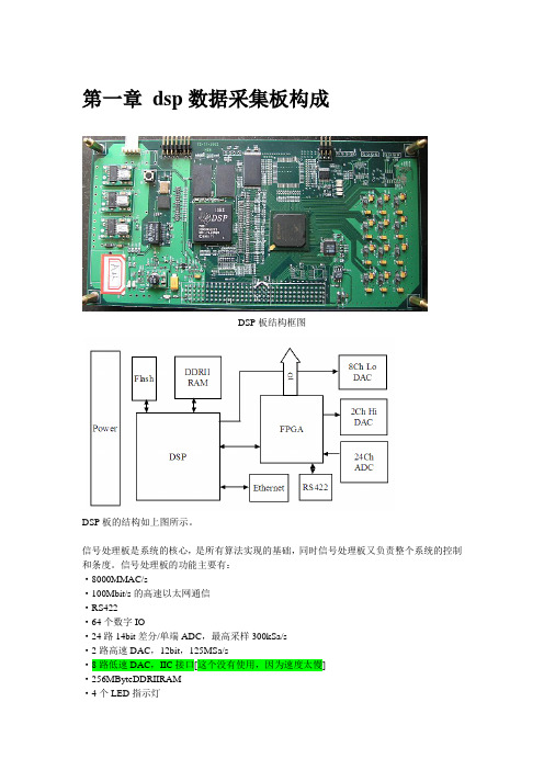
第一章dsp数据采集板构成DSP板结构框图DSP板的结构如上图所示。
信号处理板是系统的核心,是所有算法实现的基础,同时信号处理板又负责整个系统的控制和条度。
信号处理板的功能主要有:·8000MMAC/s·100Mbit/s的高速以太网通信·RS422·64个数字IO·24路14bit差分/单端ADC,最高采样300kSa/s·2路高速DAC,12bit,125MSa/s·8路低速DAC,IIC接口[这个没有使用,因为速度太慢]·256MByteDDRIIRAM·4个LED指示灯1、DSPTMS320C6455的功能框图该平台的核心器件数字信号处理器采用德州仪器最新款的高性能数字信号处理器TMS320C6455。
与以往的数字信号处理器相比,TMS320C6455具有更强大的运算能力和更大的IO带宽。
TMS320C6455工作在1GHz,可实现每秒80亿次乘法累加(MAC),TMS320C6455增加了更多的片内存储器,具有256K的一级程序缓存和256K的一级数据缓存,具有2M的可配置的二级缓存和256K的只读存储器。
TMS320C455采用697脚的BGA 封装。
TMS320C6455不但具有强大的处理能力还有丰富的对外接口,来构成一个完整的应用系统,该信号处理平台的大部分器件都是接在TMS320C6455上的。
TMS320C6455的主要接口如下·64位,133-MHz EMIFA接口可以与同步存储器连接,例如SBSRAM、ZBT SRAM。
也可以同异步存储器实现无缝连接,例如SRAM、FLASH和EEPROM。
该接口还可以和标准同步器件和用户逻辑器件连接,例如FPGA、CPLD、ASICs。
·四个高速串行IO接口·32位DDR2内存接口·32(16)位HPI,32位PCI接口·一个Inter-Integrated Circuit接口·两个MCBSP接口·一个10/100/1000MBPs自适应以太网接口·两个64位的定时器·一个UTOPIA接口·16个通用数字IO口2、FPGAVirtexII1000的资源情况FPGA采用Xinlix公司的Virtex II系列的XC2V1000,该器件的密度为100万门。
- 1、下载文档前请自行甄别文档内容的完整性,平台不提供额外的编辑、内容补充、找答案等附加服务。
- 2、"仅部分预览"的文档,不可在线预览部分如存在完整性等问题,可反馈申请退款(可完整预览的文档不适用该条件!)。
- 3、如文档侵犯您的权益,请联系客服反馈,我们会尽快为您处理(人工客服工作时间:9:00-18:30)。
TMS320C6455高速SRIO接口设计引言数字信号处理技术已广泛应用于通信、雷达、声纳、遥感、图形图像处理和语音处理等领域。
随着现代科技的发展,尤其是半导体工艺的进入深亚微米时代,新的功能强劲的高性能数字信号处理器(DSP)也相继推出,如ADI(美国模拟器件)公司的TigerSHARC系列和TI(德州仪器)公司的C6000系列,但是,要实现对运算量和实时性要求越来越高的DSP 算法,如对基于分数阶傅立叶变换的Chirp信号检测与估计,合成孔径雷达(SAR)成像,高频地波雷达中的自适应滤波和自适应波束形成等算法,单片DSP 仍然显得力不从心。
这些挑战主要涉及两个主题:一是计算能力,指设备、板卡和系统中分别可用的处理资源。
采用多DSP、多FPGA系统,将是提高运算能力的一个有效途径。
二是连接性,从本质上说就是实现不同设备、板卡和系统之间的“快速”数据转移。
对于一些复杂的信息系统,对海量数据传输的实时性提出了苛刻的要求,多DSP之间、DSP与高速AD采集系统、DSP与FPGA间的高速数据传输,是影响信号处理流程的主要瓶颈之一。
TI公司最新推出的高性能TMS320C6455(下文称C6455)处理器,具有高速运算能力的同时集成了高速串行接口SRIO,方便多DSP以及DSP与FPGA之间的数据传输,在一定程度上满足了高速实时处理和传输的要求。
本文在多DSP+FPGA通用信号处理平台的基础上,深入研究了多DSP间,DSP与FPGA间的SRIO 的数据通信和加载技术的软硬件设计与实现。
这些技术包括了目前SRIO接口的各种应用方式,可作为SRIO接口及C6455开发提供参考[1-3]。
1 C6455特性及SRIO标准介绍C6455是目前单片处理能力最强的新型高性能定点DSP,它是TI 公司基于第三代先进VeloviTI VLIW(超长指令字)结构开发出来的新产品。
最高主频为1.2GHz,16位定点处理能力为9600MMAC/s。
C6455建立在增强型C64x+ DSP内核基础之上,代码尺寸平均缩短了20%至30%,周期效率提高了20%。
C6455不仅是内核的增强和运算速度的提升,相比以前的芯片,集成了丰富的外围接口,如千兆以太网控制器,66 MHz PCI总线接口,最重要的是增加了新的外设接口SRIO,全双工工作时,四个端口峰值速率每秒高达25 Gbits,解决了DSP高速数据传输的瓶颈,降低了开发多处理器系统的难度[4-5]。
RapidIO是新一代高速互连技术,已于2004年被国际标准化组织(ISO)和国际电工协会(IEC)批准为ISO/IEC DIS 18372标准。
RapidIO互连定义包括两类技术:面向高性能微处理器及系统互连的Parallel RapidIO接口;面向串行背板、DSP和相关串行控制平面应用的Serial RapidIO接口。
SRIO支持编程模型包括基本存储器映射IO事务、基于端口的消息传递和基于硬件一致性的全局共享分布式处理器。
SRIO互连架构是一个开放的标准,满足了嵌入式基础实施在应用方面的广泛需要。
可行的应用包括多处理器、存储器、网络设备中的存储器映射I/O器件、存储子系统和通用计算平台。
这一互连技术主要作为系统内部互连,支持芯片到芯片和板到板的通信,可以实现从1Gbps到60Gbps的性能水平,在高速互连方面将会有广阔的发展前景[6]。
2 C6455间的SRIO通信2.1 C6455间的接口互连C6455内嵌了SRIO模块,拥有4个全双工的port(端口),支持SRIO 1x/4x串行协议。
每个port支持1.25Gbps、2.5Gbps、3.125Gbps的波特率,每个port可以单独构成1x模式,也可以四个port共同构成4x模式。
SRIO采用的是CML(电流型逻辑)电平,布线时必须遵循布线约束。
为了最小化来自接收方100欧终端电阻的反射,差分对应该具有50欧的阻抗,并且差分走线必须等长。
在接收端串接耦合电容,隔离直流偏置。
图1是两片C6455之间SRIO接口设计。
2.2 包格式SRIO的传输操作是基于请求和响应机制,包(packet)是系统中端点器件的通信单元。
图2是一次传输操作的流程图。
首先由发起者产生一个传输请求,请求包被传输到相邻的交换器件,从而进入交换结构,通过交换机构这个完整的请求包被转发到目标器件。
目标器件根据请求完成相应操作后,发送相应的响应包,经过交换机构传回到发起者。
此时一个完整的传输过程完成。
SRIO有三个层的协议共同组成,每层协议在包中都有体现。
图3给出典型的请求包和响应包的包格式示意图。
请求包以物理层字段开始。
S位指示这是一个包还是一个控制符号,AckID表明交换结构器件将使用控制符号来确认哪一个包,Prio字段指示用于流量控制的包优先级,TT为目标地址和源地址字段指示传输地址的机制类型、报应被递送到的器件的地址和产生包的器件的地址,Ftype表示正被请求的事务,长度字段等于编码后事务的长度,SRIO事务数据的有效载荷长度从1到256字节不等,源事务ID指示发送器件的事务ID,SRIO器件在两个端点器件间最多允许256个未完成的事务。
对于存储器映射事务,跟随在源事务ID后面的是器件偏移地址字段,用于指示数据的存放地址,CRC为校验码。
响应包与请求包类似,状态字段指示是否成功完成了事务,目标事务ID字段的值与请求包中断事务ID字段的值相等。
2.3 SRIO基本读写和门铃操作根据包的格式的不同,将事务划分成很多类型,其中最重要的类型有三种:NREAD(基本读操作)、NWRITE(基本写操作)、DOORBELL(门铃操作)。
通过这三种类型的组合就可以完成所有的存储器读写操作。
在介绍读写操作之前,先介绍一下与SRIO有关的DMA操作。
在C6455上,SRIO数据传输和DMA传输是结合的。
此DMA与EDMA方式是独立的,当进行SRIO传输时,DMA以自动方式启动。
对与发送方来说,DMA将数据从L2 SRAM搬移到SRIO 端口,对于接收方来说,DMA将数据从SRIO端口搬移到L2 SRAM内存。
因此,在进行传输时,读写地址是直接显示在包里的,而且此地址就是被读写的DSP的地址。
换句话说,DSP可以对另一片DSP的L2 SRAM直接进行读写操作。
图4就是自动DMA的传输操作。
读写操作和门铃操作主要由图5中的7个寄存器进行控制,这些寄存器里的值会自动加入到包中。
在SRIO总线上,每个SRIO设备都有一个相应的设备地址,设备地址好比一个SRIO设备的ID,用于区别不同的SRIO设备。
当SRIO总线上的一个SRIO设备进行读写访问时,它发送的包就含有设备地址,只有自身设备地址与包的设备地址符合的SRIO设备才会对此次传输做出响应。
SRIO Address MSB和SRIO Address LSB共同构成64-bit寻址,指示的是被访问SRIO设备的地址。
开发板上只用到32-bit寻址,因此,SRIO Address MSB为0,SRIO Address LSB指示的是被访问的DSP的地址。
DSP address指示的是本地DSP的地址。
Byte_count这一项给出的是传输字节数,一次读写操作(可以是很多包)最多可以传送4Kbytes的数据。
DestID是目标设备的ID号,用来区分SRIO总线上的设备。
Drbll Info用于门铃事件,通过此位段的设置,从而向目标DSP产生中断。
Packet Type用来指示此次传输的类型,例如NREAD、NWRITE和DOORBELL等。
图6是SRIO模块的NREAD、NWRITE和DOORBELL程序编写流程图。
首先初始化SRIO端口,此过程主要需要配置和使能PLL模块,使能并配置接收模块,使能并配置发送模块,使能并配置中断模块。
配置这些模块特别要注意的是使主DSP和从DSP的时钟模块工作在相同的波特率。
初始化完成后,查询SRIO链路是否成功建立,如果SRIO链路没有建立,则重新初始化SRIO端口,直到SRIO链路建立为止。
链路建立后就可以进行读写操作和门铃操作,两片DSP之间可以进行高速的数据传输。
实际测试表明,DSP间的数据传输可工作于1x和4x模式,每种模式可以正常工作于每通道3.125Gbps 的传输速率。
3 C6455间的SRIO加载3.1 C6455引导模式在C6455的地址空间0x00100000到0x00107FFF集成了32K的内部ROM。
此ROM中固化了一段“boot loader”的引导代码,它主要作用是在DSP上电时,对DSP进行必要的配置,以便辅助HPI/PCI/SRIO等接口进行加载;另外,它还可以将代码从外部存储器读到内部L2 SRAM,以完成代码加载。
C6455复位和上电时的引导模式主要有:NO BOOT模式,主机引导模式,FLASH引导模式,主I2C引导模式,从I2C引导模式,SRIO引导模式。
C6455的EMIFA端口引脚EMIFA [0:19]和ABA[1:0]被复用作配置引脚,和专用引脚PCI_EN一起构成C6455的硬件配置引脚。
采用哪种引导模式,由复位或上电时采样管脚BOOTMOOD[3:0]来决定[7-9]。
表1是引导模式选择方式。
对被加载的从DSP来说,设置BOOTMOOD[3:0]=1x00,此时为SRIO引导模式,SRIO被配置成四个1x端口,由port0对从DSP进行加载。
另外,差分晶振选择125M的时钟源。
上电后,固化在从DSP内部ROM的“boot loader”对从DSP进行一些必要的初始化配置:使能全局中断,SRIO的中断管脚被使能,使从DSP可以接收来自主DSP的中断;boot loader配置PLL1模块为15倍频,也就是使内核工作在750MHz;boot loader初始化从DSP的SRIO端口,使SRIO的时钟模块配置成1.25G。
主DSP对SRIO端口进行初始化配置,并将时钟模块配置成1.25G。
此时主DSP与从DSP之间互相发送同步信息,直到链路建立。
链路成功建立以后,主DSP执行NWRITE操作,将待加载程序装载到L2 SRAM内存中。
代码装载完成后,执行门铃操作,向从DSP发送中断,从DSP收到中断后脱离“挂起”状态,从地址0x800000处运行程序,加载过程结束。
图7便是SRIO引导过程。
实测表明,主DSP通过FLASH加载完成后,可通过SRIO接口对从DSP完成加载。
4 C6455与FPGA等构建SRIO网络SRIO与微处理器总线类似,它在硬件中完成存储器和器件寻址以及分组处理,降低了用于I/O 处理的开销,减小了延迟。
一个运行于3.125 Gbps的4通道SRIO链路能在完全保持数据完整性的前提下提供25 Gbps的流量,保障了海量数据传输的实时性。