COMSOL光学仿真专题
基于COMSOL软件的谐振腔仿真与分析

基于COMSOL软件的谐振腔仿真与分析闵力; 魏勇; 田芃; 王文进【期刊名称】《《电子世界》》【年(卷),期】2019(000)019【总页数】2页(P55-56)【作者】闵力; 魏勇; 田芃; 王文进【作者单位】湖南理工学院物理与电子科学学院【正文语种】中文以矩形谐振腔为例,理论推导了谐振腔内部电磁场分布及品质因子,并利用COMSOL软件进行了仿真验证。
结果表明,该软件仿真结果与理论计算结果高度一致,且能够直观、形象地展现谐振腔内部电磁参数分布。
1 前言电磁谐振腔其工作原理类似于无线LC振荡回路,不仅可用来产生高频率的振荡信号,在微波技术方面还有着广泛的应用(周俊,刘大刚,曾亚文,et al.微波谐振腔本征模求解的算法及应用:材料导报,2007),如:选频元件,波长计和滤波器等。
关于谐振腔的电磁理论,解析法只能对几种特殊结构谐振腔求解;此外,传统教学一般是通过求解麦克斯韦方程来讲解,其过程复杂而又繁琐,多数课堂会弱化这部分知识教学,学生也会望而生畏,失去了学习的兴趣。
这些导致学生对这方面的认识不够,实际工程应用能力普遍较差。
COMSOL软件属于一种多物理场仿真软件,其中包含了专门用于射频和微波建模仿真的RF模块,该模块能够对各种结构光学器件进行仿真(马愈昭,许明妍,范懿,et al.基于COMSOL4.2的波导模式特性仿真:电气电子教学学报,2015);除此外,该软件丰富的后处理功能还可让抽象的电磁现象更加直观具体(陈庆东,王俊平,基于COMSOL软件的静磁场仿真与分析:大学物理实验,2018;周子杰,刘英伟,张洋,et al.实用COMSOL后处理二次开发技术:科技与创新,2018)。
本文通过该软件直观地展现了矩形谐振腔内部电磁场分布,并自动计算了谐振腔的品质因子;另外,还与理论计算结果进行了对比分析。
该方式能够让学生更加形象地理解谐振腔电磁特性,激发学生的学习兴趣。
图1 矩形谐振腔2 谐振腔TE模式下电磁理论推导矩形谐振腔结构如图1所示,沿x轴方向内腔边长为a,沿y轴方向内腔边长为b,沿z轴方向内腔边长为c,谐振腔内部填充空气,谐振腔壁为理想导体。
comsol单模光纤仿真案例
comsol单模光纤仿真案例Step-Index FiberIntroductionThe transmission speed of optical waveguides is superior to microwave waveguides because optical devices have a much higher operating frequency than microwaves, enabling a far higher bandwidth.Today the silica glass (SiO 2) fiber is forming the backbone of modern communication systems. Before 1970, optical fibers suffered from large transmission losses, making optical communication technology merely an academic issue. In 1970, researchers showed, for the first time, that low-loss optical fibers really could be manufactured. Earlier losses of 2000 dB/km now went down to 20 dB/km. Today’s fibers have losses near the theoretical limit of 0.16 dB/km at 1.55 μm (infrared light).One of the winning devices has been the single-mode fiber, having a step-index profile with a higher refractive index in the center core and a lower index in the outer cladding. Numerical software plays an important role in the design of single-mode waveguides and fibers. For a fiber cross section, even the most simple shape is difficult and cumbersome to deal with analytically.A circular step-index waveguide is a basic shape where benchmark results are available (see Ref. 1).This example is a model of a single step-index waveguide made of silica glass. The inner core is made of pure silica glass with refractive index n 1 = 1.4457 and the cladding is doped, with a refractive index of n 2 = 1.4378. These values are valid for free-space wavelengths of 1.55 μm. The radius of the cladding is chosen to be large enough so that the field of confined modes iszero at the exterior boundaries.For a confined mode there is no energy flow in the radial direction, thus the wave must be evanescent in the radial direction in the cladding. This is true only ifOn the other hand, the wave cannot be radially evanescent in the core region. ThusThe waves are more confined when n eff is close to the upper limit in this interval.n eff n 2>n 2n eff n 1<<Model DefinitionThe mode analysis is made on a cross-section in the xy -plane of the fiber. The wave propagates in the z direction and has the formwhere ω is the angular frequency and β the propagation constant. An eigenvalue equation for the electric field E is derived from Helmholtz equationwhich is solved for the eigenvalue λ = ?j β.As boundary condition along the outside of the cladding the electric field is set to zero. Because the amplitude of the field decays rapidly as a function of the radius of the cladding this is a valid boundary condition.Results and DiscussionWhen studying the characteristics of optical waveguides, the effective mode index of a confined mode,as a function of the frequency is an important characteristic.A common notion is the normalized frequency for a fiber. This is defined aswhere a is the radius of the core of the fiber. For this simulation, the effective mode index for the fundamental mode,1.4444 corresponds to a normalized frequency of4.895. The electric and magnetic fields for this mode is shown in Figure 1 below.E x y z t ,,,()E x y ,()e j ωt βz –()=??E ×()×k 02n 2E –0=n eff βk 0-----=V 2πa λ0----------n 12n 22–k 0a n 12n 22–==Figure 1: The surface plot visualizes the z component of the electric field. This plot is for the effective mode index 1.4444.Reference1. A. Yariv, Optical Electronics in Modern Communications, 5th ed., Oxford University Press, 1997.Model Library path:RF_Module/Tutorial_Models/step_index_fiberModeling InstructionsFrom the File menu, choose New.N E W1In the New window, click Model Wizard.M O D E L W I Z A R D1In the Model Wizard window, click 2D.2In the Select physics tree, select Radio Frequency>Electromagnetic Waves, Frequency Domain (emw).3Click Add.4Click Study.5In the Select study tree, select Preset Studies>Mode Analysis.6Click Done.G E O M E T R Y11In the Model Builder window, under Component 1 (comp1) click Geometry 1.2In the Settings window for Geometry, locate the Units section.3From the Length unit list, choose μm.Circle 1 (c1)1On the Geometry toolbar, click Primitives and choose Circle.2In the Settings window for Circle, locate the Size and Shape section.3In the Radius text field, type 40.4Click the Build Selected button.Circle 2 (c2)1On the Geometry toolbar, click Primitives and choose Circle.2In the Settings window for Circle, locate the Size and Shape section.3In the Radius text field, type 8.4Click the Build Selected button.M A T E R I A L SMaterial 1 (mat1)1In the Model Builder window, under Component 1 (comp1) right-click Materials and choose Blank Material.2Right-click Material 1 (mat1) and choose Rename.3In the Rename Material dialog box, type Doped Silica Glass in the New label text field.4Click OK.5Select Domain 2 only.6In the Settings window for Material, click to expand the Material properties section. 7Locate the Material Properties section. In the Material properties tree, select Electromagnetic Models>Refractive Index>Refractive index (n).8Click Add to Material.9Locate the Material Contents section. In the table, enter the following settings:Property Name Value Unit Property groupRefractive index n 1.44571Refractive indexMaterial 2 (mat2)1In the Model Builder window, right-click Materials and choose Blank Material.2Right-click Material 2 (mat2) and choose Rename.3In the Rename Material dialog box, type Silica Glass in the New label text field. 4Click OK.5Select Domain 1 only.6In the Settings window for Material, click to expand the Material properties section. 7Locate the Material Properties section. In the Material properties tree, select ElectromagneticModels>Refractive Index>Refractive index (n).8Click Add to Material.9Locate the Material Contents section. In the table, enter the following settings:Property Name Value Unit Property groupRefractive index n 1.43781Refractive indexE L E C T R O M A G N E T I C W A V E S,F R E Q U E N C Y D O M A I N(E M W)Wave Equation, Electric 11In the Model Builder window, expand the Component 1 (comp1)>Electromagnetic Waves, Frequency Domain (emw) node, then click Wave Equation, Electric 1.2In the Settings window for Wave Equation, Electric, locate the Electric Displacement Field section.3From the Electric displacement field model list, choose Refractive index.M E S H11In the Model Builder window, under Component 1 (comp1) click Mesh 1.2In the Settings window for Mesh, locate the Mesh Settings section.3From the Element size list, choose Finer.4Click the Build All button.S T U D Y1Step 1: Mode Analysis1In the Model Builder window, under Study 1 click Step 1: Mode Analysis.2In the Settings window for Mode Analysis, locate the Study Settings section.3In the Search for modes around text field, type 1.446. Themodes of interest have an effective mode index somewhere between the refractive indices of the two materials. The fundamental mode has the highest index. Therefore, setting the mode index to search around to something just above the core index guarantees that the solver will find the fundamental mode.4In the Mode analysis frequency text field, type c_const/1.55[um]. This frequency corresponds to a free space wavelength of 1.55 μm.5On the Model toolbar, click Compute.R E S U L T SElectric Field (emw)1Click the Zoom Extents button on the Graphics toolbar.2Click the Zoom In button on the Graphics toolbar.3The default plot shows the distribution of the norm of the electric field for the highest of the 6 computed modes (the one with the lowest effective mode index).To study the fundamental mode, choose the highest mode index. Because the magnetic field is exactly 90 degrees out of phase with the electric field you can see both the magnetic and the electric field distributions by plotting the solution at a phase angle of 45 degrees.Data Sets1In the Model Builder window, expand the Results>Data Sets node, then click Study 1/ Solution 1.2In the Settings window for Solution, locate the Solution section.3In the Solution at angle (phase) text field, type 45.Electric Field (emw)1In the Model Builder window, under Results click Electric Field (emw).2In the Settings window for 2D Plot Group, locate the Data section.3From the Effective mode index list, choose 1.4444 (2).4In the Model Builder window, expand the Electric Field (emw) node, then click Surface 1.5In the Settings window for Surface, click Replace Expression in the upper-right corner of the Expression section. From the menu, choose Model>Component1>Electromagnetic Waves, Frequency Domain>Electric>Electric field>emw.Ez - Electricfield, z component.6On the 2D plot group toolbar, click Plot.Add a contour plot of the H-field.7In the Model Builder window, right-click Electric Field (emw) and choose Contour.8In the Settings window for Contour, click Replace Expressionin the upper-right corner of the Expression section. From the menu, choose Model>Component1>Electromagnetic Waves, Frequency Domain>Magnetic>Magnetic field>emw.Hz -Magnetic field, z component.9On the 2D plot group toolbar, click Plot. The distribution of the transversal E and H field components confirms that this is the HE11 mode. Compare the resulting plot with that in Figure 1.。
基于COMSOL的HID灯物理模型

基于COMSOL的HID灯物理模型【摘要】本文介绍了基于COMSOL的HID灯物理模型。
我们阐述了研究背景和研究意义。
接着,详细解释了HID灯的工作原理以及COMSOL在光学仿真中的应用。
然后,我们描述了如何使用COMSOL建立HID灯的光学模型,并对模型进行了分析和光学参数优化。
结论部分讨论了基于COMSOL的HID灯光学模型的可靠性,对HID灯设计的启示,以及未来的展望。
这篇文章对于研究者和工程师在设计和优化HID灯方面具有重要参考价值。
【关键词】HID灯、COMSOL、光学仿真、光学模型、光学参数、优化、可靠性、设计、未来展望1. 引言1.1 研究背景研究背景:HID灯(高强度气体放电灯)是一种高效、高亮度的照明设备,广泛应用于汽车大灯、室外照明等领域。
随着LED等新光源技术的发展,HID灯的照明效果与能效比逐渐受到挑战。
对HID灯的光学性能进行深入研究和优化已成为当今照明行业的热点问题。
基于COMSOL来建立HID灯的光学模型,对于深入了解其光学性能、提高设计效率、降低成本具有重要意义。
通过模拟分析HID灯的光学参数,能够优化灯具结构,提高其光效和光质,为照明行业的发展带来新的启示。
1.2 研究意义HID灯作为目前常见的一种高效、高亮度照明设备,广泛应用于街道照明、工业照明等领域。
随着人们对照明质量和节能环保要求的不断提高,对HID灯的设计和优化也显得尤为重要。
基于COMSOL的HID灯物理模型可以帮助我们更深入地了解HID灯的光学特性,优化其光学参数,提高照明效果和能效比。
通过建立基于COMSOL的HID 灯光学模型,可以实现对HID灯光束形状、亮度分布等关键参数的精确模拟和优化,为HID灯的设计和制造提供重要参考。
研究基于COMSOL的HID灯光学模型具有重要的实际意义和应用前景,将有助于推动HID灯的发展,提高其在照明领域的竞争力。
2. 正文2.1 HID灯的工作原理HID灯(High Intensity Discharge lamp)是一种高强度放电灯,也称为气体放电灯。
基于comsol的仿真实验
一、实验目的熟悉掌握COMSOL Multiphysics软件,通过3D有限元建模方法,建立铂电极-玻璃体-视网膜的分层电刺激模型。
深入研究电极如何影响电刺激效果,系统的分析了电极尺寸、电极到视网膜表面的距离等参数对视网膜电刺激的影响,为视网膜视觉假体刺激电极的刺激效果提供指导意义,进一步优化电刺激效果,达到提高人工视觉的修复效果。
二、实验仪器设备计算机,COMSOL Multiphysics软件三、实验原理影响视网膜电刺激效果的因素有许多:电极尺寸、电极距视网膜距离、电极形状、电极排列等,这里主要从电极尺寸,电极距视网膜距离来探讨。
视网膜电刺激模型通过参考视网膜解剖结构构建,电刺激的有效响应区域取决于神经节细胞层(GCL)电场强度是否大于1000V/m,当大于该值时认为该区域神经节细胞能够兴奋,进而指导电极尺寸、电极距视网膜距离的参数。
四、实验内容根据视网膜的解剖结构来构建相应的视网膜分层模型,模型总共分为8层:玻璃体层,神经节细胞层,内网状层,内核层,外网状层,外核层,视网膜下区域,色素上皮层,脉络膜及巩膜。
根据视网膜各层的导电特性来设定相应的导电率,模型构建,设置边界条件。
在电极处施加相应电流刺激,规定神经节细胞层(GCL)电场强度(>1000V/m)时认为能够引起视神经细胞兴奋,在确定的电流强度下,神经节细胞层(GCL)层电场强度大于1000V/m的区域认为有效响应区域,进而判断电极刺激的有效响应区域,指导电极尺寸r和电极距视网膜距离h等参数设置。
其具体实验步骤如下所示:1、根据视网膜的解剖特性构建视网膜分层模型。
模型在三维模式下电磁场子目录下的传导介质DC场下建立。
进入建模窗口后,在绘图栏下设置模型为圆柱体,输入各部分的长宽高数值,轴基准点为圆柱体的圆心坐标。
模型分为9层(11个求解域),其示图如下:图1 视网膜分层模型2、模型建好后,在菜单栏下的物理量里面选择求解域设定,对示图的11个求解域进行设定传导率,如图2所示,其中每一层的电导率情况参考于视网膜导电特性。
新工科背景下光通信课程comsol仿真实验设计与实施

摘 要:“新工科”这一概念提出以来,教育部组织高校进行深入研讨,形成了“复旦共识”,“天大行动”和“北京指南”。
之后便逐步开启了新工科建设的大幕,新工科建设步入了实质性的具体实施阶段。通过新工科研究与实践项目的组织和实
施,来全方位、多角度地深入扎实推进新工科建设。在新工科建设的要求下,本文通过引入多物理场分析软件结合国际研
科技创新导报 2019 NO.29 Science and Technology Innovation Herald
DOI:10.16660/ki.1674-098X.201背景下光通信课程Comsol仿真实验设计 与实施①
赵健 (天津大学精密仪器与光电子工程学院光电信息技术教育部重点实验室 天津 300072 )
随后在拉锥比为04015之间时如图5b所示拉锥的进行使得光子灯笼的直径逐步减小熔融拉锥慢慢损坏了原本光纤结构原本各光纤中的光场无法再被束缚在纤芯之中原本的模式逐渐进入包层之中此时原本的包层变成新的纤芯a值变大纤芯的归一化频率回到的状态包层中支持多种图4三模光子灯笼支持模式的有效折射率曲线科技创新导报2019no29scienceandtechnologyinnovationherald创新教育科技创新导报scienceandtechnologyinnovationherald219模式的存在
1 新工科实施的背景与意义 教育 部曾多 次召开 高等工 程 教育相 关 研 讨会,提 出了
新工 科 建 设 要求,并已达 成“复 旦共识”、“天大 行 动”和 “北 京指南”,旨在 通 过 新工 科 建 设,推动人 才 培 养 模 式 等 方面的改革。新工 科 建 设 是 一项涉及面广、影响面宽、 具有中国特色的复杂的系统工程,对中国高等教育的改革 和发展具有示范和引领作用。未来的竞争是科技的竞争、 人 才的 竞 争,以人 工智能、量 子 信息、区块 链为代 表的新 科 技的迭 代 升 级 越 来 越快。为主动应 对 新 一轮 科 技革命 与产业变革,加快建设发展新工科,探索形成中国特色、 世界水平的工程教育体系,促进我国从工程教育大国走向 工 程 教育 强国,教育 部 牵头 推出了“ 六卓越 一 拔 尖”计 划 2 . 0。天津 大 学作为 新工 科的“领 头雁”,在 全国率先 发布 “天津大学新工科建设方案”,旨在为新工科建设提供新 范式,为世界新工科建设提供“天大经验”、贡献“天大模 式”。为了积 极响 应学 校的号召,本 文 通 过 光 通信 技 术 基 础这门课程的改革,开展了基于Comsol多物理场仿真软件 对国际研 究 热点-光 子 灯笼的仿真实验,为新工科建 设 进
comsol仿真高斯光束
3 |
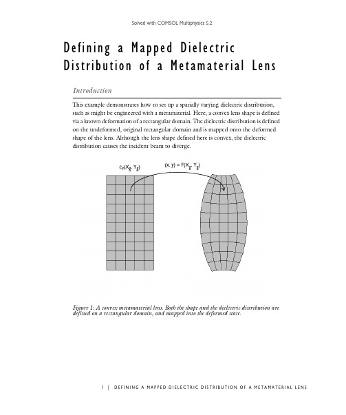
DEFINING A MAPPED DIELECTRIC DISTRIBUTION OF A METAMATERIAL LENS
Solved with COMSOL Multiphysics 5.2
Figure 3: The norm of the electric field shows the Gaussian beam diffracted by the metamaterial lens.
1 |
DEFINING A MAPPED DIELECTRIC DISTRIBUTION OF A METAMATERIAL LENS
Solved with COMSOL Multiphysics 5.2
Model Definition
Consider a 2D model geometry as shown in Figure 2. A square air domain, bounded by a perfectly matched layer (PML) on all sides, encloses a rectangular region in which the metamaterial lens is defined.
Figure 4: Contour plot of the dielectric distribution.
4 |
DEFINING A MAPPED DIELECTRIC DISTRIBUTION OF A METAMATERIAL LENS
Solved with COMSOL Multiphysics 5.2
2 |
DEFINING A MAPPED DIELECTRIC DISTRIBUTION OF A METAMATERIAL LENS
Comsol经典实例012:高斯波速的二次谐波产生

Comsol经典实例012: 高斯波速的二次谐波产生激光系统是现代电子技术中的一个重要应用领域。
激光束的生成方法有很多种, 这些方法有个共同点: 波长由受激发射决定, 而受激发射取决于材料参数。
通常很难生成具有短波长的激光。
但是, 如果使用非线性材料, 就有可能产生频率为激光频率数倍的谐波。
通过使用二阶非线性材料可生成波长为基频光束波长一半的相干光。
本案例演示了如何设置非线性材料属性, 通过瞬态波仿真产生二次谐波。
模型中一束波长为1.06μm的激光聚焦于非线性晶体, 光束的腰部落于晶体内。
在激光的传播过程中, 大部分能量都集中在传播轴附近, 在求解麦克斯韦方程时可以近轴近似, 由此获得高斯波束。
一、物理场选择及预设研究Step01: 打开comsol软件, 单击“模型向导”选项创建模型, 在模型的“选择空间维度”界面选择“二维”, 在“选择物理场”界面分别选择“光学→波动光学→电磁波, 瞬态(ewt)”, 单击“添加”按钮。
对应变量设置完毕以后, 单击“研究”按钮, 在“选择研究”树中添加“预设研究”中的“瞬态”研究, 单击“完成”按钮进入软件主界面, 如图1所示。
图1 软件主界面二、全局定义1.参数Step02: 参数设置。
在模型开发器窗口的全局定义节点下, 单击“参数”子节点, 在“参数”设置窗口中, 定位到“参数”栏, 输入如图2所示的参数。
图2 设置全局参数2.解析定义Step03: 在“主屏幕”工具栏中单击“函数”选项, 在下拉菜单中选择“全局→解析”选项。
单击“解析1”子节点, 在“解析”设置窗口中, 定位到“函数名称”栏, 在文本输入框中输入“w”;定位到“定义”栏, 在“表达式”文本输入框中输入“w0*sqrt(1+(x/x)^2)”;定位到“单位”栏, 在“变元”文本输入框中输入“m”, 在“函数”在文本输入框中输入“m”,如图3所示。
Step04:在“主屏幕”工具栏中单击“函数”选项, 在下拉菜单中选择“全局→解析”选项。
COMSOL二维膜层光学性能-吸收率仿真教学
COMSOL⼆维膜层光学性能-吸收率仿真教学COMSOL⼆维膜层结构光学性能/吸收率仿真教学新建
1. 新建→模型向导→⼆维;
2. →选择物理场:光学→波动光学→电磁波,频域→增加→研究;
3. 选择研究:波长域→完成;
建模
4. ⼏何绘制多个长⽅形形成多层膜结构;
5. 必要的情况下可以在上下层加⼊空⽓层(真空层);
边界条件
6. 添加“端⼝”,设置红外⼊射端⼝,在空⽓层边界上。
再添加“端⼝”,设置出射端⼝,另⼀端的空⽓层;
7. 模型两侧边界设置为“周期性边界条件”;
8. 对于膜层很薄的部分,可以设置为“过渡边界条件”,代替超薄层,厚度可在此条件下设置;
9. 进⾏⽹格化;
材料参数
10. 顶部⼯具栏:增加材料;
11. 可在右侧框内搜索要添加的材料,然后“增加到选择”;或者添加空材料,去选择⼀个域,然后材料属性⽬录下会出现做该仿真必要的参数,输⼊参数即可;研究:结果
12. 研究→波长域,设置波长范围及步长,点击“研究”;
13. 派⽣值→全局计算,表达式选“ewfd.Atotal” ;数据系列运算选“⽆”,计算;仿真图下⽅出现“表格”,得到“波长”与“吸收率”关系。
点击“表图”按钮,得到“吸收曲线”;
14. 派⽣值→全局计算,表达式选“ewfd.Atotal”;数据系列运算选“平均值”,计算;仿真图下⽅出现“表格”,得到“平均吸收率”值。
- 1、下载文档前请自行甄别文档内容的完整性,平台不提供额外的编辑、内容补充、找答案等附加服务。
- 2、"仅部分预览"的文档,不可在线预览部分如存在完整性等问题,可反馈申请退款(可完整预览的文档不适用该条件!)。
- 3、如文档侵犯您的权益,请联系客服反馈,我们会尽快为您处理(人工客服工作时间:9:00-18:30)。
透镜的受热变形
空气/真空
TE10 波导
(未显示) 4µm 宽 “准直” 透镜 PML无反射 截止域
仿 真 智 领 创 新
Simulating inspires innovation
ቤተ መጻሕፍቲ ባይዱ
局部温度
折射率
透镜变形
10 µ-sec 1 ms 100 ms 1 sec
负折射现象
负折射材料
介电常数e和磁导率m均为负数
隐形斗篷
仿 真 智 领 创 新
Simulating inspires innovation
负折射率铁磁流体
Y. Gao, J. P. Huang, Y. M. Liu, L. Gao, K. W. Yu, and X. Zhang, PRL 104, 034501 (2010)
COMSOL Multiphysics
光学系统与微纳光学专题
中仿科技 鲍伟(Feit Bao) 2013年1月
仿 真 智 领 创 新
Simulating inspires innovation
光学理论研究方法 • 几何光学:
– 波长 << 特征尺寸 – 光线追迹
• 波动光学:
– 波长与特征尺寸可比拟 – 有限时域差分方法 – 时域有限元方法
仿 真 智 领 创 新
Simulating inspires innovation
总结
• COMSOL RF模块可满足纳米光子学研究中的 以下需求:
– 波导模式分析 – 稳态传输特性分析 – 瞬态传输特性分析
• COMSOL支持进一步的研究需求
– 支持用户自定义PDEs,处理量子光学问题(薛定谔 方程的求解) – 多物理场耦合,光与物质的相互作用(原子冷却、 粒子囚禁与操控等)
仿 真 智 领 创 新
Simulating inspires innovation
高双折射光子晶体光纤
• 非对称椭圆形空气孔 • 双折射度
Han-Hsuan Yeh, Yuan-Fong Chau 清云科技大学电子工程系
仿 真 智 领 创 新
Simulating inspires innovation
仿 真 智 领 创 新
Simulating inspires innovation
3. 稳态传输特性分析
• 针对问题: – 超材料/负折射材料传输特性 – 波导器件传输特性 – 光栅/金属颗粒散射 – 光刻分辨率分析 • 预置电磁场频域分析应用模式 • 自定义光源入射条件 • 后处理 – 内置反射/透射率计算 – 散射场分布
仿 真 智 领 创 新
Simulating inspires innovation
COMSOL Multiphysics 在此领域享有盛誉
“(在纳米光子学领域)FEM被广泛用于求解电磁 问题,源于一款受欢迎的商业软件:COMSOL Multiphysics。” —Nanophotonics Accessibility and Applicability, the
电磁波领域研究课题
• 电磁波的产生
– 各种波源的辐射机制
• 电磁波的传播
– 衍射/干涉 – 反射/折射/散射/吸收 – 光电/热/力效应
仿 真 智 领 创 新
Simulating inspires innovation
数值分析
• 散射分析
– 散射强度 – 透射/反射率
• 波导分析
– 模式:场分布,传播常数 – 透射/反射率
光子晶体光纤SPP传感器
∧=2e-6m, dc=0.5 ∧, d1=0.6 ∧, d2=0.8 ∧ nair=1.0, na=1.33 金属层厚度4e-8m
基模
仿 真 智 领 创 新
Simulating inspires innovation
光子晶体光纤SPP传感器
纤芯中激发的SPP模式图
金属层表面能量分布图
仿 真 智 领 创 新
Simulating inspires innovation
COMSOL在《Nature》中论文发表量
30 25
20
15 10 5 0 2003 2004 2005 2006 2007 2008 2009 2010 2011
仿 真 智 领 创 新
Simulating inspires innovation
• 粒子追踪现在是可用的物理接口:
– – – – – – – – – – 利用COMSOL求解基于有限元问题的强大求解器 轻松模拟成百上千的粒子 能使用参数扫描 可指定粒子的边界条件 解储存于模型而非在后处理时计算 隐式时间步进 支持粒子/场相互作用 预定义力作为模型树中可用特征 Hamilton算子允许模拟光线追踪 新的后处理工具
4. 时域传输特性分析
• 针对问题
– 瞬态及非线性过程分析 – 金属颗粒表面场增强拉曼散射 分子荧光成像/二次谐波产生
• • • •
预置时域分析应用模式 自定义材料非线性极化率 自定义入射光源的时空分布 后处理
– 时域传输过程动画导出
仿 真 智 领 创 新
Simulating inspires innovation
仿 真 智 领 创 新
Simulating inspires innovation
隐形斗篷
隐形斗篷
超材料制成,使斗篷内的物体在微波波段不可见。 这项基于COMSOL Multiphysics仿真分析的研究工作,由北卡罗 来州达拉莫杜克大学的Steve. Cummer和David. Schurig共同完 成,被Science杂志评为2006年科学突破之一。
COMSOL在《Nature》中论文发表量
119
仿 真 智 领 创 新
Simulating inspires innovation
COMSOL典型光学用户
仿 真 智 领 创 新
Simulating inspires innovation
联系我们
中仿科技官方网站: 免费技术交流社区: 服务电话:400-888-5100 电子邮件:Nathan@ 技术服务:Support@ 软件试用及资料申请:democd@
COMSOL Multiphysics Version 4.0 multiphysics simulation software features a new COMSOL Desktop™ user interface that provides an organized layout and streamlined model building. Quick model setup is enabled in the Model Builder and its graphical programming utility throughout the modeling and simulation process. With the new version, a series of LiveLink™ options integrate the software into the mainstream product design workflow of Autodesk® Inventor®, SolidWorks®, and MATLAB®.
高斯光束的二倍频
仿 真 智 领 创 新
Simulating inspires innovation
四波混频计算结果
仿 真 智 领 创 新
Simulating inspires innovation
Duffing模型处理非线性色散
电子作为阻尼非谐振子:
阻尼
非线性
色散
谐振
磁化系数(折射率)
a = 0,Lorentz色散模型
• 腔模分析
– 共振频率 – 品质因子
• 瞬态传播/非线性效应
– 群速度(色散) – 倍频产生、自聚焦、自相位调制等
• 多场耦合
– 光与热,电,磁,力特性的耦合
仿 真 智 领 创 新
Simulating inspires innovation
纳米光子学仿真需求
纳米材料/结构的 光学特性 纳米光子学器件 纳米光子学 光纤/波导 波导分析 激光器 隐形斗篷 稳态传输特性分析 光刻 纳米结构的 光学制备、表征方法 光镊/光势阱 分子探测 瞬态/非线性效应分析
2. 谐振腔模式分析
• 针对问题:
– 各种谐振腔的模式计算 – 品质因子分析
• 预置电磁场特征频率分析应用模式 • 后处理
– 内置品质因子计算 – 模场分布 – 传播常数/有效折射率
仿 真 智 领 创 新
Simulating inspires innovation
仿 真 智 领 创 新
Simulating inspires innovation
Luneburg透镜
磁透镜
四极质谱仪
仿 真 智 领 创 新
Simulating inspires innovation
光学隐身
仿 真 智 领 创 新
Simulating inspires innovation
Luneburg透镜
仿 真 智 领 创 新
Simulating inspires innovation
RF模块理论基础
• RF = Radio Frequency (Electromagnetic Waves), 3kHz~300GHz • 高频电磁波 电尺寸=结构尺寸/波长>1/100 • 基于经典Maxwell电磁理论
时域分析
频域分析
仿 真 智 领 创 新
Simulating inspires innovation
• 时域分析 • 频域分析