UHF常用芯片汇总
UHF常用芯片汇总

UHF常用芯片汇总以下是一些常用的UHF(Ultra High Frequency)芯片的汇总,这些芯片主要用于无线通信和RFID(Radio Frequency Identification)应用。
1. Impinj Monza系列Impinj Monza系列芯片是全球最著名的UHF RFID芯片之一、这个系列提供了高性能、高度集成、低功耗的解决方案。
Monza系列的芯片通常用于物联网、零售、物流和库存管理等领域。
2.NXPUCODE系列NXPUCODE系列芯片是业界最常见的UHFRFID芯片之一、这个系列的芯片具有卓越的性能和可靠性,支持多协议,能够满足不同应用的需求。
UCODE芯片广泛应用于零售、物流、运输和电子票务等领域。
3. Alien Higgs系列Alien Higgs系列芯片是另一个广受欢迎的UHF RFID芯片。
这个系列的芯片采用先进的射频和数字电路技术,具有高度集成、低功耗和高性能的特点。
Higgs芯片常用于零售、制造业、医疗和物流等领域。
4. STMicroelectronics ST25系列ST25系列芯片由STMicroelectronics推出,是一款多功能的UHF RFID芯片。
该系列的芯片具有高度集成、低功耗和优秀性能等特点。
ST25系列芯片广泛应用于物联网、安全识别、物流和库存管理等领域。
5. TI Tag-it系列TI Tag-it系列芯片是德州仪器(Texas Instruments)推出的UHF RFID芯片。
这个系列的芯片具有高度集成、低功耗和高性能的特点,能够满足不同应用领域的需求。
Tag-it芯片常用于物流、库存管理和电子车牌等领域。
6. Smartrac Frog系列7. SensThys SensArray系列SensThys SensArray系列芯片是一种集成射频前端和数字电路的UHF RFID芯片。
这个系列的芯片具有高度灵活性和可扩展性,适用于不同射频环境下的部署和应用。
UHF RFID芯片 AS3990-AS3991芯片资料
AS3990/AS3991UHF RFID Single Chip Reader EPC Class1 Gen2 CompatibleD a ta S h e e t1 General DescriptionThe AS3990/AS3991 UHF reader chip is an integrated analog front end and protocol handling systems for a ISO18000-6C 900MHz RFID reader system.Equipped with built-in programming options, the device is suitable for a wide range of UHF RFID applications. The R901G includes improved on-board VCO and internal PA.The reader configuration is achieved by selecting the desired protocol in control registers. Direct access to all control registers allows fine tuning of different reader parameters.Parallel or serial interface can be selected forcommunication between the host system (MCU) and the reader IC. When hardware coders and decoders are used for transmission and reception, data is transferred via 24 bytes FIFO register.In case of direct transmission or reception, coders and decoders are bypassed and the host system can service the analog front end in real time.The transmitter generates 20dBm output power into 50Ω load and is capable of ASK or PR-ASK modulation. The integrated supply voltage regulators ensure supply rejection of the complete reader system.The transmission system comprises low level datacoding. Automatic generation of FrameSync, Preamble, and CRC is supported.The receiver system allows AM and PM demodulation. The receiver also comprises automatic gain control option (patent pending) and selectable gain and signal bandwidth to cover a range of input link frequency and bit rate options.The signal strength of AM and PM modulation is measured and can be accessed in RSSI register.The receiver output is selectable between digitized sub-carrier signal and any of integrated sub-carrierdecoders. Selected decoders deliver bit stream and data clock as outputs.The receiver system also comprises framing system. This system performs the CRC check and organizes the data in bytes. Framed data is accessible to the host system through a 24 byte FIFO register.To support external MCU and other circuitry a 3.3V regulated supply and clock outputs are available. The regulated supply has 20mA current capability.The AS3990/AS3991 is available in a 64-pin QFN (9mm x 9mm), ensuring the smallest possible footprint.2 Key FeaturesISO18000-6C (EPC Gen2) full protocol support ISO18000-6A,B compatibility in direct mode Integrated low level transmission coding Integrated low level decoders Integrated data framing Integrated CRC checkingParallel 8-bit or serial 4-pin SPI interface to MCUusing 24 bytes FIFOVoltage range for communication to MCU between1.8V and 5.5VSelectable clock output for MCUIntegrated supply voltage regulator (20mA), whichcan be used to supply MCU and other external circuitryIntegrated supply voltage regulator for the RF outputstage, providing rejection to supply noiseInternal power amplifier (20dBm) for short rangeapplicationsModulator using ASK or PR-ASK modulation Adjustable ASK modulation index AM & PM demodulation ensuring no“communication holes” with automatic I/Q selectionBuilt-in reception low-pass and high-pass filters having selectable corner frequenciesSelectable reception gain Reception automatic gain controlAD converter for measuring TX power usingexternal RF power detectorDA converter for controlling external power amplifier Frequency hopping supportOn-board VCO and PLL covering complete RFIDfrequency range 840MHz to 960MHzOscillator using 20MHz crystal Power down, standby and active mode Can be powered by USB with no need for stepconversion3 ApplicationsThe device is an ideal solution for UHF RFID readersystems and hand-held UHF RFID readers.Figure 1. Block DiagramContents1 General Description (1)2 Key Features (1)3 Applications (1)4 Pin Assignments (5)Pin Descriptions (5)5 Absolute Maximum Ratings (8)6 Electrical Characteristics (9)7 Detailed Description (11)Supply (11)Power Modes (12)Host Communication (13)VCO and PLL (13)VCO and External RF Source (13)PLL (13)Chip Status Control (14)Protocol Control (14)Option Registers Preset (14)Transmitter (14)Normal Mode (14)Direct Mode (16)Modulator (17)Amplifier (17)Receiver (18)Input Mixer (18)RX Filter (18)RX Gain (19)Received Signal Strength Indicator (RSSI) (19)Reflected RF Level Indicator (19)Normal Mode (19)Direct Mode (21)Normal Mode With Mixer DC Level Output And Enable RX Output Available (21)ADC / DAC (21)DA Converter (21)AD Converter (22)Reference Oscillator (22)8 Application Information (23)Configuration Registers Address Space (23)Main Configuration Registers (24)Control Registers - Low Level Configuration Registers (25)Status Registers (30)Test Registers (32)PLL, Modulator, DAC, and ADC Registers (33)RX Length Registers (37)FIFO Control Registers (38)Direct Commands (39)Idle (80) (40)Soft Init (83) (40)Hop to Main Frequency (84) (40)Hop to Auxiliary Frequency (85) (40)Trigger AD Conversion (87) (40)Reset FIFO (8F) (40)Transmission With CRC (90) (40)Transmission With CRC Expecting Header Bit (91) (40)Transmission Without CRC (92) (41)Delayed Transmission With CRC (93) (41)Delayed Transmission Without CRC (94) (41)Block RX (96) (41)Enable RX (97) (41)EPC GEN2 Specific Commands (41)Query (98) (41)QueryRep (99) (41)QueryAdjustUp (9A) (41)QueryAdjustNic (9B) (41)QueryAdjustDown (9C) (42)ACK (9D) (42)NAK (9E) (42)ReqRN (9F) (42)Reader Communication Interface (42)Parallel Interface Communication (44)Serial Interface Communication (46)Timing Diagrams (47)Timing Parameters (48)FIFO (48)9 Package Drawings and Markings (49)10 Ordering Information (50)4 Pin AssignmentsPin DescriptionsTable 1. Pin DescriptionsPin Name Pin Number Pin Type Description COMN_A1BIDConnect de-coupling capacitor to VDD_5LFI COMP_B2BIDCOMN_B3BIDDAC4OUT DAC output for external amplifier support, Output Resistance of DAC pin is 1kΩVDD_5LFI5SUPI Positive supply for LF input stage, connect to VDD_MIX VSS6SUPI SubstrateMIX_INP7INP Differential mixer positive inputVSS8SUPI SubstrateMIX_INN9INP Differential mixer negative inputMIXS_IN10INP Single ended mixer inputVSN_MIX11SUPI Mixer negative supplyCBIB12BID Internal node de-coupling capacitor to GNDVDD_MIX13SUPO Mixer positive supply, internally regulated to 4.8VCBV514BID Internal node de-coupling capacitor to VDD_MIXVDD_TXPAB15SUPI Power Amplifier Bias positive supply. Connect to VDD_MIX VEXT 16SUPI Main positive supply input (5…5.5V)VEXT217SUPI PA positive supply regulator input (2.5… 5.5V)VDD_RF 18SUPO PA positive supply regulator output, internally regulated to 2…3.5V VDD_B 19SUPO PA buffer positive supply. Internally regulated to 3.4V RFOUTP_1201OUT PA positive RF outputRFOUT1 and RFOUT2 must be tied togetherRFOUTP_2211OUT VSN_1221SUPI PA negative supplyVSN_2231SUPI VSN_3241SUPI VSN_4251SUPI VSN_5261SUPI RFOUTN_1271OUT PA negative RF output or used in single ended mode.RFOUT1 and RFOUT2 must be tied together RFOUTN_2281OUT VSN_D 29SUPO Digital negative supplyOAD230BID Analog or digital received signal output and MCU support mode sense inputOAD 31BID Analog or digital received signal output RFONX 32OUT Low power linear negative RF output (~0dBm)RFOPX 33OUT Low power linear positive RF output (~0dBm)VDD_RFP 34SUPO RF path positive supply, internally regulated to 3.4V VSN_RFP 35SUPI RF path negative supply OSCI 36INP Crystal oscillator inputOSCO 37BID Crystal oscillator output or external 20MHz clock input VDD_D 38SUPO Digital part positive supply, internally regulated to 3.4V EN 39INP Enable input IRQ 40OUT Interrupt outputIO041BID I/O pin for parallel communication IO142BID IO243BID I/O pin for parallel communicationEnableRX input in case of direct mode IO344BID I/O pin for parallel communicationModulation input in case of direct modeIO445BID I/O pin for parallel communicationSlave select in case of serial communication (SPI)IO546BIDI/O pin for parallel communicationSub-carrier output in case of direct modeTable 1. Pin Descriptions Pin Name Pin NumberPin Type DescriptionNotes:1. BID: Bidirectional pin2. INP: Input pin3. OUT: Output pin4. SUPI: Supply Input pin5. SUPO: Supply Output pin .IO647BIDI/O pin for parallel communication.MISO in case of serial communication (SPI)Sub-carrier output in case of direct mode IO748BID I/O pin for parallel communication.MOSI in case of serial communication (SPI)CLSYS 49OUT Clock output for MCU operationCLK 50INP Clock input for MCU communication (parallel and serial)VDD_IO 51SUPI Positive supply for peripheral communication, connect to host positive supplyCD252BID Internal node de-coupling capacitor CD153BID AGD 54BID Analog reference voltage VSN_A 55SUPI Analog part negative supplyEXT_IN 56INP RF input in case external VCO is used VSN_CP 57SUPI Charge pump negative supplyADC 58IN ADC input for external power detector support VDD_A 59SUPO Analog part positive supply, internally regulated to 3.4V VCO 60INP VCO inputVOSC 61BID Internal node de-coupling capacitor CP 62OUT Charge pump outputVDDLF 63SUPI Positive supply for LF processing, internally regulated to 3.4COMP_A 64BID Internal node, connect de-coupling capacitor to VDD_5LFI EXP_PAD65SUPIExposed paddle, must be tied to GND1.Internal Power amplifier is not available on AS3990.Table 1. Pin Descriptions Pin Name Pin NumberPin Type DescriptionData Sheet - A b s o l u te M a x i m u m R a ti n g s5 Absolute Maximum RatingsStresses beyond those listed in Table 2 may cause permanent damage to the device. These are stress ratings only, and functional operation of the device at these or any other conditions beyond those indicated in ElectricalCharacteristics on page 9 is not implied. Exposure to absolute maximum rating conditions for extended periods may affect device reliability.Table 2. Absolute Maximum RatingsParameter MinMax Units CommentsSupply voltage, V EXT 5.5V Positive voltage other pads V S ± 0.3V Negative voltage other pads-0.3V Output current, I O±100mA Maximum junction temperature T J 125ºC The maximum junction temperature for continuous operation is limited by packageconstraints.Storage temperature range, T stg-55+150ºCLead temperature 1,6 mm (1/16 inch)from case for 10 seconds260ºCThe reflow peak soldering temperature(body temperature) is specified according IPC/JEDEC J-STD-020C“Moisture/Reflow Sensitivity Classification for non-hermetic Solid State Surface Mount Devices”.ESD rating11.This integrated circuit can be damaged by ESD. We recommend that all integrated circuits are handled with appropriate precautions. Failure to observe proper handling and installation procedures can cause damage. ESD damage can range from subtle performance degradation to complete device failure. Precision integrated circuits may be more susceptible to damage because very small parametric changes could cause the device not to meet the published specifications. RF integrated circuits are also more susceptible to damage due to use of smaller protection devices on the RF pins, which are needed for low capacitive load on these pins.IO pins, HBM 2kV RF pins, HBM1kV6 Electrical CharacteristicsV EXT = 5.3V, typical values at 25ºC, unless otherwise noted.Table 3. Electrical CharacteristicsSymbol Parameter Conditions Min Typ Max UnitsI VEXT Supply current without PAdriver currentV EXT Consumption80mAI VEXT+I VEXT2Supply Current for AS3991 andinternal PA11.Internal PA is available on AS3991only.V EXT2 Consumption,V EXT2 = 2.5V310mAI STBY Standby current3mAI PD Supply current in power-downmode All system disabled includingsupply voltage regulators20100µA210V AGD AGD voltage 1.5 1.6 1.7V V POR Power on reset voltage (POR) 1.4 2.0 2.5VV VDD Regulated supply for internalcircuitry and for external MCU 3.2 3.4 3.6VV DD RF Regulated supply for internalPA 1.92 2.1VV VDD MIX1Regulated supply for mixers, bitvext_low=LThe difference between theexternal supply and the regulatedvoltage is higher than 250mV4.5 4.85.1VV VDD MIX2Regulated supply for mixers, bitvext_low=HThe difference between theexternal supply and the regulatedvoltage is higher than 250mV3.5 3.7 3.9VP PSSR Rejection of external supplynoise on the supply regulatorsThe difference between theexternal supply and the regulatedvoltage is higher than 250mV26dBP RFAUX Auxiliary output power0dBm P RFOUT Internal PA output power120dBm R RFIN RFIN input resistance100ΩV SENS Input sensitivity-66dBm 1dB CP Input 1dB compression point10dBm IP3Third order intercept point21dBm T REC Recovery time after modulation Maximum LF selected10µs Logic Input/OutputMax. CLK frequency1MHz V LOW Input logic low0.2V DD_IO V HIGH Input logic high0.8V DD_IO R IO Output resistance IO0…IO7low_io = H for VDD_IO<2.7V400800ΩR CL SYS Output resistance CL SYS low_io = H for VDD_IO<2.7V200ΩTable 4. Recommended Operating ConditionsSymbol Parameter Conditions Min Typ Max Units Supply Voltage 5.0 5.3 5.5V Supply voltage (bit vext_lowset) 4.1VT J Operating virtual junctiontemperature range-40125ºC T AMB Ambient temperature-4085ºC Rth junction to exposed die padº/W7 Detailed DescriptionThe RFID reader IC comprises complete analog and digital functionality for reader operation including transmitter and receiver section with complete EPC Gen2 or ISO18000-6C digital protocol support. To integrate as many components as possible, the device also comprises an on-board PLL section with integrated VCO, supply section, DAC and ADC section, and host interface section. In order to cover a wide range of possibilities, there is also Configuration registers section that configures operation of all blocks.For operation, the device needs to be correctly supplied via. VEXT and VEXT2 pins and enabled via. EN pin (Refer Supply on page 11 for connecting to supply and Power Modes on page 12 about operation of the EN pin). At power-up the configuration registers are preset to a default operation mode. The preset values are described in the Configuration Registers Address Space on page 23 below each register description table. It is possible to access and change registers to choose other options.The communication between the reader and the transponder follows the reader talk first method. After power-up and configuring IC, the host system starts communication by turning on the RF field by setting option bit rf_on in the ‘Chip status control register’ (00) (see Table 13) and transmitting the first protocol command (Select in EPC Gen2). Transmitting and receiving is possible in the following two modes:1. Normal Data Mode: In this mode, the TX and RX data is transferred through the FIFO register and all protocoldata processing is done internally.2. Direct Data Mode: In this mode, the data processing is done by the host system.SupplyThe effective supply system of the chip decreases the influence of the supply noise and interference and thus improves de-coupling between different building blocks. A set of 3.4V regulators is used for supplying the reference block, AD and DA converters, low frequency receiver cells, the RF part, and digital part. It is possible to use the digital part supply VDD_D for supplying the external MCU with a current consumption up to 20mA. The input pin for the regulators is VEXT. The output pins for regulators are VDD_A, VDD_LF, VDD_D, VDD_RFP and VDD_B. Each of the pins require stabilizing capacitors to connected ground (2.2…10µF and 10…100nF) in parallel. Depending on quality of the capacitors, 100pF could be required.An additional 4.8V regulator is used for the input RF mixers supply. The input of this regulator is VEXT, output is VDD_MIX pin. For correct operation of the 4.8V regulator, the VEXT voltage needs to be between 5.3V and 5.5V. VDD_MIX needs de-coupling capacitors to VDD_MIX like other VDD pins.In case lower VEXT supply voltage is used (down to 4.1V), two option bits have to be set to optimize the chip performance to the lower supply. The vext_low in the ‘TRcal high and misc register’ (05) bit decreases VDD_MIX voltage to 3.7V to maintain the regulators PSSR and the ir<1> bit in the ‘RX special setting 2’ (0A) adapts mixer’s internal operating point to lower supply. Adaptation to low supply is implemented in differential mixer only. The consequence of the decreased supply is lower mixer’s input range.VDD_5LFI and VDD_TXPAB pins are supply input pins and should be connected to VDD_MIX. The internal 20dBm power amplifier 1has an internal regulator from 2…3.5V. The output voltage selection is done by reg2v1:0 option bits in the ‘Regulator and IO control register’ (0B) (see Table 24).The input pin is VEXT2 and output is VDD_RF. For optimum noise rejection performance, the input voltage at VEXT2 pin needs to be at least 0.5V above the regulated supply output. Connecting VEXT2 directly to VEXT is possible only at the expense of increasing IC’s power dissipation and decreasing the maximum operating temperature.A separate I/O supply pin (VDD_IO) is used to supply the internal level shifters for communication interface to the host system (MCU). VDD_IO should be connected to MCU supply to ensure proper communication between the chip and MCU. In case the MCU is supplied by VDD_D from the reader IC also VDD_IO should be connected to VDD_D.Power ModesThe chip has three power modes.Power Down Mode: The power down mode is activated by EN pin low (EN=L). For correct operation, the OAD2pin should not be connected.Normal Mode: The normal mode is entered by EN=H. In this case all supply regulators, reference voltage system,crystal oscillator, RF oscillator and PLL are enabled. After the crystal oscillator stabilizes, the CLSYS clock becomes active (default frequency is 5MHz) and the chip is ready to move to transmit or receive operation.Standby Mode: The standby mode is entered from normal mode by option bit stby=H. In the standby mode theregulators, reference voltage system, and crystal oscillator are operating in low power mode; but the PLL,transmitter output stages and receiver are switched off. All the register settings are kept while switching between standby and normal mode.Power Down with MCU Support mode intends to support the MCU if the majority of the reader IC is in power down. This mode is enabled by connecting 10k Ω resistor between OAD2 pin and ground. During EN=L period, the VDD_D regulator is enabled in low power mode and the CLSYS frequency is 60kHz typically.It is also possible to trigger temporary normal mode from power down mode (EN=L) by pulling shortly the OAD2 pin low via 10k Ω or less. After the crystal oscillator is stable and the CLSYS clock output is active, the chip waits for approximately 200µs and then changes back to the power down mode. Using this function, the superior system can wake up the reader IC and MCU that are both in the power down mode. If the MCU during 200µs period finds out that the RFID system must react, it confirms the normal mode by setting EN high.1.Internal PA is available on AS3991only.Table 5. AS3990/AS3991 Power ModesPower mode EN OAD2Std by Power down L -X Power down SYSCLK of 60kHz L 10k to GNDX Normal power HX X Stand by XH Listen modeL 10k and falling edgeXHost CommunicationAn 8-bit parallel interface (pins IO0 to IO7) with two control signals (CLK, IRQ) forms the main communication system. It can also be changed (by hardwiring some of the 8 I/O pins) to a serial interface. The data handling is done by a 24 byte FIFO register used in both directions, transmission and reception. For more details, refer Reader Communication Interface on page 42.The signal level for communication between the host system (MCU) is defined by the supply voltage connected to VDD_IO pin. Communication is possible in wide range between 1.8V and 5.5V. In case the pull-up output resistance at VDD_IO below 2.7V is to high, it can be decreased by setting option bit vdd_io_low in the ‘TRcal High and Misc register’ (05). In case the MCU is supplied from the reader IC, then both the MCU supply and VDD_IO pin need to be connected to VDD_D.CLSYS output level is defined by the VDD_IO voltage. It is also possible to configure CLSYS to open drain N-MOS output by setting the option bit open_dr in the in the ‘TRcal high and misc register’ (05), (see Table 18). This function can be used to decrease amplitude and harmonic content of the CLSYS signal and decrease the cross-talk effects that could corrupt operation of other parts of the circuit.VCO and PLLThe PLL section is composed of a voltage control oscillator (VCO), prescaler, main and reference divider, phase-frequency detector, charge pump, and loop filter. All building blocks excluding the loop filter are completely integrated. Operating range is 860MHz to 960MHz.VCO and External RF SourceInstead of the internal PLL signal, an external RF source can be used. The external source needs to be connected to EXT_IN pin and option bit eext_in in the ‘PLL A/B divider auxiliary register‘ (17) (see Table 36) needs to be set high. The EXT_IN input optimum level is 0dBm with a DC level between 0V and 2V.It is also possible to use external VCO and internal PLL circuitry. In this case, the output of the external VCO (0dBm) needs to be connected to EXT_IN, option bits eext_in and epresc in the ‘PLL A/B divider auxiliary register’ (17) both need to be set high. The charge pump output pin CP needs to be connected to the external loop filter input and loop filter output to the external VCO input. This configuration is useful in case the application demands better phase noise performance than the completely integrated oscillator offers.The internal on-board VCO is completely integrated including the variable capacitor and inductor. The control input is pin VCO; input range is between 0 and 3.3V. The option bits eosc<2:0> in the ‘CLSYS, analog out and CP control’ (14) (Table 33) can be used for oscillator noise and current consumption optimization. Option bit lev_vco in the ‘PLL A/B divider auxiliary register’ (17) (see Table 36) is used to optimize the internal VCO output level to other RF circuitry demands. VCO and CP pin valid range is between 0.5V and 2.9V.AS3991 and above have internal VCO set to a frequency range around 1800MHz, later internally divided by two for decreasing the VCO pulling effect. The tuning curve of 1800MHz VCO is divided into 16 segments to decrease VCO gain and attain lowest possible phase noise.Configuration of the 1800MHz VCO tuning range can be manual using option bits vco_r<3:0> in the ‘CL_SYS, analog out and CP control’ register (14) or automatic using L-H transition on option bit auto in the same register. The device allows measurement of the VCO voltage using option bit mvco and reading out the 4 bits result of the automatic segment selection procedure, both in the same register.PLLThe divide by 32/33 prescaler is controlled by the main divider. The main divider ratio is defined by the ‘PLL A/B divider main register’ (16). The low ten bits in the three bytes deep register define A value and the next ten bits define B value. The A and B values define the main divider division ratio to N=B*32+A*33. The reference clock is selectable by RefFreq<2:0> bits in the ‘PLL R, A/B divider main register’ (16) (see Table 35). The available values are 500 kHz, 250 kHz, 200 kHz, 100 kHz, 50 kHz, 25 kHz. Charge pump current is selectable between 150µA and 1200µA using option bits cp1:0 in the ‘CL_SYS, analog out and CP control register’ (14) (see Table 33). The cp<3> is used to change the polarity (direction) of the charge pump output.The frequency hopping is supported by direct commands ‘Hop to main frequency’ (84) and ‘Hop to auxiliary frequency’ (85). The hopping is controlled by host system (MCU) using two configuration registers for two frequencies. Before enabling the RF field, the host system needs to configure the PLL by writing the ‘CL_SYS, analog out and PLL register’ (09) and the ‘PLL R, A/B divider main’ (16) registers. Any time during operating at the first selected frequency, the external system can configure the three bytes deep ‘PLL A/B divider auxiliary (17)’ register.Hopping to the second frequency is triggered, if direct command ‘Hop to auxiliary frequency’ is sent. Hop to the third frequency is similar: the register ‘PLL A/B divider main (16)’ can be written any time the external system has free resources and actual hop is triggered by direct command ‘Hop to main frequency’.Chip Status ControlIn the ‘Chip status control register’ (00) (see Table 13), main functionality of the chip is defined. By setting the rf_on bit in the ’Chip control register’ (00), the transmit and receive part are enabled. The initial RF field ramp-up is defined with the Tari1:0 option bits in the ‘Protocol control register’ (01) (see Table 14). It is also possible to slow down the initial RF field ramp by option bits trfon1:0 in the ‘Modulator control register’ (15) (see Table 34). The available values are 100µs, 200µs, and 400µs.The host system can check whether the field ramp-up is finished via the rf_ok bit in the ‘AGC and internal status register’ (0E) (see Table 27), which is set high when ramp-up is finished. By setting the rf_on bit low, the field will ramp-down similarly to the ramp-up transient. It is also possible to enable receiver operation by setting rec_on bit. Theagc_on and agl_on bits enables the (Automatic Gain Control) AGC and (Automatic Gain Leveling) AGL functionality, dac_on enables DA converter, bit direct enables the direct data mode, and stby bit moves chip to the stand-by power mode.Protocol ControlIn the ‘Protocol control register’ (01) (see Table 14), the main protocol parameters are selected (Tari value and RX coding for EPC Gen2 protocol). The Gen2 Protocol is configured by setting Prot<1:0> bits to low. The dir_mode<6> bit defines type of output signals in case the direct mode is used. The rx_crc_n<7> bit high defines reception in case the user does not want to check CRC internally. In this case, the CRC is not checked but is just passed to the FIFO like other data bytes. In the EPC Gen2, this function is useful in case of truncated EPC reply where the ‘CRC’ transponder transmits is not valid CRC calculated over actual transmitted data.Option Registers PresetAfter power up (EN low to high transition), the option registers are preset to values that allow default reader operation. Default transmission uses Tari 25µs, PW length is 0.5Tari, TX one length is 2 Tari, and RTcal is 133µs. Default reception uses FM0 coding with long preamble, link frequency 160kHz. Default operation is set to internal PLL with internal VCO, differential input mixers, low power output (RFOPX, RFONX), and DSB-ASK transmit modulation. TransmitterTransmitter section comprises of protocol processing digital part, shaping, modulator and amplifier circuitry. The RF carrier is modulated with the transmit data and amplified for transmission.Normal ModeIn normal mode, all signal processing (protocol coding, adding preamble or frame-sync and CRC, signal shaping, and modulation) is done internally.The external system (MCU) triggers the transmission and loads the transmit data into the FIFO register. The transmission is started by sending the transmit command followed by information on the number of bytes that should be transmitted and the data. The number of bytes needs to be written in the ‘TX length’ registers and the data to the FIFO register. Both can be done by a single continuous write. The transmission actually starts when the first data byte is written into the FIFO.The second possibility is to start transmission with one of the direct Gen2 commands (Query, QueryRep, QueryAdjust, ACK, NAK, ReqRN). In this case, the transmission is started after receiving the command.In case the transmission data length is longer than the size of the FIFO, the host system (MCU) should initially fill the FIFO register with up to 24 bytes. The reader chip starts transmission and sends an interrupt request when only 3 bytes are left in the FIFO. When interrupt is received, the host system needs to read the ‘IRQ status register’ (0C) (see Table 25). By reading this register, the host system is notified by the cause of the interrupt and the same reading also clears the interrupt. In case the cause of the interrupt is low FIFO level and the host system did not put all data to the FIFO, the remaining data needs to be sent to FIFO, again according to the available FIFO size. In case all transmission data was already sent to the FIFO, the host system waits until the transmission runs out. At the end of the transmit operation, the external system is notified by another interrupt request with a flag in the IRQ register that signals the end of transmission.。
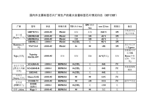
国内外主要电子标签芯片厂商生产的大容量标签芯片归总(RFID,HF&UHF)
无
1280
无
意联(Alien,美国)
Higgs 3
18000-6C
EEPROM
96
96
512
无
EM(瑞士)
EM4325
18000-6C
EEPROM
48
352
3072
SPI
EM4233
18000-3
EEPROM
64(UID)
无
2K
无
英飞凌(Infineon,德国)
SRF 55V10S
18000-3
18000-6C
未知
未知
224
4k*8(默认)
未知
容量最大可达32K Bytes(空客定制,不外售)
意法半导体(ST,意大利&法国)
M24LR64-R
18000-3
EEPROM
64(UID)
无
64K
I2C
M24LR64E-R
18000-3
EEPROM
64(UID)
无
64K
I2C
有能量搜集模块
LRIS64K
FRAM
256
560
4K*8
SPI
MB89R803A
18000-6C
FRAM
256
560
4K*8
无
MB89R112
18000-3
FRAM
64(UID)
无
9K*8
SPI
Ramtron(美国)
WM72016
18000-6C
FRAM
64
96
16K
SPI
该公司已并入Cypress
Tego(美国)
VHFUHF无线发射芯片RF2516的原理与应用解析

VHF/UHF无线发射芯片RF2516的原理与应用RF2516是RFMicroDevice公司推出的一种单片AM/ASKVHF/UHF发射芯片,可工作于100MHz~500MHz,并采用AM/ASK调制方式。
其片内集成了PLL、VCO和参考振荡器。
工作电压为2.25V~3.6V,可为50Ω负载提供±10dBm的输出功率。
RF2516可应用在315MHz~433MHz的远程无钥匙接入系统、无线安全系统及其它远程控制设备中。
由于其片内集成了VCO、鉴相器、预定标器和参考振荡器,因此,只要外接一个晶体谐振器就可构成完整的锁相环。
RF2516除了具有标准的掉电模式外,还具有自动锁相检测功能。
当PLL失锁时,发射输出无效.1引脚功能RF2516采用16脚QSOP封装形式。
下面是其各引脚的功能说明:脚1(OSCB):该脚直接和参考振荡器三极管的基极相连。
一个68pF的电容接在该脚和引脚2间;脚2(OSCE): 该脚直接和参考振荡器三极管的发射极相连。
一个33pF的电容接在该脚和地之间;脚3(PD):当该脚为低电平时,所有的电路关闭;当该脚为高电平时,电路正常工作;脚4(GND):TXOUT放大器的接地端,应使引线尽量短并直接连接到地,以求最佳的工作性能;脚5(TXOUT):发射输出端,该脚是集电极开路输出端,需要接一个馈电电感与匹配电容,构成集电极谐振匹配电路同时给放大器的集电极馈电;脚6(GND1):TX输出缓冲放大器接地端;脚7(VCC1):该脚给缓冲放大器提供偏置;脚8(MODIN):AM、数字调制信号通过该脚加给载波。
一个外部电阻通过该脚给输出放大器提供偏置,其电压不能超过1.1V,过高的电压可能损坏器件;脚9(VCC2):该脚用来给VCO、晶体振荡器、鉴相器提供直流偏置。
中频旁路电容应直接接在该脚和地之间;脚10(GND2):数字PLL接地端;脚11(VREFP):旁路偏置参考电压引脚,旁路电容应选择合适的大小以给参考晶体振荡器滤波,旁路电容直接和该脚相连;脚12(RESNTR-):该脚用来给VCO提供直流控制电压,并调节VCO的中心频率;脚13(RESNTR+):和引脚12相同;脚14(LOOPFLT):泵电路输出端,从该脚到地的RC网络用来设置PLL带宽;脚15(LDFLT):该脚用来设置锁定检测电路的门限,旁路电容用来和片内1kΩ电阻设置RC时间常数。
常用无线射频芯片

常用无线射频芯片目录CC1000PWR 超低功率射频收发器CC1010PAGR 射频收发器和微控制器CC1020RSSR 射频收发器CC1021RSSR 射频收发器CC1050PWR 超低功率射频发送器CC1070RSQR 射频发送器CC1100RTKR 多通道射频收发器CC1101RTKR 低于1GHz射频收发器CC1110F16RSPR 射频收发片上系统CC1110F32RSPR 射频收发片上系统CC1110F8RSPR 射频收发片上系统CC1111F16RSPR 射频收发片上系统CC1111F32RSPR 射频收发片上系统CC1111F8RSPR 射频收发片上系统CC1150RSTR 多通道射频发送器CC2400RSUR 多通道射频发送器CC2420RTCR 2.4GHz射频收发器CC2420ZRTCR 2.4GHz射频收发器CC2430F128RTCR ZigBee 芯片CC2430ZF128RTCR ZigBee 芯片CC2431RTCR 无线传感器网络芯片CC2431ZRTCR 无线传感器网络芯片CC2480A1RTCR 2.4GHzZigBee处理器CC2500RTKR 2.4GHz射频收发器CC2510F16RSPR 2.4GHz无线电收发器CC2510F32RSPR 2.4GHz无线电收发器CC2510F8RSPR 2.4GHz无线电收发器CC2511F16RSPR 2.4GHz无线电收发器CC2511F32RSPR 2.4GHz无线电收发器CC2511F8RSPR 2.4GHz无线电收发器CC2520RHDR 射频收发器CC2530F128RHAR 射频收发器CC2530F256RHAR 射频收发器CC2530F64RHAR 射频收发器CC2550RSTR 2.4GHz发送器CC2590RGVR 2.4GHz射频前端芯片CC2591RGVR 2.4GHz射频前端芯片CCZACC06A1RTCR 2.4GHZ ZigBee芯片TRF7900APWR 27MHz双路接收器TRF6900APT 射频收发器TRF6901PTG4 射频收发器TRF6901PTRG4 射频收发器TRF6903PTG4 射频收发器TRF6903PTRG4 射频收发器ADF7020-1BCPZ-RL7 射频收发IC ADF7020BCPZ-RL7 射频收发ICADF7021BCPZ-RL7 ISM无线收发IC ADF7021-NBCPZ-RL7 ISM无线收发IC ADF7025BCPZ-RL7 射频收发ICADF7010BRUZ-REEL7 ISM无线发射IC ADF7011BRUZ-RL7 ISM无线发射IC ADF7012BRUZ-RL7 UHF无线发射IC ADF7901BRUZ-RL7 ISM无线发射IC A7121A71C21AQF 2.4GHz射频收发器A7122A71C22AQF 2.4GHz射频收发器A7102A71C02AQF 射频收发ICA7103A71C03AUF 射频收发ICA7201A72C01AUF 射频接收ICA7202A72C02AUF 射频接收ICA7302A73C02AMF 射频发射ICA7105A71X05AQF 2.4GHz射频收发IC A7125A71X25AQF 2.4GHz射频收发IC A7325A73X25AQF 2.4GHz射频发射IC A7303AA73C03AQF FM发射芯片A7303AA73C03AUF FM发射芯片A7303BA73C03BUF FM发射芯片A7303BA73C03BQF FM发射芯片A7282A72N82AQF GPS接收芯片A7531BA75C31BQF GPS开关芯片A7532A75C32AQF GPS开关芯片A7533A75X33AQF GPS开关芯片A7533A75X33BQF GPS开关芯片AS3931 低功耗无线接收芯片AS3932BTSW 低功耗无线接收芯片AS3932BQFW 低功耗无线接收芯片AS3977BQFT FSK发射芯片AT86RF211DAI-R 射频收发ICAT86RF211SAHW-R 射频收发ICAT86RF212-ZU 射频收发ICAT86RF230-ZU 射频收发ICAT86RF231-ZU 射频收发ICATA2745M-TCQY 射频发送ICATA5428-PLQW 宽带收发ICATR2406-PNQG 2.4GHz射频收发IC T5750-6AQ 无线发射ICT5753-6AQ 无线发射ICT5754-6AQ 无线发射ICT7024-PGPM 前端收发器U2741B-NFB 无线发射ICAX5051 射频收发器ICAX5042 射频收发器ICAX5031 射频收发器ICAX50424 射频收发器ICAX6042 射频收发器ICCYRF6936-40LFXC 无线USB芯片CYRF7936-40LFXC 无线收发器芯片CYWUSB6932-28SEC 无线USB芯片CYWUSB6934-28SEC 无线USB芯片CYWUSB6934-48LFXC 无线USB芯片CYWUSB6935-28SEI 无线USB芯片CYWUSB6935-48LFI 无线USB芯片CYWUSB6935-48LFXC 无线USB芯片CYWUSB6935-48LFXI 无线USB芯片CYRF69103-40LFXC 无线射频芯片CYRF69213-40LFXC 无线射频芯片CYWUSB6953-48LFXC 无线USB芯片EM2420-RTR ZigBee 芯片EM260-RTR ZigBee 芯片EM250-RTR ZigBee 芯片EM351-RTR ZigBee 芯片EM357-RTR ZigBee 芯片PA5305 射频功率放大器PA2420 射频功率放大器PA2421 射频功率放大器PA2432 射频功率放大器FM2422 射频前端模块FM2422U 射频前端模块FM2427 射频前端模块FM2429 射频前端模块FM2429U 射频前端模块FM2446 射频前端模块FM7705 射频前端模块FM7707 射频前端模块MC13190FCR2 射频收发ICMC13191FCR2 射频收发ICMC13192FCR2 射频收发ICMC13193FCR2 射频收发ICMC13201FCR2 射频收发ICMC13202FCR2 射频收发ICMC13203FCR2 射频收发ICMC13211R2 射频收发ICMC13212R2 射频收发ICMC13213R2 射频收发ICMC13214R2 射频收发ICMC13224V 802.15.4/ZigBee芯片TDA5200 ASK接收器TDA5201 ASK接收器TDA5210 ASK/FSK接收器TDA5211 ASK/FSK接收器TDA5212 ASK/FSK接收器TDA5220 ASK/FSK接收器TDA5221 ASK/FSK接收器TDA7200 ASK/FSK接收器TDA7210 ASK/FSK接收器TDA5230 ASK/FSK接收器TDA5231 ASK/FSK接收器TDK5100 ASK/FSK发射器TDK5100F ASK/FSK发射器TDK5101 ASK/FSK发射器TDK5101F ASK/FSK发射器TDK5102 ASK/FSK发射器TDK5103A ASK发射器TDK5110 ASK/FSK发射器TDK5110F ASK/FSK发射器TDK5111 ASK/FSK发射器TDK5111F ASK/FSK发射器TDA7116F ASK/FSK发射器PMA7105 ASK/FSK发射器PMA7106 ASK/FSK发射器PMA7107 ASK/FSK发射器PMA7110 ASK/FSK发射器TDA5250 ASK/FSK收发器TDA5251 ASK/FSK收发器TDA5252 ASK/FSK收发器TDA5255 ASK/FSK收发器MAX1470EUI+T 无线接收IC MAX1471ATJ+T 无线接收IC MAX1472AKA+T 无线发射IC MAX1473EUI+T 无线接收IC MAX1479ATE+T 无线发射IC MAX7030HATJ+T 无线收发IC MAX7030LATJ+T 无线收发IC MAX7031LATJ+T 无线收发IC MAX7031MATJ50+T 无线收发ICMAX7032ATJ+T 无线收发IC MAX7033ETJ+T 无线接收IC MAX7044AKA+T 无线发射IC MAX7058ATG+T 无线发射IC MLX71121ELQ 射频接收IC MLX71122ELQ 射频接收IC TH71071EDC 射频接收IC TH71072EDC 射频接收IC TH7107EFC 射频接收IC TH71081EDC 射频接收IC TH71082EDC 射频接收IC TH7108EFC 射频接收IC TH71101ENE 射频接收IC TH71102ENE 射频接收IC TH71111ENE 射频接收IC TH71112ENE 射频接收IC TH71221ELQ 射频接收IC TH7122ENE 射频收发IC TH72001KDC 射频发射IC TH72002KDC 射频发射IC TH72005KLD 射频发射IC TH72006KLD 射频发射IC TH72011KDC 射频发射IC TH72012KDC 射频发射IC TH72015KLD 射频发射IC TH72016KLD 射频发射IC TH72031KDC 射频发射IC TH72032KDC 射频发射IC TH72035KLD 射频发射IC TH72036KLD 射频发射IC MICRF102BM 无线发射IC MICRF112YMM 无线发射IC MICRF113YM6 无线发射IC MICRF302YML 射频编码器MICRF405YML 射频发射IC MICRF505BML 射频收发IC MICRF506BML 射频收发IC MICRF002YM 射频接收器MICRF005YM 无线接收IC MICRF007BM UHF接收器MICRF008BM 无线接收IC MICRF009BM UHF接收IC MICRF010BM UHF接收IC MICRF011BM 射频ICMICRF211AYQS 射频接收器MRF24J40-I/ML ZigBee芯片MRF24J40T-I/ML ZigBee芯片MCP2030-I/P 免钥登录芯片MCP2030-I/SL 免钥登录芯片MCP2030-I/ST 免钥登录芯片MCP2030T-I/SL 免钥登录芯片MCP2030T-I/ST 免钥登录芯片nRF2401AG 2.4GHz收发器IC nRF24AP1 2.4GHz收发器IC nRF24E1G 2.4GHz收发器IC nRF24E2G 2.4GHz发射器IC nRF24L01+ 2.4GHz收发器IC nRF24LE1 2.4GHz收发器IC nRF24LU1 2.4GHz收发器IC nRF24Z1 2.4GHz收发器ICNRF905 430 928MHz收发器NRF9E5 430-928MHz收发器MFRC50001T/0FE,112 阅读器IC MFRC53001T/0FE,112 阅读器IC MFRC53101T/0FE,112 阅读器IC MFRC52301HN1 阅读器ICPN5110A0HN1/C2 收发器ICPN5120A0HN1/C1 收发器ICPN5310A3HN/C203 NFC控制器IC PN1000 GPS RF接收ICRX3400 射频接收ICRX3930 射频接收ICRX3140 射频接收ICRX3310A 射频接收ICRX3361 射频接收ICRX3408 射频接收ICPT4301 射频接收ICPT4316 射频接收ICPT4450 射频发射ICTX4915 射频发射ICTX4930 射频发射ICPA2460 功率放大器ICPA2464 功率放大器ICFS8107E 锁相环ICFS8108 锁相环ICFS8160 锁相环ICFS8170 锁相环ICFS8308 锁相环ICMG2400-F48 ZigBee单芯片MG2450-B72 ZigBee单芯片MG2455-F48 ZigBee单芯片AP1092 功率放大器ICAP1098 功率放大器ICAP1110 功率放大器ICAP1091 功率放大器ICAP1093 功率放大器ICAP1280 PA/LNA功率放大器AP1213 射频前端模块AP1290 功率放大器ICAP1291 功率放大器ICAP1294 功率放大器ICAP1045 功率放大器ICAP1046 功率放大器ICAP2085 功率放大器ICAP2010C 功率放大器ICAP3011 功率放大器ICAP3013 功率放大器ICAP3014 功率放大器ICAP3015 功率放大器ICAP3211 功率放大器ICSX1211I084TRT 单芯片收发器SX1441I077TRLF 系统蓝牙芯片XE1203FI063TRLF 射频收发芯片XE1205I074TRLF 射频收发芯片XE1283I076TRLF 射频收发芯片XM1203FC433XE1 射频收发芯片XM1203FC868XE1 射频收发芯片XM1203FC915XE1 射频收发芯片SX1223I073TRT 射频发射芯片SI3400-E1-GM 以太网电源ICSI3401-E1-GM 以太网电源ICSI3460-D01-GM 以太网电源ICSI4020-I1-FT 射频发射ICSI4021-A1-FT 射频发射ICSI4022-A1-FT 射频发射ICSI4030-A0-FM 射频发射ICSI4031-A0-FM 射频发射ICSI4032-V2-FM 射频发射ICSi4230-A0-FMIA4230 无线发射IC Si4231-A0-FMIA4231 无线发射IC Si4232-A0-FMIA4232 无线发射IC Si4320-J1-FT 无线接收ICSi4322-A1-FT 无线接收ICSi4330-V2-FMIA4330 无线接收IC SI4420-D1-FT 射频收发ICSI4421-A1-FTIA4421 无线收发IC SI4430-A0-FMIA4430 无线收发IC SI4431-A0-FMIA4431 无线收发IC SI4432-V2-FMIA4432 无线收发IC TM1001 功率放大器ICTM1006 功率放大器ICTM1008 射频晶体管TM3001 射频开关ICTM3002 射频开关ICTM4001 FM发射ICUW2453 无线网络ICUZ2400 ZigBee 芯片UP2206 2.4GHz功率放大器UP2268 2.4GHz功率放大器UA2707 射频信号放大器UA2709 射频信号放大器UA2711 射频信号放大器UA2712 射频信号放大器UA2715 射频信号放大器UA2716 射频信号放大器UA2725 射频信号放大器UA2731 射频信号放大器UA2732 射频信号放大器W2805 无线视频ICW2801 无线音频IC。
CC1101 射频的UHF收发器解析

CC1101在CC1100主要改善部分改善杂散响应;更紧密的相位噪声更好的改善邻道功率(ACP )的性能;饱和电平输入更高;更高效能的功率输出连续频率波段的扩展,CC1100: 400-464 MHz 和800-928 MHzCC1101: 387-464 MHz 和779-928 MHz产品简介CC1100/CC1101是Chipcon(已被TI收购)推出的一款低成本单片射频的UHF收发器。
该芯片电路主要设定为在315、433、868和915MHz 的ISM(工业,科学和医学),集成了一个软件可编程的调制解调器。
该调制解调器支持2-FSK、GFSK和MSK调制格式,数据传输率最高可达500kbps。
通过开启集成在调制解调器上的前向误差校正选项,能使性能得到提升。
CC1100/CC1101硬件支持数据包处理、数据缓冲、突发数据传输、清晰信道评估、连接质量指示和电磁波激发MCU可以通过SPI 接口与CC1100进行命令和数据交换。
CC1100/CC1101主要应用于低功耗无线应用设计。
CC1101在CC1100基础上主要进行以下改进改善杂散响应,饱和电平输入更高;连续频率波段的扩展:CC1100: 400-464 MHz和800-928 MHz;CC1101: 387-464 MHz和779-928 MHz;CC1101和CC1100二者在软件编程上完全兼容;更高效能的功率输出,能量越集中,信号传输就越远;更紧密的相位噪声更好的改善邻道功率(ACP)的性能,改善了近距离信号堵塞现象。
虽然CC1100芯片还存在,但鉴于CC1101的改进特性,我公司研制的模块已经从09年开始全部采用CC1101芯片。
为便于用户开发,我们提供配套评估套件,为产品开发保驾护航,使无线应用开发大大加速,并避免不必要的误区。
基本特点工作电压:1.8-3.6V工作频率:(模块:387-464MHZ)瞬间最大工作电流: <30mA;最大发射功率: 10mW (+10dBm);315/433/868/915MHZ的ISM频段;支持2-FSK、GFSK和MSK调制方式;接收灵敏度在1200波特率下-110dBm;最低工作速率1.2kbps,最高500kbps;单独的64字节RX和TX数据FIFO缓冲区;内置硬件CRC 检错可确保数据可靠传输;支持RSSI强弱信号检测和载波侦听功能;功耗低(RX中,15.6mA,2.4kbps,433MHz;快速频率变动合成器带来的合适的频率跳跃系统;通信地址(256个)工作频率都可以通过SPI编程设置;可编程控制的输出功率,对所有的支持频率可达+10dBm;WOR功能可设置待机、接收状态定时切换时间比例以降低功耗;典型主要应用车辆监控、遥控、遥测、水文气象监控无线标签、身份识别、非接触RF智能卡小型无线网络、无线抄表、门禁系统、小区传呼工业数据采集系统、无线232数据通信、无线485/422数据通信无线数据终端、安全防火系统、无线遥控系统、生参考例程更多功率参数设置可详细参考DATACC1101英文文档中第48-49页的参数表//INT8U PaTabel[8] ={0x04 ,0x04 ,0x04 ,0x04 ,0x04 ,0x04 ,0x04 ,0x04}; //-30dBm 功率最小//INT8U PaTabel[8] = {0x60 ,0x60 ,0x60 ,0x60 ,0x60 ,0x60 ,0x60 ,0x60};//0dBmINT8U PaTabel[8] ={0xC0 ,0xC0 ,0xC0 ,0xC0 ,0xC0 ,0xC0 ,0xC0 ,0xC0}; //10dBm 功率最大SPI读写操作INT8U SpiTxRxByte(INT8U dat){INT8U i,temp;temp = 0;SCK = 0;for(i=0; i<8; i++){if(dat & 0x80){MOSI = 1;}else MOSI = 0;dat <<= 1;SCK = 1;_nop_();_nop_();temp <<= 1;if(MISO)temp++;SCK = 0;_nop_();_nop_();}return temp;}SPI写寄存器操作void halSpiWriteReg(INT8U addr, INT8U value) {CSN = 0;while (MISO);SpiTxRxByte(addr); //写地址SpiTxRxByte(value); //写入配置CSN = 1;}SPI读寄存器操作INT8U halSpiReadReg(INT8U addr){INT8U temp, value;temp = addr|READ_SINGLE;//读寄存器命令CSN = 0;while (MISO);SpiTxRxByte(temp);value = SpiTxRxByte(0);CSN = 1;return value;}CC1101初始化设置RF_SETTINGS rfSettings ={0x00,0x08, // FSCTRL1 Frequency synthesizer control.0x00, // FSCTRL0 Frequency synthesizer control.0x10, // FREQ2 Frequency control word, high byte.0xA7, // FREQ1 Frequency control word, middle byte.0x62, // FREQ0 Frequency control word, low byte.0x5B, // MDMCFG4 Modem configuration.0xF8, // MDMCFG3 Modem configuration.0x03, // MDMCFG2 Modem configuration.0x22, // MDMCFG1 Modem configuration.0xF8, // MDMCFG0 Modem configuration.0x00, // CHANNR Channel number.0x47, // DEVIATN Modem deviation setting0xB6, // FREND1 Front end RX configuration.0x10, // FREND0 Front end RX configuration.0x18, // MCSM0 Main Radio Control State Machine configuration.0x1D, // FOCCFG Frequency Offset Compensation Configuration.0x1C, // BSCFG Bit synchronization Configuration.0xC7, // AGCCTRL2 AGC control.0x00, // AGCCTRL1 AGC control.0xB2, // AGCCTRL0 AGC control.0xEA, // FSCAL3 Frequency synthesizer calibration.0x2A, // FSCAL2 Frequency synthesizer calibration.0x00, // FSCAL1 Frequency synthesizer calibration.0x11, // FSCAL0 Frequency synthesizer calibration.0x59, // FSTEST Frequency synthesizer calibration.0x81, // TEST2 Various test settings.0x35, // TEST1 Various test settings.0x09, // TEST0 Various test settings.0x0B, // IOCFG2 GDO2 output pin configuration.0x06, // IOCFG0D GDO0 output pin configuration.0x04, // PKTCTRL1 Packet automation control.0x05, // PKTCTRL0 Packet automation control.0x00, // ADDR Device address.0x0c // PKTLEN Packet length.};数据接收流程操作INT8U halRfReceivePacket(INT8U *rxBuffer, INT8U *length){INT8U status[2];INT8U packetLength;INT8U i=(*length)*4; //具体多少要根据datarate和length来决定halSpiStrobe(CCxxx0_SRX); //进入接收状态delay(2);while (GDO0){delay(2);--i;if(i<1)return 0;}if ((halSpiReadStatus(CCxxx0_RXBYTES) & BYTES_IN_RXFIFO))//如果接的字节数不为0{packetLength = halSpiReadReg(CCxxx0_RXFIFO);//读出第一个字节,此字节为该帧数据长度if (packetLength <= *length)//如果所要的有效数据长度小于等于接收到的数据包的长度{halSpiReadBurstReg(CCxxx0_RXFIFO, rxBuffer, packetLength);//读出所有接收到的数据*length =packetLength;//把接收数据长度的修改为当前数据的长度// Read the 2 appended status bytes (status[0] = RSSI, status[1] = LQI)halSpiReadBurstReg(CCxxx0_RXFIFO, status, 2);//读出CRC校验位halSpiStrobe(CCxxx0_SFRX); //清洗接收缓冲区return (status[1] & CRC_OK); //如果校验成功返回接收成功}else{*length = packetLength;halSpiStrobe(CCxxx0_SFRX); //清洗接收缓冲区return 0;}}elsereturn 0;}数据发送流程操作void halRfSendPacket(INT8U *txBuffer, INT8U size){halSpiWriteReg(CCxxx0_TXFIFO, size);halSpiWriteBurstReg(CCxxx0_TXFIFO, txBuffer, size);//写入要发送的数据halSpiStrobe(CCxxx0_STX); //进入发送模式发送数据// Wait for GDO0 to be set -> sync transmittedwhile (!GDO0);// Wait for GDO0 to be cleared -> end of packetwhile (GDO0);halSpiStrobe(CCxxx0_SFTX);}无线应用注意事项(1)无线模块的VCC电压范围为1.8V-3.6V之间,不能在这个区间之外,超过3.6V将会烧毁模块。
UHF频段无线影音发射器
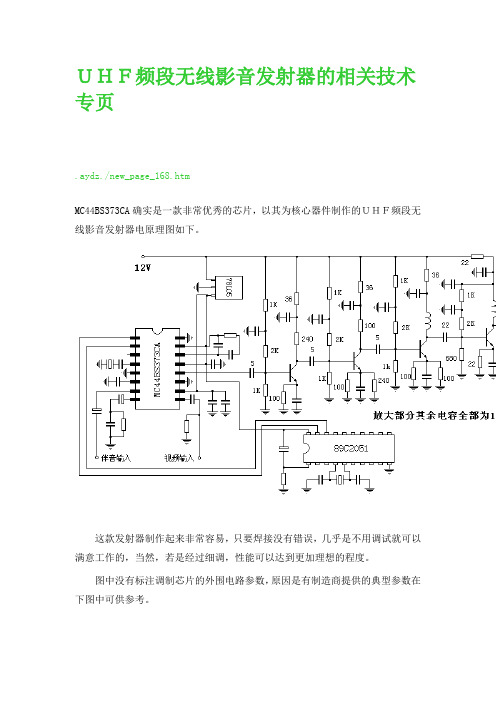
UHF频段无线影音发射器的相关技术专页.aydz./new_page_168.htmMC44BS373CA确实是一款非常优秀的芯片,以其为核心器件制作的UHF频段无线影音发射器电原理图如下。
这款发射器制作起来非常容易,只要焊接没有错误,几乎是不用调试就可以满意工作的,当然,若是经过细调,性能可以达到更加理想的程度。
图中没有标注调制芯片的外围电路参数,原因是有制造商提供的典型参数在下图中可供参考。
调制芯片的工作状态用单片机来控制非常方便,这里选取常用的89C2051芯片,随处可以买到,引脚功能如下图所示。
用于控制调制芯片的程序根据自己的需要可简可繁。
假如您是单片机高手,此程序可参考调制芯片制造商提供的资料自行设计;假如您嫌费事儿,或者您对单片机编程不是十分精通,可以到论坛上选择适合您用的现成程序;假如您对单片机编程一无所知,也没关系,这里提供网友《cyy》设计的一个软件,可以自动生成HEX格式文件,直接写入单片机即可。
假如您对单片机的使用不太了解,或者手头没有可用来对单片机写入数据的编程器,我们也可以免费代劳,提供写好程序的单片机芯片,插入即可工作。
89C2051芯片5元/片,另加《中国邮政》普件邮费每次5元。
网友《cyy》设计的BS373控制程序生成器软件点击下载MC44BS373CA芯片制造商提供的技术资料点击下载假如您对单片机一无所知,那也没关系,照着下面介绍的方法操作也能解决问题。
第一步,下载这里推荐的单片机程序生成软件,解压安装运行,出现下面的界面。
此界面一目了然,我想,能走到这一步的朋友都应该能够看明白的,不然,您可能下载解压安装软件时早就遇到困难了,那就只能先熟悉一下计算机的使用常识了。
按“生成目标hex文件”按钮,将文件保存到您自己认为方便的地方备用。
第二步,找到能够往单片机里写入程序(就是刚才生成的那个文件)的设施。
我们目前用的是好朋友刚推荐的《TOP2004通用USB编程器》,他的上对各种编程器的安装和使用有非常详尽的描述,同时供应各种编程器,我们就不在这里赘述了。
UHF(远望谷)与HF(3M等)的对比说明1

目前国内外已经安装了射频识别工程的领域有物流、零售、出版、图书馆、医疗、制造、 教育、政府和公用服务、生活消费品、国防、海运、运输和家畜养殖。其中,对物流和图书 馆领域的追踪表明,这两个领域是射频识别使用率最高的领域。从 2006 年起,随着更多的 企业采用射频识别,UHF 标签将主导射频识别市场,UHF 射频标签识别技术是未来物流识别 特别是海量物品盘点的主流。
宁波市远望谷
2
invengo
UHF 与 HF 对比说明
国家(地区) 美国/加拿大 欧盟(英法德意荷等国)
中国 中国香港特别行政区
中国台湾省 新加坡 日本 韩国 印度
澳大利亚 新西兰
划定情况 已划定 已划定 已划定 已划定 已划定 已划定 已划定 已划定 已划定 已划定 已划定
UHF 分配频段 902-928MHz 865.6-867.6MHz 840-845MHz/920-925MHz 865-868MHz/920-925MHz 922-928MHz 866-869MHz/920-925MHz 950-956MHz 908.5-914MHz 865-867MHz 920-926MHz 864-868MHz
电耦合
电磁场反向散射耦合
迟钝----------------------敏感
大-------------------------小
近-------------------------远
低速----------------------高速
宁波市远望谷
3
invengo
UHF 与 HF 对比说明
RFID 系统主要用途及特点
二.UHF 与 HF 对比介绍
RFID 典型的工作频率有:125KHz、13.56MHz、902MHz~928MHz、2.45GHz 等。其 中 125kHz 与 13.56MHz 两个频段应用的区域相对集中,称为低频和高频。超高频的典型工 作频率主要集中在 902MHz~928MHz。