L2722,L2720,L2724, 规格书,Datasheet 资料
二七二一型号LED指示灯技术数据表说明书

27-21/GHC-YR1S2M/3C
Pb EVERLIGHT
CPN : P N: XXXXXXXXXXXXX
XXXXXXXXXXXXX QTY : XXX
LOT NO : XXXXXXXXXX
RoHS
CAT : XXX HUE : XXX REF : XXX
Reference : XXXXXXXX
Parameter
Symbol Min. Typ.
Luminous Intensity
IV
112
-----
Viewing Angle
2θ1/2 ----
130
Peak Wavelength
λp
----
518
Dominant Wavelength
λd
520
-----
Spectrum Radiation
3.Tolerance of Forward Voltage ±0.1V
Max. 285 ------535 ---3.95 50
Unit Condition
mcd
deg
nm IF=20mA
nm
nm V
μA
VR=5V
Everlight Electronics Co., Ltd. Device No:DSE-0001729
Label
Aluminum moisture-proof bag
Desiccant
Label
Everlight Electronics Co., Ltd. Device No:DSE-0001729
Prepared date: 12-Jun-2009
solder process. ․Mono-color type. ․Pb free ․The product itself will remain within RoHS compliant version
ALD2724SBL,ALD2724PBL,ALD2724ESBL,ALD2724EPBL, 规格书,Datasheet 资料
GENERAL DESCRIPTION The ALD2724E/ALD2724 is a dual monolithic operational amplifier with MOSFET input that has rail-to-rail input and output voltage ranges. The input voltage range and output voltage range are very close to the positive and negative power supply voltages. Typically the input voltage can be beyond positive power supply voltage V+ or the negative power supply voltage V- by up to 300mV. The output voltage swings to within 60mV of either positive or negative power supply voltages at rated load. With high impedance load, the output voltage of the ALD2724E/ALD2724 approaches within 1mV of the power supply rails. This device is designed as an alternative to the popular J-FET input operational amplifier in applications where lower operating voltages, such as 9V battery or ±3.25V to ±5V power supplies are being used. The ALD2724E/ALD2724 offers high slew rate of 5.0V/µs. The rail-to-rail input and output feature of the ALD2724E/ALD2724 expands signal voltage range for a given operating supply voltage and allows numerous analog serial stages to be implemented without losing operating voltage margin. The output stage is designed to drive up to 10mA into 400pF capacitive and 1.5KΩ resistive loads at unity gain and up to 4000pF at a gain of 5. Short circuit protection to either ground or the power supply rails is at approximately 15mA clamp current. Due to complementary output stage design, the output can source and sink 10mA into a load with symmetrical drive and is ideally suited for applications where push-pull voltage drive is desired.
LM2742资料
LM2742N-Channel FET Synchronous Buck Regulator Controller for Low Output VoltagesGeneral DescriptionThe LM2742is a high-speed,synchronous,switching regu-lator controller.It is intended to control currents of 0.7A to 20A with up to 95%conversion efficiencies.Power up and down sequencing is achieved with the power-good flag,adjustable soft-start and output enable features.The LM2742operates from a low-current 5V bias and can con-vert from a 1V to 16V power rail.The part utilizes a fixed-frequency,voltage-mode,PWM control architecture and the switching frequency is adjustable from 50kHz to 2MHz by setting the value of an external resistor.Current limit is achieved by monitoring the voltage drop across the on-resistance of the low-side MOSFET,which enables on-times on the order of 40ns,one of the best in the industry.The wide range of operating frequencies gives the power supply de-signer the flexibility to fine-tune component size,cost,noise and efficiency.The adaptive,non-overlapping MOSFET gate-drivers and high-side bootstrap structure helps to fur-ther maximize efficiency.The high-side power FET drain voltage can be from 1V to 16V and the output voltage is adjustable down to 0.6V.Featuresn Input power from 1V to 16Vn Output voltage adjustable down to 0.6Vn Power Good flag,adjustable soft-start and output enable for easy power sequencingn Reference Accuracy:1.5%(0˚C -125˚C)n Current limit without sense resistor n Soft startn Switching frequency from 50kHz to 2MHz n 40ns typical minimum on-time n TSSOP-14packageApplicationsn POL power supply modules n Cable Modemsn Set-Top Boxes/Home Gateways n DDR Core Powern High-Efficiency Distributed Power nLocal Regulation of Core PowerTypical Application20087510PRELIMINARYMarch 2004LM2742N-Channel FET Synchronous Buck Regulator Controller for Low Output Voltages©2004National Semiconductor Corporation Connection Diagram2008751114-Lead Plastic TSSOPθJA =155˚C/WNS Package Number MTC14Pin DescriptionBOOT (Pin 1)-Supply rail for the N-channel MOSFET gate drive.The voltage should be at least one gate threshold above the regulator input voltage to properly turn on the high-side N-FET.LG (Pin 2)-Gate drive for the low-side N-channel MOSFET.This signal is interlocked with HG to avoid shoot-through problems.PGND (Pins 3,13)-Ground for FET drive circuitry.It should be connected to system ground.SGND (Pin 4)-Ground for signal level circuitry.It should be connected to system ground.V CC (Pin 5)-Supply rail for the controller.PWGD (Pin 6)-Power Good.This is an open drain output.The pin is pulled low when the chip is in UVP ,OVP ,or UVLO mode.During normal operation,this pin is connected to V CC or other voltage source through a pull-up resistor.ISEN (Pin 7)-Current limit threshold setting.This sources a fixed 50µA current.A resistor of appropriate value should be connected between this pin and the drain of the low-side FET.EAO (Pin 8)-Output of the error amplifier.The voltage level on this pin is compared with an internally generated ramp signal to determine the duty cycle.This pin is necessary for compensating the control loop.SS (Pin 9)-Soft start pin.A capacitor connected between this pin and ground sets the speed at which the output voltage ramps rger capacitor value results in slower output voltage ramp but also lower inrush current.FB (Pin 10)-This is the inverting input of the error amplifier,which is used for sensing the output voltage and compen-sating the control loop.FREQ (Pin 11)-The switching frequency is set by connect-ing a resistor between this pin and ground.SD (Pin 12)-IC Logic Shutdown.When this pin is pulled low the chip turns off both the high side and low side switches.While this pin is low,the IC will not start up.An internal 20µA pull-up connects this pin to V CC .For a device which turns on the low side switch during shutdown,see the pin compatible LM2737.HG (Pin 14)-Gate drive for the high-side N-channel MOS-FET.This signal is interlocked with LG to avoid shoot-through problems.L M 2742 2Absolute Maximum Ratings(Note1)If Military/Aerospace specified devices are required, please contact the National Semiconductor Sales Office/ Distributors for availability and specifications.V CC7V BOOTV21V LG and HG to GND(Note3)-2V to21V Junction Temperature150˚C Storage Temperature−65˚C to150˚C Soldering InformationLead Temperature(soldering,10sec)260˚C Infrared or Convection(20sec)235˚C ESD Rating2kVOperating RatingsSupply Voltage(V CC) 4.5V to5.5V Junction Temperature Range−40˚C to+125˚C Thermal Resistance(θJA)155˚C/WElectrical CharacteristicsV CC=5V unless otherwise indicated.Typicals and limits appearing in plain type apply for T A=T J=+25˚C.Limits appearing in boldface type apply over full Operating Temperature Range.Datasheet min/max specification limits are guaranteed by design, test,or statistical analysis.Symbol Parameter Conditions Min Typ Max UnitsV FB_ADJ FB Pin Voltage V CC=4.5V,0˚C to+125˚C0.5910.60.609V V CC=5V,0˚C to+125˚C0.5910.60.609V CC=5.5V,0˚C to+125˚C0.5910.60.609V CC=4.5V,−40˚C to+125˚C0.5890.60.609V CC=5V,−40˚C to+125˚C0.5890.60.609V CC=5.5V,−40˚C to+125˚C0.5890.60.609V ON UVLO Thresholds RisingFalling 4.23.6VI Q-V5Operating V CC CurrentSD=5V,FB=0.55VFsw=600kHz1 1.52mASD=5V,FB=0.65VFsw=600kHz0.8 1.7 2.2 Shutdown V CC Current SD=0V0.150.40.7mAt PWGD1PWGD Pin Response Time FB Voltage Going Up6µs t PWGD2PWGD Pin Response Time FB Voltage Going Down6µs I SD SD Pin Internal Pull-up Current20µA I SS-ON SS Pin Source Current SS Voltage=2.5V0˚C to+125˚C -40˚C to+125˚C 8511111515µAI SS-OC SS Pin Sink Current During OverCurrent SS Voltage=2.5V95µAI SEN-TH I SEN Pin Source Current TripPoint0˚C to+125˚C-40˚C to+125˚C352850506565µAERROR AMPLIFIERGBW Error Amplifier Unity GainBandwidth5MHzG Error Amplifier DC Gain60dBSR Error Amplifier Slew Rate6V/µAI FB FB Pin Bias Current FB=0.55VFB=0.65V 01530100155nAI EAO EAO Pin Current Sourcing andSinking V EAO=2.5,FB=0.55VV EAO=2.5,FB=0.65V2.80.8mAV EA Error Amplifier Maximum Swing MinimumMaximum1.23.2VLM27423Electrical Characteristics(Continued)V CC =5V unless otherwise indicated.Typicals and limits appearing in plain type apply for T A =T J =+25˚C.Limits appearing in boldface type apply over full Operating Temperature Range.Datasheet min/max specification limits are guaranteed by design,test,or statistical analysis.SymbolParameterConditionsMinTypMaxUnitsGATE DRIVE I Q-BOOTBOOT Pin Quiescent CurrentBOOT =12V,EN =00˚C to +125˚C -40˚C to +125˚C 9595160215µAR DS1Top FET Driver Pull-Up ON resistanceBOOT-SW =5V @350mA 3ΩR DS2Top FET Driver Pull-Down ON resistanceBOOT-SW =5V @350mA 2ΩR DS3Bottom FET Driver Pull-Up ON resistanceBOOT-SW =5V @350mA 3ΩR DS4Bottom FET Driver Pull-Down ON resistanceBOOT-SW =5V @350mA2ΩOSCILLATORf OSCPWM FrequencyR FADJ =590k Ω50kHzR FADJ =88.7k Ω300R FADJ =42.2k Ω,0˚C to +125˚C 500600700R FADJ =42.2k Ω,-40˚C to +125˚C 490600700R FADJ =17.4k Ω1400R FADJ =11.3k Ω2000D Max Duty Cycle f PWM =300kHz f PWM =600kHz9088%t on-min Minimum on-time40ns LOGIC INPUTS AND OUTPUTSV SD-IH SD Pin Logic High Trip Point 2.6 3.5V V SD-IL SD Pin Logic Low Trip Point 0˚C to +125˚C -40˚C to +125˚C 1.31.25 1.61.6VV PWGD-TH-LOPWGD Pin Trip PointsFB Voltage Going Down 0˚C to +125˚C -40˚C to +125˚C 0.4130.4100.4300.4300.4460.446VV PWGD-TH-HIPWGD Pin Trip PointsFB Voltage Going Up 0˚C to +125˚C -40˚C to +125˚C0.6910.6880.7100.7100.7340.734VV PWGD-HYSPWGD HysteresisFB Voltage Going Down FB Voltage Going Up35110mVNote 1:Absolute maximum ratings indicate limits beyond which damage to the device may occur.Operating ratings indicate conditions for which the device operates correctly.Opearting Ratings do not imply guaranteed performance limits.Note 2:The human body model is a 100pF capacitor discharged through a 1.5k resistor into each pin.Note 3:The LG and HG pin can have -2V to -0.5V applied for a maximum duty cycle of 10%with a maximum period of 1second.There is no duty cycle or maximum period limitation for a LG and HG pin voltage range of -0.5V to 21V.L M 2742 4Typical Performance CharacteristicsEfficiency (V O =1.5V)F SW =300kHz,T A =25˚CEfficiency (V O =3.3V)F SW =300kHz,T A =25˚C2008751220087513V CC Operating Current vs TemperatureF SW =600kHz,No-Load Bootpin Current vs Temperature for BOOTV =12VF SW =600kHz,Si4826DY FET,No-Load2008751420087515Bootpin Current vs Temperature with 5V BootstrapF SW =600kHz,Si4826DY FET,No-Load PWM Frequency vs Temperaturefor R FADJ =43.2k Ω2008751620087517LM27425Typical Performance Characteristics(Continued)R FADJ vs PWM Frequency(in 100to 800kHz range),T A =25˚CR FADJ vs PWM Frequency(in 900to 2000kHz range),T A =25˚C2008751820087519V CC Operating Current Plus Boot Current vs PWM Frequency (Si4826DY FET,T A =25˚C)Switch Waveforms (HG Falling)V IN =5V,V O =1.8V I O =3A,C SS =10nF F SW =600kHz2008752020087523Switch Waveforms (HG Rising)V IN =5V,V O =1.8V I O =3A,F SW =600kHzStart-Up (No-Load)V IN =10V,V O =1.2V C SS =10nF,F SW =300kHz2008752420087521L M 2742 6Typical Performance Characteristics(Continued)Start-Up(Full-Load)V IN=10V,V O=1.2V I O=10A,C SS=10nFF SW=300kHzStart Up(No-Load,10x C SS)V IN=10V,V O=1.2VC SS=100nF,F SW=300kHz 2008752220087526Start Up(Full Load,10x C SS) V IN=10V,V O=1.2VI O=10A,C SS=100nFF SW=300kHzStart Up(Into1.2V Pre-Bias)V IN=12V,V O=2.5VNo Load,No Soft Start CapacitorF SW=300kHz2008752520087548Start Up(Into1.2V Pre-Bias) V IN=12V,V O=2.5VNo Load,C SS=10nFF SW=300kHzShutdownV IN=12V,V O=1.2VI O=10A,C SS=10nFF SW=300kHz2008754920087527LM2742 7Typical Performance Characteristics(Continued)Shutdown (No Load)V IN =12V,V O =1.2V I O =10A,C SS =10nFF SW =300kHzLoad Transient Response (I O =0to 4A)V IN =12V,V O =1.2VF SW =300kHz2008753320087528Load Transient Response (I O =4to 0A)V IN =12V,V O =1.2VF SW =300kHz Line Transient Response (V IN =5V to 12V)V O =1.2V,I O =5A F SW =300kHz2008752920087530Line Transient Response (V IN =12V to 5V)V O =1.2V,I O =5A F SW =300kHz Line Transient ResponseV O =1.2V,I O =5A F SW =300kHz2008753120087532L M 2742 8Block Diagram20087501Application InformationTHEORY OF OPERATIONThe LM2742is a voltage-mode,high-speed synchronous buck regulator with a PWM control scheme.It is designed for use in set-top boxes,thin clients,DSL/Cable modems,and other applications that require high efficiency buck convert-ers.It has power good (PWRGD),and output shutdown (SD).Current limit is achieved by sensing the voltage V DS across the low side FET.During current limit the high side gate is turned off and the low side gate turned on.The soft start capacitor is discharged by a 95µA source (reducing the maximum duty cycle)until the current is under control.START UPWhen V CC exceeds 4.2V and the shutdown pin SD sees a logic high the soft start capacitor begins charging through an internal fixed 10µA source.During this time the output of the error amplifier is allowed to rise with the voltage of the soft start capacitor.This capacitor,C SS ,determines soft start time,and can be determined approximately by:An application for a microprocessor might need a delay of 3ms,in which case C SS would be 12nF.For a different device,a 100ms delay might be more appropriate,in whichcase C SS would be 400nF.(39010%)During soft start the PWRGD flag is forced low and is released when the voltage reaches a set value.At this point this chip enters normal operation mode and the Power Good flag is released.Since the output is floating when the LM2742is turned off,it is possible that the output capacitor may be precharged to some positive value.During start-up,the LM2742operates fully synchronous and will discharge the output capacitor to some extent depending on the output voltage,soft start capacitance,and the size of the output capacitor.NORMAL OPERATIONWhile in normal operation mode,the LM2742regulates the output voltage by controlling the duty cycle of the high side and low side FETs.The equation governing output voltage is:V O =0.6x (R FB1+R FB2)/R FB1The PWM frequency is adjustable between 50kHz and 2MHz and is set by an external resistor,R FADJ ,between the FREQ pin and ground.The resistance needed for a desired frequency is approximately:LM27429Application Information(Continued)MOSFET GATE DRIVERSThe LM2742has two gate drivers designed for driving N-channel MOSFETs in a synchronous mode.Power for the drivers is supplied through the BOOT pin.For the high side gate (HG)to fully turn on the top FET,the BOOT voltage must be at least one V GS(th)greater than Vin.(BOOT ≥2*Vin)This voltage can be supplied by a separate,higher voltage source,or supplied from a local charge pump struc-ture.In a system such as a desktop computer,both 5V and 12V are usually available.Hence if Vin was 5V,the 12V supply could be used for BOOT.12V is more than 2*Vin,so the HG would operate correctly.For a BOOT of 12V,the initial gate charging current is 2A,and the initial gate dis-charging current is typically 6A.In a system without a separate,higher voltage,a charge pump (bootstrap)can be built using a diode and small ca-pacitor,Figure 1.The capacitor serves to maintain enough voltage between the top FET gate and source to control the device even when the top FET is on and its source has risen up to the input voltage level.The LM2742gate drives use a BiCMOS design.Unlike some other bipolar control ICs,the gate drivers have rail-to-rail swing,ensuring no spurious turn-on due to capacitive cou-pling.POWER GOOD SIGNALThe power good signal is the or-gated flag representing over-voltage and under-voltage protection.If the output volt-age is 18%over it’s nominal value,V FB =0.7V,or falls 30%below that value,V FB =0.41V,the power good flag goes low.It will return to a logic high whenever the feedback pin voltage is between 70%and 118%of 0.6V.The power good pin is an open drain output that can be pulled up to logic voltages of 5V or less with a 10k Ωresistor.UVLOThe 4.2V turn-on threshold on V CC has a built in hysteresis of 0.6V.Therefore,if V CC drops below 3.6V,the chip enters UVLO mode.UVLO consists of turning off the top FET,turning off the bottom FET,and remaining in that conditionuntil V CC rises above 4.2V.As with shutdown,the soft start capacitor is discharged through a FET,ensuring that the next start-up will be smooth.CURRENT LIMITCurrent limit is realized by sensing the voltage across the low side FET while it is on.The R DSON of the FET is a known value,hence the current through the FET can be determined as:V DS =I *R DSON The current limit is determined by an external resistor,R CS ,connected between the switch node and the ISEN pin.A constant current of 50µA is forced through Rcs,causing a fixed voltage drop.This fixed voltage is compared against V DS and if the latter is higher,the current limit of the chip has been reached.R CS can be found by using the following:R CS =R DSON (LOW)*I LIM /50µAFor example,a conservative 15A current limit in a 10A design with a minimum R DSON of 10m Ωwould require a 3.3k Ωresistor.Because current sensing is done across the low side FET,no minimum high side on-time is necessary.In the current limit mode the LM2742will turn the high side off and the keep low side on for as long as necessary.The chip also discharges the soft start capacitor through a fixed 95µA source.In this way,smooth ramping up of the output voltage as with a normal soft start is ensured.The output of the LM2742internal error amplifier is limited by the voltage on the soft start capacitor.Hence,discharging the soft start capacitor reduces the maximum duty cycle D of the control-ler.During severe current limit,this reduction in duty cycle will reduce the output voltage,if the current limit conditions lasts for an extended time.During the first few nanoseconds after the low side gate turns on,the low side FET body diode conducts.This causes an additional 0.7V drop in V DS .The range of V DS is normally much lower.For example,if R DSON were 10m Ωand the current through the FET was 10A,V DS would be 0.1V.The current limit would see 0.7V as a 70A current and enter current limit immediately.Hence current limit is masked dur-ing the time it takes for the high side switch to turn off and the low side switch to turn on.SHUT DOWNIf the shutdown pin SD is pulled low,the LM2742discharges the soft start capacitor through a MOSFET switch.The high side and low side switches are turned off.The LM2742remains in this state until SD is released.DESIGN CONSIDERATIONSThe following is a design procedure for all the components needed to create the circuit shown in Figure 3in the Ex-ample Circuits section,a 5V in to 1.2V out converter,capable of delivering 10A with an efficiency of 85%.The switching frequency is 300kHz.The same procedures can be followed to create many other designs with varying input voltages,output voltages,and output currents.INPUT CAPACITORThe input capacitors in a Buck switching converter are sub-jected to high stress due to the input current waveform,which is a square wave.Hence input caps are selected for their ripple current capability and their ability to withstand the heat generated as that ripple current runs through their ESR.Input rms ripple current is approximately:20087502FIGURE 1.BOOT Supplied by Charge Pump L M 2742 10Application Information(Continued)The power dissipated by each input capacitor is:Here,n is the number of capacitors,and indicates that powerloss in each cap decreases rapidly as the number of inputcaps increase.The worst-case ripple for a Buck converteroccurs during full load,when the duty cycle D=50%.In the5V to 1.2V case,D= 1.2/5=0.24.With a10Amaximum load the ripple current is 4.3A.The Sanyo10MV5600AX aluminum electrolytic capacitor has a ripplecurrent rating of2.35A,up to105˚C.Two such capacitorsmake a conservative design that allows for unequal currentsharing between individual caps.Each capacitor has a maxi-mum ESR of18mΩat100kHz.Power loss in each device isthen0.05W,and total loss is0.1W.Other possibilities forinput and output capacitors include MLCC,tantalum,OSCON,SP,and POSCAPS.INPUT INDUCTORThe input inductor serves two basic purposes.First,in highpower applications,the input inductor helps insulate theinput power supply from switching noise.This is especiallyimportant if other switching converters draw current from thesame supply.Noise at high frequency,such as that devel-oped by the LM2742at1MHz operation,could pass throughthe input stage of a slower converter,contaminating andpossibly interfering with its operation.An input inductor also helps shield the LM2742from highfrequency noise generated by other switching converters.The second purpose of the input inductor is to limit the inputcurrent slew rate.During a change from no-load to full-load,the input inductor sees the highest voltage change across it,equal to the full load current times the input capacitor ESR.This value divided by the maximum allowable input currentslew rate gives the minimum input inductance:In the case of a desktop computer system,the input currentslew rate is the system power supply or"silver box"outputcurrent slew rate,which is typically about0.1A/µs.Total inputcapacitor ESR is9mΩ,hence∆V is10*0.009=90mV,andthe minimum inductance required is0.9µH.The input induc-tor should be rated to handle the DC input current,which isapproximated by:In this case I IN-DC is about2.8A.One possible choice is theTDK SLF12575T-1R2N8R2,a1.2µH device that can handle8.2Arms,and has a DCR of7mΩ.OUTPUT INDUCTORThe output inductor forms the first half of the power stage ina Buck converter.It is responsible for smoothing the squarewave created by the switching action and for controlling theoutput current ripple.(∆I o)The inductance is chosen byselecting between tradeoffs in output ripple,efficiency,andresponse time.The smaller the output inductor,the morequickly the converter can respond to transients in the loadcurrent.If the inductor value is increased,the ripple throughthe output capacitor is reduced and thus the output ripple isreduced.As shown in the efficiency calculations,a smallerinductor requires a higher switching frequency to maintainthe same level of output current ripple.An increase in fre-quency can mean increasing loss in the FETs due to thecharging and discharging of the gates.Generally the switch-ing frequency is chosen so that conduction loss outweighsswitching loss.The equation for output inductor selection is:A good range for∆I o is25to50%of the output current.In thepast,30%was considered a maximum value for outputcurrents higher than about2Amps,but as output capacitortechnology improves the ripple current can be allowed toincrease.Plugging in the values for output current ripple,input voltage,output voltage,switching frequency,and as-suming a40%peak-to-peak output current ripple yields aninductance of1.5µH.The output inductor must be rated tohandle the peak current(also equal to the peak switchcurrent),which is(Io+0.5*∆I o).This is12A for a10A design.The Coilcraft D05022-152HC is1.5µH,is rated to15Arms,and has a DCR of4mΩ.OUTPUT CAPACITORThe output capacitor forms the second half of the powerstage of a Buck switching converter.It is used to control theoutput voltage ripple(∆V o)and to supply load current duringfast load transients.In this example the output current is10A and the expectedtype of capacitor is an aluminum electrolytic,as with theinput capacitors.(Other possibilities include ceramic,tanta-lum,and solid electrolyte capacitors,however the ceramictype often do not have the large capacitance needed tosupply current for load transients,and tantalums tend to bemore expensive than aluminum electrolytic.)Aluminum ca-pacitors tend to have very high capacitance and fairly lowESR,meaning that the ESR zero,which affects systemstability,will be much lower than the switching frequency.The large capacitance means that at switching frequency,the ESR is dominant,hence the type and number of outputcapacitors is selected on the basis of ESR.One simpleformula to find the maximum ESR based on the desiredoutput voltage ripple,∆V o and the designed output currentripple,∆I o,is:In this example,in order to maintain a2%peak-to-peakoutput voltage ripple and a40%peak-to-peak inductor cur-rent ripple,the required maximum ESR is6mΩ.Three Sanyo10MV5600AX capacitors in parallel will give an equivalentESR of6mΩ.The total bulk capacitance of16.8mF isLM2742Application Information(Continued)enough to supply even severe load ing the same capacitors for both input and output also keeps the bill of materials simple.MOSFETSMOSFETS are a critical part of any switching controller and have a direct impact on the system efficiency.In this case the target efficiency is 85%and this is the variable that will determine which devices are acceptable.Loss from the ca-pacitors,inductors,and the LM2742itself are detailed in the Efficiency section,and come to about 0.54W.To meet the target efficiency,this leaves 1.45W for the FET conduction loss,gate charging loss,and switching loss.Switching loss is particularly difficult to estimate because it depends on many factors.When the load current is more than about 1or 2amps,conduction losses outweigh the switching and gate charging losses.This allows FET selection based on the R DSON of the FET.Adding the FET switching and gate-charging losses to the equation leaves 1.2W for conduction losses.The equation for conduction loss is:P Cnd =D(I 2o *R DSON *k)+(1-D)(I 2o *R DSON *k)The factor k is a constant which is added to account for the increasing R DSON of a FET due to heating.Here,k =1.3.The Si4442DY has a typical R DSON of 4.1m Ω.When plugged into the equation for P CND the result is a loss of 0.533W.If this design were for a 5V to 2.5V circuit,an equal number of FETs on the high and low sides would be the best solution.With the duty cycle D =0.24,it becomes apparent that the low side FET carries the load current 76%of the time.Adding a second FET in parallel to the bottom FET could improve the efficiency by lowering the effective R DSON .The lower the duty cycle,the more effective a second or even third FET can be.For a minimal increase in gate charging loss (0.054W)the decrease in conduction loss is 0.15W.What was an 85%design improves to 86%for the added cost of one SO-8MOSFET.CONTROL LOOP COMPONENTSThe circuit is this design example and the others shown in the Example Circuits section have been compensated to improve their DC gain and bandwidth.The result of this compensation is better line and load transient responses.For the LM2742,the top feedback divider resistor,Rfb2,is also a part of the compensation.For the 10A,5V to 1.2V design,the values are:Cc1=4.7pF 10%,Cc2=1nF 10%,Rc =229k Ω1%.These values give a phase margin of 63˚and a bandwidth of 29.3kHz.SUPPORT CAPACITORS AND RESISTORSThe Cinx capacitors are high frequency bypass devices,designed to filter harmonics of the switching frequency and input noise.Two 1µF ceramic capacitors with a sufficient voltage rating (10V for the Circuit of Figure 3)will work well in almost any case.R IN and C IN are standard filter components designed to ensure smooth DC voltage for the chip supply.Depending on noise,R IN should be 10to 100Ω,and C IN should be between 0.1and 2.2µF.C BOOT is the bootstrap capacitor,and should be 0.1µF.(In the case of a separate,higher supply to the BOOT pin,this 0.1µF cap can be used to bypass the supply.)Using a Schottky device for the bootstrap diode allows the minimum drop for both high and low side drivers.The On Semiconductor BAT54or MBR0520work well.Rp is a standard pull-up resistor for the open-drain power good signal,and should be 10k Ω.If this feature is not necessary,it can be omitted.R CS is the resistor used to set the current limit.Since the design calls for a peak current magnitude (Io +0.5*∆I o )of 12A,a safe setting would be 15A.(This is well below the saturation current of the output inductor,which is 25A.)Following the equation from the Current Limit section,use a 3.3k Ωresistor.R FADJ is used to set the switching frequency of the chip.Following the equation in the Theory of Operation section,the closest 1%tolerance resistor to obtain f SW =300kHz is 88.7k Ω.C SS depends on the users requirements.Based on the equation for C SS in the Theory of Operation section,for a 3ms delay,a 12nF capacitor will suffice.EFFICIENCY CALCULATIONSA reasonable estimation of the efficiency of a switching controller can be obtained by adding together the loss is each current carrying element and using the equation:The following shows an efficiency calculation to complement the Circuit of Figure 3.Output power for this circuit is 1.2V x 10A =12W.Chip Operating LossP IQ =I Q-V CC *V CC2mA x 5V =0.01WFET Gate Charging LossP GC =n *V CC *Q GS *f OSCThe value n is the total number of FETs used.The Si4442DY has a typical total gate charge,Q GS ,of 36nC and an r ds-on of 4.1m Ω.For a single FET on top and bottom:2*5*36E -9*300,000=0.108W FET Switching LossP SW =0.5*V in *I O *(t r +t f )*f OSC The Si4442DY has a typical rise time t r and fall time t f of 11and 47ns,respectively.0.5*5*10*58E -9*300,000=0.435WL M 2742。
2N2714中文资料
ICBO @ VCB (nA) *ICES *ICEV MAX 500 100 100 100 100 500 100 100 100 100 100 100 100 100 100 100 100 100 100 100 100 100 100 100 100 100 50 50 50* 50* 50* 50* 100 50 50 50 50 10 10 100* (V)
-0.30 ----4.50 4.50 4.50 4.50 4.50 4.50 4.50 4.50 4.50 4.50 5.0 5.0 2.0 2.0 2.0 5.0 5.0 5.0 5.0 5.0 4.50 4.50 1.0 1.0 1.0 1.0 5.0 1.0 1.0 1.0 1.0 1.0 5.0 0.35 1.0
ቤተ መጻሕፍቲ ባይዱ
VCEO VEBO (V) *VCES MIN 18 18 25 25 25 25 25 25 25 25 25 25 25 25 50 50 25 30 30 30 20 30 30 30 30 30 60 30 40 40 40 40 30 30 25 30 25 15 45 45 40 (V) MAX 5.0 5.0 5.0 5.0 5.0 5.0 5.0 5.0 5.0 5.0 5.0 5.0 5.0 5.0 5.0 5.0 5.0 5.0 5.0 5.0 5.0 6.0 6.0 6.0 6.0 6.0 6.0 4.0 6.0 6.0 5.0 5.0 6.0 5.0 5.0 4.0 4.0 6.0 7.0 7.0 6.0
NPN AMPL/SWITCH NPN AMPL/SWITCH NPN LOW NOISE NPN LOW NOISE NPN LOW NOISE NPN LOW NOISE NPN LOW NOISE NPN LOW NOISE NPN LOW NOISE NPN LOW NOISE NPN LOW NOISE NPN LOW NOISE NPN LOW NOISE NPN LOW NOISE NPN LOW NOISE NPN LOW NOISE PNP AMPL/SWITCH PNP AMPL/SWITCH NPN AMPL/SWITCH NPN AMPL/SWITCH NPN AMPL/SWITCH NPN LOW NOISE NPN LOW NOISE NPN LOW NOISE NPN LOW NOISE NPN LOW NOISE NPN LOW NOISE NPN LOW NOISE NPN AMPL/SWITCH NPN AMPL/SWITCH PNP AMPL/SWITCH PN AMPL/SWITCH PNP LOW NOISE NPN AMPL/SWITCH NPN AMPL/ SWITCH PNP AMPL/SWITCH PNP AMPL/SWITCH NPN SAT SWITCH NPN LOW NOISE PNP LOW NOISE NPN AMPL/SWITCH
PF2W720-N04-67;PF2W720-N04-27;PF2D520-13-1;PF2W711-N06-27;PF2W711-N06-67;中文规格书,Datasheet资料
1.Make sure to use a switch by the specified voltage.Use of a switch outside the range of the specified voltage can 1.Mount a switch by observing the proper tighteningtorque.1.Verify the color and terminal number when wiring.Incorrect wiring can cause a switch to be damaged and may 1.Never use in an environment, where explosivegases are used.1.Perform periodical inspections to ensure properoperation of the switch.1.Check regulators and the flow adjustment valvesbefore introducing the fluid.SeriesPF2ASeriesPF2WRemote TypeIntegrated TypeDigital Flow SwitchSeries PF2A/PF2W1 2 3 45 6 For Air For Water Flow rate setting and monitoring are possible with the digital display.Two types for different applications Integrated and remote type displaysThree types of output:Switch, accumulated pulse, and analog outputs.Switching from real-time flow rate to accumulated flow is possible.Two independent flow rate settings are possible.Water resistant construction conforming to IP65Flow rate measurement range (l /min)For Air For WaterFor High TemperatureFluid (Water 90°C)1 to 105 to 5010 to 10020 to 20050 to 500150 to 3000300 to 6000600 to 120000.5 to 42 to 165 to 4010 to 1000.5 to 42 to 165 to 40Flow control of cooling water for wafer temperature regulation and high frequency electric power supplyApplication examplesFlow control of N 2 gas to prevent detection camera shimmering and lead frame oxidationFlow control of pressurized cooling water for welding gun˾ The accumulated pulse outputfunction (100 l /pulse) enables remote monitoring of accumulated flow.Main line flow controlFlow control for each branch lineM/CM/C M/C100 l /pulsePulse counterMake possible the monitoring of air flow from the main line to each branch line.For AirFor WaterZSE ISEPSEZ ISE3PSZ ISE 12ZSP ISA2IS ZSM PF2 IF DataP. 16-11-7P. 16-11-17P. 16-11-261 to 105 to 5010 to 10020 to 20050 to 500150 to 3000300 to 6000 600 to 1200016 l /min 4 l /min100 l /min40 l /min PF2A710 750 711 721 751 703H 706H 712HPF2W704T720T 740T: Output from integrated display type and remote display unit type : Output from remote sensor unit type: Output from integrated display type and remote display unit type : Output from remote sensor unit type: Output from integrated display type and remote display unit type : Output from remote sensor unit typeFor AirFor WaterFor High Temperature Fluid (Water 90°C)50 l /min 10 l /min500 l /min 200 l /min 100 l /min 12000 l /min 6000 l /min 3000 l /min–PF2A510550511521551–PF2A 30२31२Integrated display typeRemote type Display unit Sensor unitOutput specifications Port size (Rc, NPT, G)1/81/43/81/211/212Switch output Analog outputAccumulated pulse output0.5 to 42 to 165 to 4010 to 100Flow ratemeasurement range l /min PF2W 30 33 PF2W704720740711PF2W504520540511Integrated display typeRemote type Display unit Sensor unitPort size (Rc, NPT, G)3/81/213/4Output specifications Switch output Analog outputAccumulated pulse outputFlow rate measurement range l /min Port size (Rc, NPT, G)3/81/2Integrated display typeRemote typeDisplay unit Sensor unit Flow rate measurement range l /min 3/4Output specifications Switch output Analog output Accumulatedpulse output0.5 to 42 to 165 to 40PF2W 30 PF2W504T 520T540TZSE ISEPSE Z SE3分销商库存信息:SMC-CORPPF2W720-N04-67PF2W720-N04-27PF2D520-13-1 PF2W711-N06-27PF2W711-N06-67PF2A750-N02-27 PF2A751-N04-27PF2A750-N02-67PF2A751-N04-67 PF2D520-13-2。
LP2707A 700V单片集成AC-DC电源管理芯片 V1.0
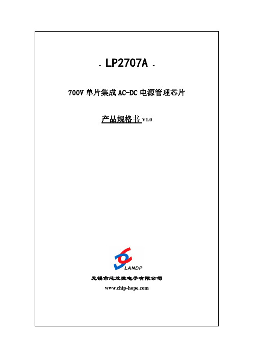
LP2707A
700V 单片集成 AC-DC 电源管理芯片
象。
4、自动重启动.
一旦出现故障,例如在输出过载、输出短路或开环情况下,
LP2707A进入自动重启动操作。每当FB引脚电压拉高时,一个由
振荡器记时的内部记数器会重新置位。如果40ms内FB引脚未被拉 高,功率MOSFET开关通常被禁止约1秒。自动重启动电路对功率
图 4 重启漏电波形
MOSFET进行交替使能和关闭,直到故障排除为止。上图4显示了输出短路时自动重启动电路
专为高性价比AC/DC转换器设计,主要用于适配器、开放式电源、LED照明,以及电器、 工业系统、电表等使用电源。
芯片采用开/关控制方式,提供一个灵活的设计方案,并且实现更低的系统成本及更大 的输出功率范围。该电源控制器可工作于典型的反激式电路拓扑中,构成简洁的AC/DC转换 器。LP2707A为SOP8封装。表1为输出功率表,图1为典型待机电源应用。
无锡ww市w.芯ch茂ip微-h电op子e.有c无o限wm锡w公w市.司c芯hi茂p-微ho电pe子.c有om限公司
- LP2707A -
700V 单片集成 AC-DC 电源管理芯片 产品规格书 V1.0
无锡市芯茂微电子有限公司
无锡ww市w.芯ch茂ip微-h电op子e.有c无o限wm锡w公w市.司c芯hi茂p-微ho电pe子.c有om限公司
LP2707A
700V 单片集成 AC-DC 电源管理芯片
3、过热保护.
热关断电路检测硅片的温度。阈值设置在140°C(典型)并具备45°C(典型)的迟滞范围。
当芯片温度超过这个阈值,功率MOSFET关闭,直到结温度下降到75°C,MOSFET才会重新开
启。采用75°C的迟滞可防止因持续故障而使PCB板出现过热现
L272中文资料
inch TYP. MAX.
OUTLINE AND MECHANICAL DATA
0.055 0.020 0.020 0.787 0.346 0.100 0.700 0.280 0.201 0.130
Powerdip 16
0.050
7/10
元器件交易网
L272
mm DIM. MIN. A a1 B b b1 D E e e3 e4 F I L Z 3.18 7.95 2.54 7.62 7.62 6.6 5.08 3.81 1.52 0.125 0.51 1.15 0.356 0.204 1.65 0.55 0.304 10.92 9.75 0.313 0.100 0.300 0.300 0.260 0.200 0.150 0.060 TYP. 3.32 0.020 0.045 0.014 0.008 0.065 0.022 0.012 0.430 0.384 MAX. MIN. TYP. 0.131 MAX. inch
Top Tstg, Tj
THERMAL DATA
Symbol Rth j-case Rth j-amb Rth j-alumina Parameter Thermal Resistance Junction-pins Thermal Resistance Junction-ambient Thermal Resistance Junction-alumina Max. Max. Max. Powerdip 15 70 – SO16 – – ** 50 Minidip * 70 100 – Unit
mm TYP. MAX. 1.75 0.25 1.6 0.46 0.25 0.5 45˚ (typ.) 10 6.2 1.27 8.89 4 5.3 1.27 0.62 8˚(max.) 0.150 0.181 0.016 0.386 0.228 0.014 0.007 0.004 MIN.
CW1274 Datasheet说明书
CW1274 4~7节电池保护IC功能特性●过充电保护•阈值范围3.650V、3.850V、4.175V~4.350V,25mV步进,±25mV精度●过放电保护•阈值范围2.300V~2.800V,100mV步进,±30mV精度●放电过流保护•过流检测1阈值范围0.050V~0.100V,±5mV精度•过流检测2阈值范围0.100V~0.200 V,,±10mV精度•短路保护阈值范围0.200V~0.500V,±20mV精度●充电过流保护•阈值范围-0.010V~-0.050V,±5mV精度●温度检测功能充放电高低温保护,温度外部可设●均衡功能●断线检测功能●负载检测功能●级联功能●低功耗设计•工作状态20μA (25°C)•休眠状态5μA (25°C)●封装形式:SSOP24应用领域●吸尘器●电动工具●电动自行车●后备电源●锂离子及锂聚合物电池包基本描述CW1274系列产品是一款高度集成的4~7串锂离子电池或锂聚合物电池保护芯片。
CW1274为电池包提供过充、过放、充放电过流、断线、充放电过温保护以及均衡功能,并支持芯片级联使用。
CW1274 典型应用框图CW1274产品选择指南CW1274 X X X X封装形式,S: SSOP24参数类型,从A到Z电池类型,L:代表锂离子电池F:代表磷酸铁锂电池功能和版本信息,从A 到Z产品目录CW1274 引脚排列图CW1274CW1274 绝对最大额定值注意:绝对最大额定值是指无论在任何条件下都不能超过的额定值。
如果超过此额定值,有可能造成产品损伤。
ESD等级额定工作电压CW1274电气特性除特殊说明外T A=25°CCW1274*2充放电温度保护温度取决于不同电阻的设定,放电低温保护温度默认为充电过温保护温度-20℃,即充电低温保护温度为0℃,则放电低温保护温度为-20℃*3所有过电流保护(包括过流1,过流2和短路保护)解除延迟时间均为60msCW1274原理框图CW1274 功能描述正常状态所有电池电压处于过充检测电压(V OC)和过放检测电压(V OD)之间,且CS端子电压处于过流检测电压(V EC1)和充电过流检测电压(V COC)之间时,CW1274处于正常工作状态。
28202;中文规格书,Datasheet资料
599 Menlo Drive, Suite 100Rocklin, California 95765, USAOffice: (916) 624-8333Fax: (916) 624-8003General: info@Technical: support@Web Site: Educational: Gripper Kit for the Boe-Bot® Robot (#28202)The Gripper KitThis kit allows your Parallax Boe-Bot® Robot to pick up objects. TheBoe-Bot robot (#28132 serial or #28832 USB) is sold separately.Before getting started, take an inventory of the parts in your kit. UseFig #1 to identify each part to the parts list. Once you haveinventoried your kit, proceed to Step #1.11423456791011121315161783Recommended Tools•Small needle nosed pliers•Phillips #2 point screwdriver•Small flat-blade screwdriver• A sharp-tipped hobby knife,such as an X-Acto® knife-OR-A hand drill with 5/64″ bitWARNING!DO NOT use electricscrewdrivers with this kit. Pleaseassemble using hand tools onlyto avoid damaging your Gripper.Step #1: SpacersItem Qty Description 4 (2) Gripper link 5 (2) #4 x 1" spacer• Insert spacers into plastic Gripper links. • Use Fig #2 as a guide to install the spacers. Whendone, the pieces will appear as shown in Fig #3.Fig #2Fig #3Step #2: Gripper LinksItem Qty Description6 (1) Gripper plate7 (2) 4-40 x 1.25" pan head screw8 (2) 4-40 Hex Nut•Be sure the angled portions on top of the plastic links match the angles on top of the Gripper as shown in Fig #5.• Move links and spacers into the Gripper plate, thensecure with 4-40 screws and nuts as shown in Fig #4. • Tighten securely.• Before continuing, double check your work to ensurethat the pieces are angled as in Fig #5.Fig #4 Fig #5Step #3: Foam TapeItem Qty Description14 (4) foam tape• Cut four pieces of foam tape, each 2 inches long. •Apply foam tape to the Gripper plate as shown in Fig #7.This completes the left-side Gripper sub-assembly.Fig #6Fig #7Step #4: Second Gripper Sub-assemblyItem Qty Description4 (2) Gripper link5 (2) #4 x 1" spacer6 (1) Gripper plate7 (2) 4-40 x 1.25" pan head screw8 (2) 4-40 hex nut 14 (4) foam tape• Repeat Steps #1 through #3 to build the right-sideGripper sub-assembly in a similar fashion.• Be sure the angled portions of the links match with theGrippers face to face. Position the pieces exactly as they appear in Fig #8.• Double check your work, then proceed to Step #5.Fig #8•Assemble the Gripper sub-assemblies to the upperand lower linkage plates as shown in Fig #9. In turn, insert each plastic link, a spacer, and secure with 4-40 screws and nuts.• When all four plastic links are installed, tighten securely.•Double check your work against Fig #10. Note that the hinge tabs on the bottom plate face up, while hinge tabs on top plate face down.Step #5: Linkage PlatesItem Qty Description3 (2) linkage plate 5 (4)#4 x 1" spacer 7(4) 4-40 x 1.25" pan head screw 8 (4) 4-40 hex nutStep #6: Control ArmsItem Qty Description 10 (2) control arm 15 (4) 4-40 x ¼" pan head screw• Attach control arms with 4-40 x ¼" screws as shown in Fig #11.•Final assembly must match Fig #12. Double check your work, then proceed to Step #7.Fig #11Fig #12Step #7: E-Z ConnectorsItem Qty Description 13 (2) Brass 0.072 E-Z Connector• Follow the directions on the package to install the E/Z Connector into the control arms. Use the nylon washers, but set the screws aside for now.• Check your work; your final assembly should match Fig #13.Fig #13Step #8: Install Gripper Hinge PlateItem Qty Description1 (1) hinge mount 15 (3) 4-40 x ¼" pan head screw 8 (3) 4-40 hex nutNote: It is recommended that the servos and tires on the Boe-Bot be installed with the wheels biased toward the front of the unit as shown below. This will prevent the Boe-Bot from tipping when it picks up objects.• Attach hinge mount to the Boe-Bot with the 4-40 x ¼" screws and nuts as shown in Fig #14 and Fig #15. • Double check your work against Fig #16.Fig #14 Top ViewFig #15 Bottom ViewFig #16Assembled ViewStep #9: Position Gripper on Boe-BotItem Qty Description(1) Gripper assembly (1) Boe-Bot robot• Remove one wheel to allow for dowel pin installation in the next step, Step #10.• Position the Gripper assembly onto the hinge mount as shown in Fig #17 below.•Place the top hinge tabs over the tabs on the hinge mount so the top of the Gripper stays on the hinge mount.Fig #17Step #10: Insert Dowel Pin Item Qty Description2 (1) dowelpin• Insert dowel pin.•If dowel pin slips in very easily, use needle nose pliers to slightly crimp the center of the hinge plate.• Replace wheel.Fig #18Fig #19Fig #21Step #12: Servo BracketsItem Qty Description16 (2) servo brackets 17 (4) 4-40 x 3/8" pan head screw 8 (4) 4-40 hex nut 11 (1) Parallax Standard Serv o• Attach servo brackets to servo with 4-40 screws and nuts. Make sure the metal brackets are placed below the plastic servo tabs as shown in Fig #22.•The final assembly should match Fig #23. Double check your work, then proceed to Step #13.Note: Only one arm of the servo horn is shown for clarity.Fig #22Fig #23Step #13: Bend Actuator RodItem Qty Description 12 (1) actuator rod•Using the needle nose pliers, bend actuator rod at mid-point. Then bend as shown in Fig #24.Fig #24Step #14: Install Actuator Rod Item Qty Description12 (1) actuatorrod11 (1) Parallax Standard Servo•Thread bent rod through servo horn as shown in Fig #25.Fig #25分销商库存信息: PARALLAX 28202。
L272AM,L272M,L272AD2TF,L272D2,L272AD2, 规格书,Datasheet 资料
©2009 Fairchild Semiconductor CorporationRev. 1.0.3Features•Output Current up to 0.7A•Operates at Low V oltage (V S(MIN) = 4V)•Low Saturation V oltage (Ip = 0.5A, V O = 1.5V)•Thermal Shutdown (TSD = 160°C)•Ground Compatible Inputs•Large Common Mode & Differential Mode RangeApplications•Servo Amplifier •Power Supply•Compact Disc •VCR •MonitorDescriptionThe L272 and L272A are high-power dual operational amplifier provided as a 8-DIP and 16-SOP package. The operational amplifier is designed for low impedance loads and will deliver output current up to 0.7A. The L272A offers tighter specifications for input bias current, input offset volt-age and input offset currents. The L272 and L272A can be used in a wide range of applications including power supply,VCR, monitor, servo amplifier, compact disc, etc.8-DIP1116-SOPL272/L272ADual Power Operational AmplifierDUAL POWER OPERATIONAL AMPLIFIER2Pin DefinitionsAbsolute Maximum Ratings (Note1)Note 1: The “Absolute Maximum Ratings” are those values beyond which the safety of the device cannot be guaranteed. The device should not be operated at these limits. The parametric values defined in the Electrical Characteristics tables are not guaranteed at the absolute maximum ratings.Thermal DataPin Number Pin Name Pin Function Description8-DIP 16-SOP116OUTPUT1Amp Output 121VCC Positive Supply Voltage 32OUTPUT2Amp Output 244/5/12/13VEE/GND Negative Supply Voltage (GND)57INPUT-2Amp Negative Input 268INPUT+2Amp Positive Input 279INPUT+1Amp Positive Input 1810INPUT-1Amp Negative Input 1Parameter Symbol Value Unit Supply Voltage V CC 40V Input VoltageV I V S V Differential Input Voltage V I(DIFF)±V S V DC Output CurrentI O 0.7A Peak Output Current (Non Repetitive)I P 1A Power Dissipation At: T amb = 50°C P tot 1W Operating Temperature Range T op -25 to 85°C Storage and Junction TemperatureT stg , T j-40 to 150°CParameterSymbol Value Unit Thermal Resistance Junction-Ambient Max.8-DIP 16-SOPR θja100190°C/WDUAL POWER OPERATIONAL AMPLIFIER3Electrical Characteristics (L272)( V CC = +12V, V EE = -12V, T A = 25°C unless otherwise specified )Note 2: Guaranteed by design. Not 100% tested in production.ParameterSymbol ConditionsMin.Typ.Max.Unit Supply Voltage (V CC - V EE )V S -4-28V Supply Current I S V O = V CC /2V CC = 24V, V EE = 0V V CC = 12V, V EE = 0V-87.51211mA mA Input Bias Current I BIAS --0.3 2.5μA Input Offset Voltage V IO --1560mV Input Offset Current I IO --50250nA Slew RateSR Vin = 1Vpp, Unit Gain-1-V/μs Gain-Bandwidth Product GBW --350-kHz Input ResistanceR I -500--k ΩLarge-Signal Voltage Gain G VV O(pp) = ±10V 6575-dB Input Noise Voltage e NB = 20kHz -10-μV Input Noise CurrentI N B = 20kHz-200-pA Common Mode Rejection Ratio CMRR -6075-dB Supply Voltage Rejection Ratio PSRR V CC = +15V, V EE = -15V V CC = +5V, V EE = -5V 5462-dB Output Voltage Swing V O V CC = 24V, V EE = 0V Ip = 0.1A Ip = 0.5A21212322.5--V V Channel Separation C S f = 1kHz, R L = 10Ω, G V = 30dB-60-dB Total Harmonic Distortion THD f = 1kHz, G V = 1dB, R L = ∞-0.5-%Thermal stutdown Temperature (Note2)TSD--160-°CDUAL POWER OPERATIONAL AMPLIFIER4Electrical Characteristics (L272A)( V CC = +12V, V EE = -12V, T A = 25°C unless otherwise specified )Note 3 : Guaranteed by design. Not 100% tested in production.ParameterSymbol ConditionsMin.Typ.Max.Unit Supply Voltage (V CC - V EE )V S -4-28V Supply Current I S V O = V CC /2V CC = 24V, V EE = 0V V CC = 12V, V EE = 0V-87.51211mA mA Input Bias Current I BIAS --0.11μA Input Offset Voltage V IO --730mV Input Offset Current I IO --20100nA Slew RateSR Vin = 1Vpp, Unit Gain-1-V/μs Gain-Bandwidth Product GBW --350-kHz Input ResistanceR I -500--k ΩLarge-Signal Voltage Gain G VV O(pp) = ±10V 6575-dB Input Noise Voltage e NB = 20kHz -10-μV Input Noise CurrentI N B = 20kHz-200-pA Common Mode Rejection Ratio CMRR -6075-dB Supply Voltage Rejection Ratio PSRR V CC = +15V, V EE = -15V V CC = +5V, V EE = -5V 5462-dB Output Voltage Swing V O V CC = 24V, V EE = 0V Ip = 0.1A Ip = 0.5A21212322.5--V V Channel Separation C S f = 1kHz, R L = 10Ω, G V = 30dB-60-dB Total Harmonic Distortion THD f = 1kHz, G V = 1dB, R L = ∞-0.5-%Thermal stutdown Temperature (Note3)TSD--160-°CDUAL POWER OPERATIONAL AMPLIFIER5Typical Performance CharacteristicsFigure 1. Supply Voltage vs SupplyCurrent with No LoadFigure 2. Open Loop Voltage GainFigure 3-1. Output Voltage Swing vs Load Current Figure 3-2. Output Voltage Swing vs Load CurrentFigure 4. Channel Separation vs FrequencyDUAL POWER OPERATIONAL AMPLIFIER6Applications< Tilt Coil Current Control Circuit in Monitor, 8-DIP Package>Tilt Coil33ΩV EE3.3uF 50V12387+-CH141k ΩCH2+-V EE40k Ω9.1k Ω10k Ω36k ΩV CC2465INDUAL POWER OPERATIONAL AMPLIFIER7Mechanical DimensionsPackageDimensions in millimeters8-DIPDUAL POWER OPERATIONAL AMPLIFIERMechanical Dimensions (Continued)PackageDimensions in millimeters16-SOP8DUAL POWER OPERATIONAL AMPLIFIER9Ordering InformationProduct NumberPackagePackingOperating TemperatureL272M 8-DIP Tube -25°C ~ +85°CL272D216-SOP Tube L272D2TF 16-SOP Tape and ReelL272AM 8-DIP Tube L272AD216-SOP Tube L272AD2TF16-SOPTape and ReelDUAL POWER OPERATIONAL AMPLIFIER11/18/09 0.0m 001Stock#DS400471© 2009 Fairchild Semiconductor CorporationLIFE SUPPORT POLICYFAIRCHILD’S PRODUCTS ARE NOT AUTHORIZED FOR USE AS CRITICAL COMPONENTS IN LIFE SUPPORT DEVICES OR SYSTEMS WITHOUT THE EXPRESS WRITTEN APPROVAL OF THE PRESIDENT OF FAIRCHILD SEMICONDUCTOR CORPORATION. As used herein:1.Life support devices or systems are devices or systemswhich, (a) are intended for surgical implant into the body, or (b) support or sustain life, and (c) whose failure to perform when properly used in accordance with instructions for use provided in the labeling, can bereasonably expected to result in a significant injury of the user.2. A critical component in any component of a life supportdevice or system whose failure to perform can bereasonably expected to cause the failure of the life support device or system, or to affect its safety or effectiveness.DISCLAIMERFAIRCHILD SEMICONDUCTOR RESERVES THE RIGHT TO MAKE CHANGES WITHOUT FURTHER NOTICE TO ANY PRODUCTS HEREIN TO IMPROVE RELIABILITY, FUNCTION OR DESIGN. FAIRCHILD DOES NOT ASSUME ANYLIABILITY ARISING OUT OF THE APPLICATION OR USE OF ANY PRODUCT OR CIRCUIT DESCRIBED HEREIN; NEITHER DOES IT CONVEY ANY LICENSE UNDER ITS PATENT RIGHTS, NOR THE RIGHTS OF OTHERS.。
- 1、下载文档前请自行甄别文档内容的完整性,平台不提供额外的编辑、内容补充、找答案等附加服务。
- 2、"仅部分预览"的文档,不可在线预览部分如存在完整性等问题,可反馈申请退款(可完整预览的文档不适用该条件!)。
- 3、如文档侵犯您的权益,请联系客服反馈,我们会尽快为您处理(人工客服工作时间:9:00-18:30)。
L2720/2/4July 2003LOW DROP DUAL POWER OPERATIONAL AMPLIFIERS®.OUTPUT CURRENT TO 1 A.OPERATES AT LOW VOLTAGES .SINGLE OR SPLIT SUPPLY.LARGE COMMON-MODE AND DIFFEREN-TIAL MODE RANGE.LOW INPUT OFFSET VOLTAGE .GROUND COMPATIBLE INPUTS .LOW SATURATION VOLTAGE .THERMAL SHUTDOWN .CLAMP DIODEDESCRIPTIONThe L2720, L2722 and L2724 are monolithic inte-grated circuits in powerdip, minidip and SIP-9 pack-ages, intended for use as power operational ampli-fiers in a wide range of applications including servo amplifiers and power supplies.They are particularly indicated for driving, inductive loads, as motor and finds applications in compact-disc VCR automotive, etc.The high gain and high output power capability pro-vide superior performance whatever an operational amplifier/power booster combination is required.POWERDIP(8 + 8)MINIDIP (Plastic)SIP9ORDERING NUMBERS : L2720 (Powerdip)L2722 (Minidip)L2724 (SIP9)1/10PIN CONNECTIONS (top views)L2720L2722L2724BLOCK DIAGRAML2720L2722L2724 SCHEMATIC DIAGRAM (one section)ABSOLUTE MAXIMUM RATINGSSymbol Parameter Value Unit V S Supply Voltage28V V S Peak Supply Voltage (50ms)50V V i Input Voltage V sV i Differential Input Voltage±V sI o DC Output Current1AI p Peak Output Current (non repetitive) 1.5AP tot Power Dissipation at T amb = 80o C (L2720), T amb = 50o C (L2722)T case = 75o C (L2720)T case = 50o C (L2724)1510WT stg, T j Storage and Junction Temperature–40 to 150o CTHERMAL DATASIP-9Powerdip MinidipR th j-case Thermal Resistance Junction-case Max.10o C/W15o C/W70o C/WR th j-amb Thermal Resistance Junction-ambient Max.70o C/W70o C/W100o C/W ELECTRICAL CHARACTERISTICSV s = 24V, T amb = 25o C unless otherwise specifiedSymbol Parameter Test Conditions Min.Typ.Max.Unit V s Single Supply Voltage428V V s Split Supply Voltage± 2± 14VI s Quiescent Drain Current V o=V s2V s = 24V1015mAV s = 8V915I b Input Bias Current0.21µA V os Input Offset Voltage10mV I os Input Offset Current100nA SR Slew Rate2V/µs B Gain-bandwidth Product 1.2MHz R i Input Resistance500kΩG v O.L. Voltage Gain f = 100Hzf = 1kHz 708060dBe N Input Noise VoltageB = 22Hz to 22kHz 10µVI N Input Noise Voltage200pA CMR Common Mode Rejection f = 1kHz6684dBSVR Supply Voltage Rejection f = 100Hz V s = 24VR G = 10kΩV s = ±12VV R = 0.5V V s = ±6V 60707580dBV DROP(HIGH)V s = ±2.5V to ±12V I p = 100mAI p = 500mA 0.71 1.5VV DROP(LOW)V s = ±2.5V to ±12V I p = 100mAI p = 500mA 0.30.51VC s Channel Separation f = 1KHz V s = 24VR L = 10ΩV s = 6VG v = 30dB 6060dBT sd Thermal Shutdown JunctionTemperature145o C Figure 1 :Quiescent Current vs. Supply Voltage FIgure 2 : Open Loop Gain vs. FrequencyFigure 3 : Common Mode Rejection vs.Frequency Figure 4 : Output Swing vs. Load Current(V S = ± 5 V.Figure 5 : Output Swing vs. Load Current(V S = ± 12 V.Figure 6 : Supply Voltage rejection vs.FrequencyFigure 7 :Channel Separation vs. FrequencyAPPLICATION SUGGESTIONIn order to avoid possible instability occuring into fi-nal stage the usual suggestions for the linear power stages are useful, as for instance :-layout accuracy ;-A 100nF capacitor connected between supply pins and ground ;-boucherot cell (0.1 to 0.2 µF + 1Ω series) be-tween outputs and ground or across the load.With single supply operation, a resistor (1k Ω)between the output and supply pin can be necessary for stability.Figure 8 : Bidirectional DC Motor Control with µP Compatible InputsV S1 = logic supply voltage Must be V S2 > V S1E1, E2 = logic inputsFigure 9 :Servocontrol for Compact-discFigure 10 :Capstan Motor Control in VideoRecordersFigure 11 : Motor Current Control CircuitNote :The input voltage level is compatible with L291 (8 - BIT D/A converter)Figure 12 :Bidirectional Speed Control of DC Motors2R3 . R1For circuit stability ensure that R X >where R M = internal resistance of motor.RMV S2R3 . R1 The voltage available at the terminals of the motor is V M = 2 (V I −) + |R O|. I M where |R O| =2 R X and I M is the motor current.Figure 13 :VHS-VCR Motor Control CircuitDIM.mm inchMIN.TYP.MAX.MIN.TYP.MAX. a10.510.020B0.85 1.400.0330.055 b0.500.020b10.380.500.0150.020 D20.00.787 E8.800.346e 2.540.100e317.780.700F7.100.280 I 5.100.201L 3.300.130Z 1.270.050Powerdip 16 OUTLINE ANDMECHANICAL DATAOUTLINE AND MECHANICALDATADIM.mminch MIN.TYP .MAX.MIN.TYP .MAX.A 3.320.131a10.510.020B 1.15 1.650.0450.065b 0.3560.550.0140.022b10.2040.3040.0080.012D 10.920.430E 7.959.750.3130.384e 2.540.100e37.620.300e47.620.300F 6.60.260I 5.080.200L 3.18 3.810.1250.150Z1.520.060MinidipSIP9DIM.mminch MIN.TYP.MAX.MIN.TYP.MAX.A 7.10.280a1 2.730.1060.118B 230.90B324.80.976b10.50.020b30.851.60.0330.063C 3.30.130c10.430.017c2 1.320.052D 21.20.835d114.50.571e 2.540.100e320.320.800L 3.10.122L130.118L217.60.693L30.250.010L417.417.850.6850,702M 3.20.126N 10.039P0.150.006DNML 119d 1L 3L 2La 1e3b3b1B e c 1Ac2CPL 4SIP9B3OUTLINE AND MECHANICAL DATAInformation furnished is believed to be accurate and reliable. However, STMicroelectronics assumes no responsibility for the conse-quences of use of such information nor for any infringement of patents or other rights of third parties which may result from its use. No license is granted by implication or otherwise under any patent or patent rights of STMicroelectronics. Specification mentioned in this publication are subject to change without notice. This publication supersedes and replaces all information previously supplied. STMi-croelectronics products are not authorized for use as critical components in life support devices or systems without express written approval of STMicroelectronics.The ST logo is a registered trademark of STMicroelectronics© 2003 STMicroelectronics – Printed in Italy – All Rights ReservedSTMicroelectronics GROUP OF COMPANIESAustralia - Brazil - Canada - China - Finland - France - Germany - Hong Kong - India - Israel - Italy - Japan - Malaysia - Malta - Morocco -Singapore - Spain - Sweden - Switzerland - United Kingdom - United States.。