Cadence PSpice添加SPICE模型
(完整版)HSPICE与CADENCE仿真规范与实例..

电路模拟实验专题实验文档一、简介本实验专题基于SPICE(Simulation Program With Integrated Circuit)仿真模拟,讲授电路模拟的方法和spice仿真工具的使用。
SPICE仿真器有很多版本,比如商用的PSPICE、HSPICE、SPECTRE、ELDO,免费版本的WinSPICE,Spice OPUS等等,其中HSPICE和SPECTRE功能更为强大,在集成电路设计中使用得更为广泛。
因此本实验专题以HSPICE和SPECTRE作为主要的仿真工具,进行电路模拟方法和技巧的训练。
参加本实验专题的人员应具备集成电路设计基础、器件模型等相关知识。
二、Spice基本知识(2)无论哪种spice仿真器,使用的spice语法或语句是一致的或相似的,差别只是在于形式上的不同而已,基本的原理和框架是一致的。
因此这里简单介绍一下spice的基本框架,详细的spice语法可参照相关的spice教材或相应仿真器的说明文档。
首先看一个简单的例子,采用spice模拟MOS管的输出特性,对一个NMOS管进行输入输出特性直流扫描。
V GS从1V变化到3V,步长为0.5V;V DS从0V变化到5V,步长为0.2V;输出以V GS为参量、I D与V DS之间关系波形图。
*Output Characteristics for NMOSM1 2 1 0 0 MNMOS w=5u l=1.0uVGS 1 0 1.0VDS 2 0 5.op.dc vds 0 5 .2 Vgs 1 3 0.5.plot dc -I(vds).probe*model.MODEL MNMOS NMOS VTO=0.7 KP=110U+LAMBDA=0.04 GAMMA=0.4 PHI=0.7.end描述的仿真电路如下图,图2-1 MOS管输入输入特性仿真电路图得到的仿真波形图如下图。
从这个简单的spice程序中可以知道spice电路描述的主要组成部分。
如何向LTspice正确导入Spice模型
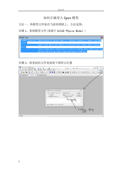
如何正确导入Spice模型
方法一、将模型文件粘在当前的图纸上,方法见图:步骤1:复制模型文件(来源于OrCAD PSpice Model )
步骤2:将复制的文件复制到下图所示位置
步骤3:点击上面框图中的OK,将文件粘贴在纸面上,然后从文件中拖一个三极管出来,将名字改成一样即可。
仿真效果见下图:
方法二、如有*.lib的库文件,比如PSPICE的日本晶体管库jbipolar.lib,将该文件考到LTC\LTspiceIV\lib\sub目录中。
然后按图操作:
点击OK后,效果如下所示:
仿真效果图如下:
Q2sc1907相频特性(30MHz截止频率)
方法三:将模型文件直接粘贴到LTC\LTspiceIV\lib\ cmp中的相应文件中。
如要将PSPICE的diode.lib的模型全导入到cmp中的standard.dio中。
先用记事本打开diode.lib,全选,复制。
而后用记事本打开standard.dio,在其适当的位置粘贴,关闭。
发现二极管库里多了很多元件(见下图)。
三极管同理。
原来二极管很少
多了很多二极管模型^_^。
spice使用简介

(1)电路图的绘制。绘制电路图,激 励为电压脉冲源,选用Source.olb库 中的VPULSE。
分别键入下面参数的名称和数值: V1=0V(初始值) TR=0.4μ s(上升时间) V2=5V(幅值) TF=0.5μ s(下降时间) TD=0(延迟时间) PER=20ms(周期) PW=10ms(脉冲宽度)
一个简单的RLC串联电路如图所示。试 用OrCAD对该电路电流频率响应进行交 流分析。
(1)电路图的绘制。
注意:信号源V1使用Source.olb库中的VAC模 型,幅值取1V。 在电路图中设置电流探针。单击 图标, 在欲测电流的元件(如R)支路上单击,放 置电流探针,如图所示。这样在执行PSpice 分析程序后不需要呼叫波形,探针测试的电 流便自动出现在波形输出窗口,支路电压、 节点电压和元件功率也可类似设置探针。
由图可知,流过电阻的电流会随着加在电阻 上的电压而随比例地增加。符合欧姆定律。
交流扫描分析(RLC电路的频率响应)
使用交流扫描分析(AC Sweep)来验
证R-L-C电路频谱图。 PSpice可对小信号线性电子电路进行交 流分析,此时半导体器件皆采用其线性 模型。它是针对电路性能因信号频率改 变而变动所作的分析,它能够获得电路 的幅频响应和相频响应以及转移导纳等 特性参数。
(2)创建新仿真文件,注意交流分析参数设 置方法,如下图所示。
(3)执行PSpice分析程序,其结果波形 见图所示。
标尺 上述的例题分析结果,如上图所示,如要想 从图形中得到精确的数值关系还需借助下面 要介绍的标尺(Cursors)的功能。其对应的 菜单如下图所示。
其快捷方式如下图所示,具体功能见表92。
一个电路设计能够使用PSpice分析 和优化的两个必备条件是:
Cadence cdsSPICE 使用说明

§ 1-2 建立可进行 SPICE 模拟的单元文件 主窗口分为信息窗口 CIW、命令行以及主菜单。信息窗口会给出一些系统信息(如出 错信息, 程序运行情况等) 。 在命令行中可以输入某些命令。 如我们调用 Cadence 的命令 icfb 和一些其它命令,比较重要的有调出帮助文件的 openbook&等。 一.File 菜单 在 File 菜单下,主要的菜单项有 New、Open、Exit 等。在具体解释之前我们不妨先理 顺一下以下几个关系。library(库)的地位相当于文件夹,它用来存放一整个设计的所有数据, 像一些子单元(cell)以及子单元(cell)中的多种视图(view) 。Cell(单元)可以是一个简 单的单元,像一个与非门,也可以是比较复杂的单元(由 symbol 搭建而成) 。View 则包含 多种类型,常用的有 schamatic,symbol,layout,extracted,ivpcell 等等,他们各自代表什 么意思以后将会一一提到。 New 菜单项的子菜单下有 Library、Cellview 两项。Library 项打开 New Library 窗口, Cellview 项打开 Create New File 窗口,如图 1-2-1 和 1-2-2 所示。
§ 1- 4
模拟的设置(重点)
Composer-schamatic 界面中的 Tools→Analog Artist 项可以打开 Analog Artist Simulation
图 1-4-1 Analog Artist Simulation 窗口 窗口,如图 1-4-1 所示。这是模拟时用到的主要工具,接下去主要介绍一下有关的内容。 一. Session 菜单 包括 Schematic Window、 Save State、 Load State、 Options、 Reset、 Quit 等菜单项。 Schematic window 项回到电路图;Save State 项打开相应的窗口,保存当前所设定的模拟所用到的各种
Cadence使用说明

第 5 页 共 97 页
第 1 页 共 97 页
Cadence cdsSPICE 使用说明
i——在光标处插入正文; x——删除光标处的字符; :wq——存盘退出; 要记著一点,在插入态处,不能打入指令,必需先按〈Esc〉键,返回指令态。假若户不知 身处何态,也可以按〈Esc〉键,不管处于何态,都会返回指令态其它的一些命令请读者自己参 阅有关的书籍。
vi 使用了两种状态,一是指令态(Command Mode),另一是插入态(Insert Mode)。当 vi 处于指令态时,打入的内容会视作指令来解释;而当 vi 处于插入态时,就可以打入正文 (text)文件;大多数 vi 指令是单字符的。由插入态改变为指令态,按〈Esc〉键;而由 命令态转为插入态,则可以使用下面的插入令,直接打入,无需再按〈Return〉键。在 vi 的指令态下,用 h,j,k,l 键移动光标,具体如下: h——光标左移一个字符; j——光标向下一行; k——光标向上一行; l——光标右移一个字符; 以下是一些基本插入命令(须用到的)的用法:
图 1-2-5 Library Path Editor 窗口 三.Technology File 菜单
这个菜单中的最后一项 Edit Layers 可以使用在版图编辑中,用来修改原始图层的一 些属性。
第 4 页 共 97 页
Cadence cdsSPICE 使用说明
§1-3 编辑可进行 SPICE 模拟的单元文件
名称晶体管模型(SPICE)到行为级模型(IBIS)的转换工具

名称:晶体管模型(SPICE)到行为级模型(IBIS)的转换工具
参考品牌:Cadence
参考型号:Cadence
数量:1套
技术参数:
1:含1个用户的PSpice 基本数模混合分析工具,辅助用户完成模拟及数字混合电路的仿真分析,包含有直流扫描、交流扫描、瞬态分析,温度参数扫描等功能,同时包含多样的仿真模型并具有建模功能。
2:含1个用户的PSpice 高级仿真分析工具,结合基本分析工具,使用户具备更加强大的分析功能,包括灵敏度分析,优化分析,蒙特卡洛分析,应力分析和参数测绘分析。
3:含1个用户的OrCAD SI信号完整性仿真工具,该工具支持布线前仿真和布线后后仿真两种工作流程,提供了针对PCB板极的信号仿真分析功能。
服务:
供方需要提供完整技术支持服务,包含仿真建模等的指导及培训内容。
验收合格后支付。
HOWTO Use a SPICE Model File in Cadence Allegro SPB 15.2

HOWTO Use a SPICE Model File in Cadence Allegro SPB 15.21.Obtain the SPICE model for the part you wish to simulate. For example, I obtained the followingSPICE model for a 2N3905 BJT from the Fairchild Semiconductor website:.model 2N3905 PNP(Is=1.41f Xti=3 Eg=1.11 Vaf=18.7 Bf=90.35 Ne=1.5 Ise=0+ Ikf=80m Xtb=1.5 Br=5.502 Nc=2 Isc=0 Ikr=0 Rc=2.5 Cjc=9.728p+ Mjc=.5776 Vjc=.75 Fc=.5 Cje=8.063p Mje=.3677 Vje=.75 Tr=35.05n+ Tf=179.3p Itf=.4 Vtf=4 Xtf=6 Rb=10)* Fairchild pid=66 case=TO92* 88-09-09 bam creationListing 1 Downloaded SPICE model for a 2N3905 bipolar junction transistor.2.Create an empty file named 2N3905.mod in some convenient location (e.g., your desktop).Note: The file extension must be “.mod”.ing any text editor program (e.g., NOTEPAD.EXE), open the file 2N3905.mod and copy thecontents of Listing 1 into the file. (Don’t close the text editor yet…)Note: In SPICE, name fields must begin with a letter. In Listing 1 the model name is “2N3905”. This model name is invalid because it does not start with a letter; it starts with the number 2.Note: In SPICE, BJT transistor names start with the letter ‘Q’.ing the text editor, change the model name from 2N3905 to Q2N3905. Save the file and exit thetext editor program..model Q2N3905 PNP(Is=1.41f Xti=3 Eg=1.11 Vaf=18.7 Bf=90.35 Ne=1.5 Ise=0+ Ikf=80m Xtb=1.5 Br=5.502 Nc=2 Isc=0 Ikr=0 Rc=2.5 Cjc=9.728p+ Mjc=.5776 Vjc=.75 Fc=.5 Cje=8.063p Mje=.3677 Vje=.75 Tr=35.05n+ Tf=179.3p Itf=.4 Vtf=4 Xtf=6 Rb=10)* Fairchild pid=66 case=TO92* 88-09-09 bam creationListing 2 Invalid model name 2N3905 changed to the valid name “Q2N3905”.5.If the Cadence Allegro Design Entry CIS program is not running, start it now. (Start » All Programs »Allegro SPB 15.2 » Design Entry CIS)6.Create a new Analog or Mixed A/D project. (File » New » Project… » New Project dialog » Analog orMixed A/D option » etc…)Note: On the New Project dialog (see Figure 1), there cannot be any spaces in the Name field or in the Location field.Note: On the New Project dialog, you must specify the project type as Analog or Mixed A/D if you want to perform PSpice simulations. The project type Schematic is strictly for schematiccapture; you cannot perform PSpice simulations with a Schematic project.Figure 1 New Project dialog7.On the Create PSpice Project dialog, select the options shown below and click on OK.Figure 2 Create PSpice Project dialog8.On the Allegro Design Entry CIS window, open the File menu and select the options New »PSpice Library. This starts the AMS Model Editor program (Figure 3).Figure 3 The AMS Model Editor window9.On the AMS Model Editor window, open the Model menu and select the Import… option.10.On the file Open dialog (Figure 4), browse to and select the file 2N3905.mod and then click Open.Figure 4 Import the file “2N3905.mod” into the AMS Model Editor program.11.On the AMS Model Editor window, open the File menu and select the Save As… option.12.On the Save As dialog (Figure 5), navigate to the folder that contains your project’s files (e.g.,MyProject). In the dialog’s File name field, specify a name for your model library file (e.g.,MySpiceModels) and then click on Save.Note: Remember that the Allegro software does not permit spaces in file names or folder names.Note: The file extension for a PSpice model library file must be “.lib”.Figure 5 Creating/saving a model library file in the folder that contains your project’s files.13.At this point the AMS Model Editor window should look something like Figure 6:Figure 6 AMS Model Editor window after saving the PSpice model library file.14.Exit the AMS Model Editor program (e.g., File » Exit).15.On the Allegro Design Entry CIS window, on the “project view” child window, expand the foldersPSpice Resources » Model Libraries and verify that the newly-created PSpice model library file .\myspicemodels.lib is listed under the Model Libraries folder.Figure 7 Project view window » PSpice Resources folder » Model Libraries folder » .\myspicemodels.lib.16.On the Allegro Design Entry CIS window, open the Tools menu and select the Generate Part…option.17.On the Generate Part dialog, click on the Browse… button that’s next to the Netlist/source file field.18.On the Browse File dialog, browse to and select the PSpice model library (.lib) file you created above(e.g., MySpiceModels.lib) and then click Open.Figure 8 Selecting the PSpice model library that you want to generate a schematic capture part from.19.Verify that the Generate Part dialog now looks similar to Figure 9, and then click OK. After a fewseconds delay the MicroSim Schematics To Capture Translator dialog (Figure 10) should appear briefly.Figure 9 The completed Generate Part dialog.Figure 10 MicroSim Schematics To Capture Translator dialog20.On the Allegro Design Entry CIS window, on the “project view” child window, expand the foldersDesign Resources » Library and verify that the newly-created schematic capture library file .\myspicemodels.olb is listed under the Library folder.Figure 11 Project view window » Design Resources folder » Library folder » .\myspicemodels.olb.21.On the Allegro Design Entry CIS window, expand the folders Design Resources » <proj_name>.dsn» SCHEMATIC1 and double-click on PAGE1 (see Figure 12).Figure 12 Project view window » Design Resources folder » mydemo.dsn » SCHEMATIC1 » PAGE1.22.On the Allegro Design Entry CIS window, locate the “Place Part” text entry field on the toolbar (seethe red arrow on Figure 13), type in the part number Q2N3905 as shown and then press the ENTER key on the keyboard.Figure 13ing the mouse, place one Q2N3905 part onto the schematic capture window. Press the escape(ESC) key on the keyboard to exit the part placement mode.Figure 1424.On the Allegro Design Entry CIS window, in the “Place Part” text entry field on the toolbar (see thered arrow on Figure 15), type in the part number 0 (press the numeric zero key on the keyboard) as shown and then press the ENTER key on the keyboard.ing the mouse, place one 0 (zero, a.k.a. “reference ground”) part slightly below the transistor’semitter leg (see Figure 16). Press the escape (ESC) key on the keyboard to exit the part placement mode.26.Press the W key to activate wiring mode, and wire the transistor’s collector, base, and emitterterminals to the ground reference part. When finished, press the escape (ESC) key to end the wiring mode.Note: This wiring scheme is admittedly weird. However, the goal at this point is to verify that the Q2N3905 part we created will actually simulate with PSpice. So we just need a simple, validcircuit at this point (which this circuit is), and not necessarily a “real world” circuit.Figure 16 A contrived but valid test circuit for the Q2N3905 part.27.On the Allegro Design Entry CIS window, click on the blue Run PSpice button on the toolbar (seeFigure 17).28.After a few seconds the Allegro AMS Simulator 210 window will appear and show you the results ofthe PSpice simulation (see Figure 18). If PSpice simulates the circuit successfully, the last line of output on the AMS Simulator window should be a warning message saying “All terminals aregrounded in this circuit” (see Figure 18).Figure 18 AMS Simulator 210 output showing the results of the PSpice simulation using the Q2N3905 part.29. A more comprehensive test might be a circuit and a simulation profile that produces a set of-I C versus V EC curves for the 2N3905 PNP transistor (see Figure 19 and Figure 20).Figure 19C EC Figure 20 Some -I C vs. V EC curves for the Q2N3905 PNP transistor VEC 0V 1.0V 2.0V 3.0V4.0V5.0V... -IC(Q1)0A 5mA10mAIB := [0..100uA] in 10uA steps。
基于PSPice的元器件建模方法研究

基于PSPice的元器件建模方法研究2.马鞍山学院实验工程中心,安徽马鞍山 234100摘要:随着智能制造2025的推进,本文提出一种基于Cadence软件下PSPice工具建立半导体器件模型方法的研究。
主要从三个方面建立器件的行为模型,包括:子电路建模、ABM建模、Model Editor工具(曲线拟合)建模的研究,通过对不同建模方法的比较,获得比较有效建模思路;最终通过借助Cadence软件的工具箱,对线性拟合和子电路的组合进行MOSFET的联合建模,采用Cadence软件的orcad模块,根据厂家提供的datasheet数据表建立MOSFET模型。
本文对建模方法的研究,有助于人们了解不同的的建模方法,可以为建模提供新的思路,有助于建立更加完善的模型。
关键字:器件建模;子电路建模ABM曲线拟合;联合建模[基金项目] 022年安徽省六卓越一拔尖项目“自动化专业卓越工程师”(2022zybj089);2022年马鞍山学院教学研究项目“智能制造背景下《电力电子技术》课程改革”(202201)。
[作者简介]王迪迪,男,汉族,安徽亳州人,硕士,助教,研究方向:半导体器件建模和电力电子与新能源发电。
引言随着半导体材料的不断发展,由其制成的新型电力电子器件也到飞速发展[1]。
一方面新器件的研制离不开器件的建模与仿真,另一方面新型研制的半导体器件,厂家一般只提供数据表,除非支付高昂的软件版权,否则并不提供免费的仿真软件,因此新型半导体器件的建模成为亟待解决的问题。
经过一段时间的文献调研、学习、资料整理及总结归纳,本文基于Cadence/PSPice软件工具以SiC MOSFET器件为例进行建模方法的研究。
传统的器件模型是根据材料的物理特性而建立的,而行为模型只关心器件的端口特性,从而建立的器件模型[2]。
通过对不同文献的阅读与资料的整理,摒弃了命令语句建模方法,以MOSFET 器件建模为例,重点研究了三种器件建模的方法即:通过capture平台搭建子电路建模,利用Model Editor工具建模,使用ABM库建模[1,3]。
- 1、下载文档前请自行甄别文档内容的完整性,平台不提供额外的编辑、内容补充、找答案等附加服务。
- 2、"仅部分预览"的文档,不可在线预览部分如存在完整性等问题,可反馈申请退款(可完整预览的文档不适用该条件!)。
- 3、如文档侵犯您的权益,请联系客服反馈,我们会尽快为您处理(人工客服工作时间:9:00-18:30)。
PSpice添加SPICE模型(图)
2012-03-03 20:32:59| 分类:通信技术| 标签:|字号大中小订阅
/s/blog_6c31e1650100q94t.html
在用PSpice进行仿真时,很多时候会遇到需要仿真的器件在PSpice自带的仿真库无法找到。
这时需要到该器件对应的官网上去下载对应的SPICE模型,而不同的公司提供的SPICE模型又都不尽相同,比如TI 公司提供MOD文件或TXT文本,而ADI公司提供的是CIR格式的文件。
如何将这些不同类型的SPICE 仿真模型转换成Simulation可用的lib文件呢?下面介绍了一个方法,只需简单几步即可实现将不同类型的SPICE Model(*.mod/*.txt/*.cir等文本文件)转换成*.lib、*.olb文件。
1、打开Model Editor(in PSpice Accessories)
2、File -> Open,打开*.mod或*.txt或*.cir文件
3、File -> Save as,另存为*.lib,即可得到Simulation用到的lib文件
4、File -> Export to Capture Part Library,得到*.olb文件,添加Capture库中,即可在原理图输入中使用该器件
5、最后一步,运行仿真时不要忘记将该lib文件添加到仿真库,Simulation Setting -> Configuration file -> library,add the *.lib file。