lm317 资料PDF
LM317中文资料PDF及电路图
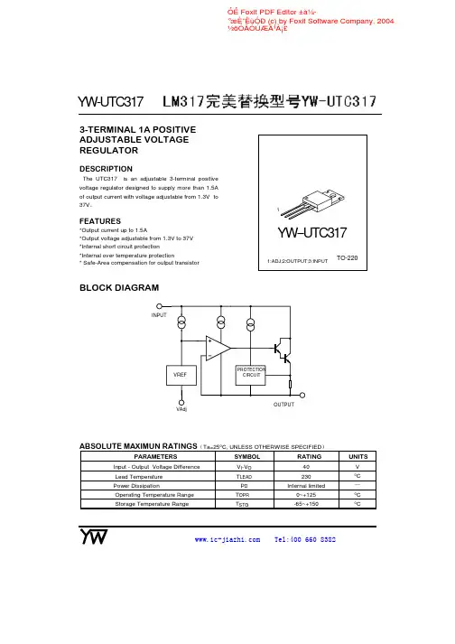
YW--UTC3173-TERMINAL 1A POSITIVE ADJUSTABLE VOLTAGE REGULATORDESCRIPTIONThe UTC317is an adjustable 3-terminal positivevoltage regulator designed to supply more than 1.5A of output current with voltage adjustable from 1.3V to 37VFEATURES*Output current up to 1.5A*Output voltage adjustable from 1.3V to37V *Internal short circuit protection*Internal over temperature protection*Safe-Area compensation for output transistorTO-22011:ADJ;2:OUTPUT;3:INPUTBLOCK DIAGRAMVAdjABSOLUTE MAXIMUN RATINGS Ta=25°C,UNLESS OTHERWISE SPECIFIEDPARAMETERSSYMBOLRATINGUNITSInput -Output Voltage Difference V I -V O 40VLead Temperature T LEAD 230°CPower DissipationP D Internal limitedüOperating Temperature Range T OPR 0~+125°C Storage Temperature RangeT STG-65~+150°CYW-UTC317ELECTRICAL CHARACTERISTICSV I -V O =5V,0°C <Tj<125°C,I O =500mA,I MAX =1.5A,P MAX =20W ,unless otherwise specifiedParameterSymbol Test conditionsMin TypMaxUnitLine Regulation∆V OTa=25°C,3V ≤V I -V O ≤40V 0.010.04%/VTa=0ü125°C,3V ≤V I -V O ≤40V0.020.07Ta=25°CV O ≤6V 1825mV Load Regulation ∆V O 10mA ≤I O ≤I MAX V O ≤5V 0.40.5%/V O 10mA ≤I O ≤I MAXV O ≤5V 4070mV V O ≤6V0.8 1.5%/V O Adjustable Pin current I ADJ 46100µA Adjustable Pin CurrentChange ∆IADJ 2.5V ≤V I -V O ≤40V,10mA ≤Io ≤I MAX ,P D ≤P MAX2.05µA Reference Voltage V REF 3V ≤V I -V O ≤40V,10mA ≤I O ≤I MAX ,P D ≤PMAX1.201.25 1.30V Temperature Stability STT 0.7%/V OMinimum Load Currentfor regulation I L(MIN)V I -V O =40V 3.510mA Maximum outputCurrentI O(MAX)V I -V O ≤15V,P D ≤P MAX 1.5 2.2AV I -V O ≤15V,P D ≤P MAX ,Ta=25°C0.150.4RMS Noise v.s.%of Vout eN T A =25°C,10H Z ≤f ≤10KH Z 0.0030.01%/V O Ripple Rejection RR V O =10V,f=120HZ,C ADJ =060dBV O =10V,f=120HZ,C ADJ =10µF6675Long-term Stability,T J =T HIGH ST T A =25°C,1000hr0.31%Junction to Case Thermal ResistanceR θJC5°C /WNote:Testing with low duty pulse should be used to avoid heating effect.YW-UTC317TYPICAL CHARACTERISTICS PERFORMANCETemperature O u t p u t V o l t a g e D e v i a t i o nFig.1.Load Regulation vstemperature-50-250255075100125354045505560Fig.2Adjustment Current vs TemperatureA d j u s t m e n t C u r r e n tTemperatureFig.3.Dropout Voltage vs Input-Temperature I n p u t -O u t p u t V o l t a g e D if f e r e n c eR e f e r e n c e V o l t a g eTemperatureTYPICAL APPLICATION CIRCUITSFig.5Programmable voltage regulatorFig.6Regulator with On-off controlVo=1.25V*(1+R2/R1)+Iadj*R2C1is required when regulator is located an appreciated distance from power supply.Co is needed to improve transient response.YW-UTC317Iomax=(VrefR1)+Iadj=1.25VR1Iomin=(VrefR1+R2)+Iadj=1.25VR1+R25mA<Io<100mA Fig.7Soft start application Fig.8Constant current applicationYW-UTC317。
LM317 三端稳压三极管
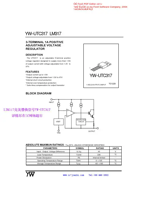
YW--UTC3173-TERMINAL 1A POSITIVE ADJUSTABLE VOLTAGE REGULATORDESCRIPTIONThe UTC317is an adjustable 3-terminal positivevoltage regulator designed to supply more than 1.5A of output current with voltage adjustable from 1.3V to 37VFEATURES*Output current up to 1.5A*Output voltage adjustable from 1.3V to37V *Internal short circuit protection*Internal over temperature protection*Safe-Area compensation for output transistorTO-22011:ADJ;2:OUTPUT;3:INPUTBLOCK DIAGRAMVAdjABSOLUTE MAXIMUN RATINGS Ta=25°C,UNLESS OTHERWISE SPECIFIEDPARAMETERSSYMBOLRATINGUNITSInput -Output Voltage Difference V I -V O 40VLead Temperature T LEAD 230°CPower DissipationP D Internal limitedüOperating Temperature Range T OPR 0~+125°C Storage Temperature RangeT STG-65~+150°CYW--UTC317 LM317ELECTRICAL CHARACTERISTICSV I-V O=5V,0°C<Tj<125°C,I O=500mA,I MAX=1.5A,P MAX=20W,unless otherwise specifiedParameter Symbol Test conditions Min Typ Max Unit Line Regulation∆V O Ta=25°C,3V≤V I-V O≤40V0.010.04%/VTa=0ü125°C,3V≤V I-V O≤40V0.020.07Ta=25°C V O≤6V1825mV Load Regulation∆V O10mA≤I O≤I MAX V O≤5V0.40.5%/V O10mA≤I O≤I MAX V O≤5V4070mVV O≤6V0.8 1.5%/V O Adjustable Pin current I ADJ46100µAAdjustable Pin CurrentChange ∆IADJ 2.5V≤V I-V O≤40V,10mA≤Io≤I MAX,P D≤P MAX2.05µAReference Voltage V REF3V≤V I-V O≤40V,10mA≤I O≤I MAX,P D≤PMAX1.20 1.25 1.30VTemperature Stability STT0.7%/V O Minimum Load Currentfor regulationI L(MIN)V I-V O=40V 3.510mAMaximum outputCurrentI O(MAX)V I-V O≤15V,P D≤P MAX 1.5 2.2AV I-V O≤15V,P D≤P MAX,Ta=25°C0.150.4 RMS Noise v.s.%of VouteN T A=25°C,10H Z≤f≤10KH Z0.0030.01%/V O Ripple Rejection RR V O=10V,f=120HZ,C ADJ=060dBV O=10V,f=120HZ,C ADJ=10µF6675Long-term Stability,T J=T HIGHST T A=25°C,1000hr0.31%Junction to CaseThermal ResistanceRθJC5°C/W Note:Testing with low duty pulse should be used to avoid heating effect.317TYPICAL CHARACTERISTICS PERFORMANCETemperature O u t p u t V o l t a g e D e v i a t i o nFig.1.Load Regulation vstemperature-50-250255075100125354045505560Fig.2Adjustment Current vs TemperatureA d j u s t m e n t C u r r e n tTemperatureFig.3.Dropout Voltage vs Input-Temperature I n p u t -O u t p u t V o l t a g e D if f e r e n c eR e f e r e n c e V o l t a g eTemperatureTYPICAL APPLICATION CIRCUITSFig.5Programmable voltage regulatorFig.6Regulator with On-off controlVo=1.25V*(1+R2/R1)+Iadj*R2C1is required when regulator is located an appreciated distance from power supply.Co is needed to improve transient response.317Iomax=(VrefR1)+Iadj=1.25VR1Iomin=(VrefR1+R2)+Iadj=1.25VR1+R25mA<Io<100mA Fig.7Soft start application Fig.8Constant current application317。
LM317T-PDF资料
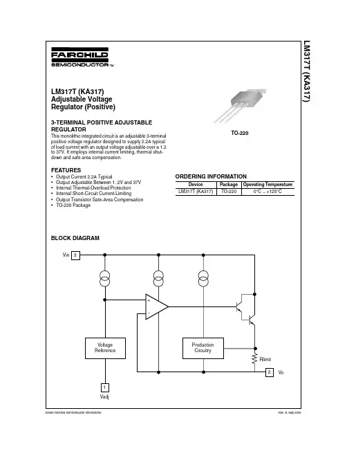
元器件交易网LM317T (KA317)LM317T (KA317) ABSOLUTE MAXIMUM RATINGS (T A = +25°C, unless otherwise speci fied)ELECTRICAL CHARACTERISTICS(V I - V O = 5V, I O = 0.5A, 0°C ≤ T J ≤ +125°C, I MAX = 1.5A, P MAX = 20W, unless otherwise specified)*Load and line regulation are specified at constant junction temperature. Change in V D due to heating effects must be taken into account separately. Pulse testing with low duty is used. (PMAX = 20W)CharacteristicSymbol Value Unit Input-Output Voltage DifferentialV I - V O 40V Lead T emperatureT LEAD 230°C Power DissipationP D Internally limited W Operating T emperature RangeT OPR 0 ~ +125°C Storage T emperature RangeT STG -65 ~ +125°C T emperature Coef ficient of Output Voltage V O /T 0.02%/°C CharacteristicSymbol Test Conditions Min Typ Max Unit Line RegulationRline T A = +25°C 3V ≤ V I - V O ≤ 40V 0.010.04%/V 3V ≤ V I - V O ≤ 40V 0.020.07%/V Load Regulation Rload T A = +25°C, 10mA ≤ I O ≤ I MAX V O < 5VV O ≥ 5V180.4250.5mV %/V O 10mA ≤ I O ≤ I MAX V O < 5VV O ≥ 5V400.8701.5mV %/V O Adjustable Pin Current I ADJ 46100µA Adjustable Pin Current Change ∆ I ADJ 3V ≤ V I - V O ≤ 40V10mA ≤ I O ≤ I MAX P ≤ P MAX2.05µA Reference Voltage V REF 3V ≤ V IN - V OUT ≤ 40V10mA ≤ I O ≤ I MAX P D ≤ P MAX1.20 1.25 1.30V T emperature Stability ST t 0.7%/V O Minimum Load Current to Maintain Regulation L (MIN) V I - V O = 40V3.512mA Maximum Output Current I O(MAX) V I - V O ≤ 15V , P D ≤ P MAX V I - V O ≤ 40V, P D ≤ P MAX , T A = 25°C1.02.20.3A RMS Noise, % of V OUT e N T A = +25°C, 10Hz ≤ f ≤ 10KHz0.0030.01%/V O Ripple Rejection RR V O = 10V , f = 120Hzwithout C ADJ C ADJ = 10µF666075dB Long-Term Stability, T J = T HIGH ST T A = +25°C for end pointmeasurements, 1000HR 0.31%Thermal Resistance Junction toCaseR θ JC 5°C/W 元器件交易网元器件交易网LM317T (KA317)TRADEMARKSThe following are registered and unregistered trademarks Fairchild Semiconductor owns or is authorized to use and is not intended to be an exhaustive list of all such trademarks.ACEx™Bottomless™CoolFET™CROSSVOLT™E2CMOS™FACT™FACT Quiet Series™FAST®FASTr™GTO™HiSeC™ISOPLANAR™MICROWIRE™POP™PowerTrench®QFET™QS™Quiet Series™SuperSOT™-3SuperSOT™-6SuperSOT™-8SyncFET™TinyLogic™UHC™VCX™DISCLAIMERFAIRCHILD SEMICONDUCTOR RESERVES THE RIGHT TO MAKE CHANGES WITHOUT FURTHER NOTICE TO ANY PRODUCTS HEREIN TO IMPROVE RELIABILITY, FUNCTION OR DESIGN. FAIRCHILD DOES NOT ASSUME ANY LIABILITY ARISING OUT OF THE APPLICATION OR USE OF ANY PRODUCT OR CIRCUIT DESCRIBED HEREIN; NEITHER DOES IT CONVEY ANY LICENSE UNDER ITS PATENT RIGHTS, NOR THE RIGHTS OF OTHERS.LIFE SUPPORT POLICYFAIRCHILD’S PRODUCTS ARE NOT AUTHORIZED FOR USE AS CRITICAL COMPONENTS IN LIFE SUPPORT DEVICES OR SYSTEMS WITHOUT THE EXPRESS WRITTEN APPROVAL OF FAIRCHILD SEMICONDUCTOR CORPORATION.As used herein:1. Life support devices or systems are devices or systems which, (a) are intended for surgical implant into the body, or (b) support or sustain life, or (c) whose failure to perform when properly used in accordance with instructions for use provided in the labeling, can be reasonably expected to result in significant injury to the user.2. A critical component is any component of a life support device or system whose failure to perform can be reasonably expected to cause the failure of the life support device or system, or to affect its safety or effectiveness.PRODUCT STATUS DEFINITIONSDefinition of TermsDatasheet Identification Product Status DefinitionAdvance Information Formative or InDesign This datasheet contains the design specifications for product development. Specifications may change in any manner without notice.Preliminary First Production This datasheet contains preliminary data, andsupplementary data will be published at a later date.Fairchild Semiconductor reserves the right to makechanges at any time without notice in order to improvedesign.No Identification Needed Full Production This datasheet contains final specifications. FairchildSemiconductor reserves the right to make changes atany time without notice in order to improve design.Obsolete Not In Production This datasheet contains specifications on a productthat has been discontinued by Fairchild semiconductor.The datasheet is printed for reference information only.元器件交易网。
lm317参数及中文使用手册
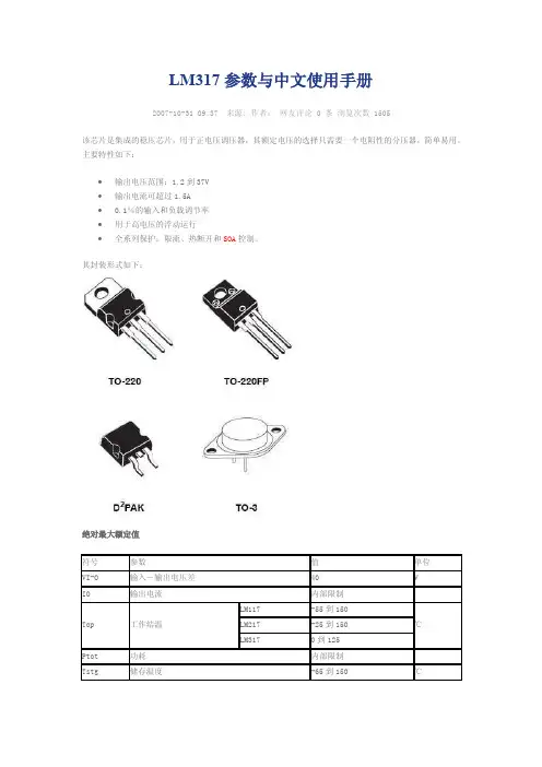
LM317参数与中文使用手册2007-10-31 09:37 来源: 作者:网友评论 0 条浏览次数 1505该芯片是集成的稳压芯片,用于正电压调压器,其额定电压的选择只需要一个电阻性的分压器,简单易用。
主要特性如下:∙输出电压范围:1.2到37V∙输出电流可超过1.5A∙0.1%的输入和负载调节率∙用于高电压的浮动运行∙全系列保护:限流、热断开和SOA控制。
其封装形式如下:绝对最大额定值引脚图(顶视)注:输入至少要比输出高2V,否则不能调压。
输入电要最高不能超过40V吧。
输出电流最好不超过1A。
输入12V的话,输出最高就是10V左右。
由于它内部还是线性稳压,因此功耗比较大。
当输入输入电压差比较大且输出电流也比较大时,注意317的功耗不要过大。
一般加散热片后功耗也不超过20W。
因此压差大时建议分档调压。
应用电路下面是赠送的两篇散文欣赏,可以仔细阅读,不需要的朋友可以下载后编辑删除!!谢谢!!脚下的时光不知走过多少地方,不知看过多少风景,不知听说过多少轶事;题记:蒲公英我走过很多地方,但是同样的,我也有更多的地方没去过!我渴望走遍地球上每一寸土地,我期许世界上每一个地方的人都善良!然而,现实的世界告诉我;理想的丰满一定要遇到拥有相同理想的另一半!我喜欢珠海,一个美丽的花园城市;我喜欢那里的天气,没有北方的寒冷;四季如春的温度感觉非常惬意,不用担心换季带来的差异!走在市区的街道上,绿化的花草树木被园丁修剪的井然有序;形态各异的花卉搭配得格外美观!尤其是除过草之后的绿地,泥土的芬芳与绿草的清新扑鼻而来,有一种身处大草原的感觉,使人心旷神怡!我时常一个人发呆,散步;看着过往的人群,车水马龙的街道;也时常去繁华的街巷,拥挤的商业中心;感觉这才是生活,正因为世界有了这么多事物的陪伴,才使我有了对美好生活的向往与喜悦!珠海的夜,很美;到处灯红酒绿,一派歌舞升平的祥和;每当夜幕降临,才是广东因有的生活的开始!溜冰场,酒吧,迪厅,大排档等等等等;我很庆幸在这里认识了很多人,他们教会了我很多,也帮助了我很多;我们都是来自五湖四海,为了同一个目标而聚集在一起的年轻人;我们时常出去聚会,嗨皮;但等到散场后,又回到了应有的孤寂!白天,可以去渔女,公园,九州城,免税店等等都是不错的地方!人常说,一个时代会有一个时代的代表;而我在这个曾经为之奋斗的地方,也时常会想起曾经相识的人,走过的地方,看过的风景;有时候,听着当时的流行歌曲,也会感伤;也会自嘲一笑;还有那公车到站的粤语提醒,还有那想见却永远没见的人;一篇篇,一幕幕久久回荡在脑海;早晨的肠粉,中午的餐饭,下午的炒粉,晚上的烧烤;好像味道还回味在口中一样!人,只有在对自己真诚的人的眼里,才会感觉到亲切;而我,也着实喜欢这座城市带给我家一样的温暖感觉!在这短暂而悠长的时光里,我成长了很多,也磨砺了很多;正是因为思想的成熟,阅历的增长,我选择了离开;去寻找属于自己的新的天地,新的开始,新的征程!其实,无论走过多少地方;都不重要!重要的是你从中得到什么!知识!阅历!思想!······每个人,在人生的道路上;难免遇到挫折困苦,也难免会因为一些因素而错失机缘!也不可能因为一时的过失而自暴自弃颓废一生!人,应该用豁达的心态来迎接下一秒的新鲜时光;而不是沉溺在上一秒的懊恼当中!每个人的路,都在自己的脚下;只有自己醒悟才能把未来的路走好,反之只会让错误延续到未来,从而影响以后的健康生活!即便曾经的时光再美好,那也只是人生道路上的一段插曲;没必要去纠结当时的愕然,愚昧!就像我,从来不对上一秒的事情产生情绪一样!一切都是恬淡的样子,顺其自然比什么都好!对于未来,只要真诚的去善待身边的所有;我相信,未来的时光,也该是你想象的模样!蒲公英2015.12.13家乡的茶籽林家乡高才坂,一年四季茶籽林郁郁葱葱,枝繁叶茂。
LM317中文资料大全
LM317中文资料大全LM117/LM317简介LM117/LM317是美国国家半导体公司的三端可调正稳压器集成电路。
我国和世界各大集成电路生产商均有同类产品可供选用,是使用极为广泛的一类串联集成稳压器。
LM117/LM317 的输出电压范围是1.2V 至37V,负载电流最大为1.5A。
它的使用非常简单,仅需两个外接电阻来设置输出电压。
此外它的线性调整率和负载调整率也比标准的固定稳压器好。
LM117/LM317 内置有过载保护、安全区保护等多种保护电路。
通常LM117/LM317 不需要外接电容,除非输入滤波电容到LM117/LM317 输入端的连线超过6 英寸(约15 厘米)。
使用输出电容能改变瞬态响应。
调整端使用滤波电容能得到比标准三端稳压器高的多的纹波抑制比。
LM117/LM317 能够有许多特殊的用法。
比如把调整端悬浮到一个较高的电压上,可以用来调节高达数百伏的电压,只要输入输出压差不超过LM117/LM317 的极限就行。
当然还要避免输出端短路。
还可以把调整端接到一个可编程电压上,实现可编程的电源输出。
LM117负电压输出LM317正电压输出LM317特性简介可调整输出电压低到1.2V保证1.5A 输出电流典型线性调整率0.01%页脚内容1典型负载调整率0.1%80dB纹波抑制比输出短路保护过流、过热保护调整管安全工作区保护标准三端晶体管封装电压范围LM117/LM317 1.25V 至37V 连续可调图1 LM317典型应用电路页脚内容2图2 LM317外形引脚图片D2PAK封典型的TO-3封装TO-220封装ISOWATT220封装装LM117LM117KLM217 LM217K LM217T LM217D2T页脚内容3LM317电气参数:页脚内容4页脚内容5页脚内容6SVR电源电压抑制Tj=25℃f=120HzCADJ =0 6665 -80 -dBCADJ=10uF80 -6680 -dBLM317如何应用计算图3决定LM317输出电压的是电阻R1,R2的比值,假设R2是一个固定电阻.因为输出端的电位高,电流经R1, R 2流入接地点. LM317的控制端消耗非常少的电流,可忽略不计.所以, 控制端的电位是I x R2,又因为LM317控制端, 输出端接脚间的电位差为1.25 V,所以Out(输出)的电压是:接下来,计算I: out与adj接脚间的电位差为1.25 V,电阻R1.电流I是: 1.25/R1。
LM317EMP
SOT-223 vs. D-Pak (TO-252) Packages
00906354
Scale 1:1
© 2004 National Semiconductor Corporation
DS009063
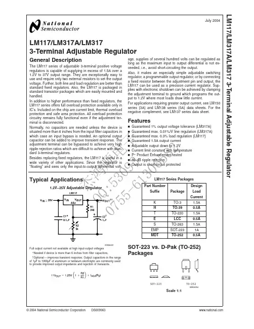
LM117/LM317A/LM317
Connection Diagrams
1.2V–25V Adjustable Regulator
Package TO-3
TO-39 LCC
TO-220 TO-263
SOT-223 TO-252
Full output current not available at high input-output voltages
*Needed if device is more than 6 inches from filter capacitors.
杰
Typical Applications
QQ 鸿 07 :5 顺电 55 30 -6 93 子 13 06 58 2
Part Number Suffix K T H E S EMP MDT
00906301
LM117 Series Packages Design Load Current 1.5A 0.5A 1.5A 0.5A 1.5A 1A 0.5A
Features
n n n n n n n n n Guaranteed 1% output voltage tolerance (LM317A) Guaranteed max. 0.01%/V line regulation (LM317A) Guaranteed max. 0.3% load regulation (LM117) Guaranteed 1.5A output current Adjustable output down to 1.2V Current limit constant with temperature P+ Product Enhancement tested 80 dB ripple rejection Output is short-circuit protected
lm317
LM117/LM317A/LM3173-Terminal Adjustable RegulatorGeneral DescriptionThe LM117series of adjustable 3-terminal positive voltage regulators is capable of supplying in excess of 1.5A over a 1.2V to 37V output range.They are exceptionally easy to use and require only two external resistors to set the output voltage.Further,both line and load regulation are better than standard fixed regulators.Also,the LM117is packaged in standard transistor packages which are easily mounted and handled.In addition to higher performance than fixed regulators,the LM117series offers full overload protection available only in IC’s.Included on the chip are current limit,thermal overload protection and safe area protection.All overload protection circuitry remains fully functional even if the adjustment termi-nal is disconnected.Normally,no capacitors are needed unless the device is situ-ated more than 6inches from the input filter capacitors in which case an input bypass is needed.An optional output capacitor can be added to improve transient response.The adjustment terminal can be bypassed to achieve very high ripple rejection ratios which are difficult to achieve with stan-dard 3-terminal regulators.Besides replacing fixed regulators,the LM117is useful in a wide variety of other applications.Since the regulator is “floating”and sees only the input-to-output differential volt-age,supplies of several hundred volts can be regulated as long as the maximum input to output differential is not ex-ceeded,i.e.,avoid short-circuiting the output.Also,it makes an especially simple adjustable switching regulator,a programmable output regulator,or by connecting a fixed resistor between the adjustment pin and output,the LM117can be used as a precision current regulator.Sup-plies with electronic shutdown can be achieved by clamping the adjustment terminal to ground which programs the out-put to 1.2V where most loads draw little current.For applications requiring greater output current,see LM150series (3A)and LM138series (5A)data sheets.For the negative complement,see LM137series data sheet.Featuresn Guaranteed 1%output voltage tolerance (LM317A)n Guaranteed max.0.01%/V line regulation (LM317A)n Guaranteed max.0.3%load regulation (LM117)n Guaranteed 1.5A output current n Adjustable output down to 1.2Vn Current limit constant with temperature n P +Product Enhancement tested n 80dB ripple rejectionnOutput is short-circuit protectedTypical ApplicationsLM117Series Packages and Power CapabilityPart NumberRatedDesign Suffix Package Power Load DissipationCurrent K TO-320W 1.5A H TO-392W 0.5A T TO-22020W 1.5A E LCC 2W 0.5A STO-2634W1.5ADS009063-1Full output current not available at high input-output voltages *Needed if device is more than 6inches from filter capacitors.†Optional—improves transient response.Output capacitors in the range of 1µF to 1000µF of aluminum or tantalum electrolytic are commonly used to provide improved output impedance and rejection of transients.May 1997LM117/LM317A/LM3173-Terminal Adjustable Regulator©1997National Semiconductor Corporation Absolute Maximum Ratings(Note1)If Military/Aerospace specified devices are required, please contact the National Semiconductor Sales Office/ Distributors for availability and specifications.Power Dissipation Internally Limited Input-Output Voltage Differential+40V,−0.3V Storage Temperature−65˚C to+150˚C Lead TemperatureMetal Package(Soldering,10seconds)300˚C Plastic Package(Soldering,4seconds)260˚C ESD Tolerance(Note5)3kV Operating Temperature RangeLM117−55˚C≤T J≤+150˚C LM317A−40˚C≤T J≤+125˚C LM3170˚C≤T J≤+125˚C PreconditioningThermal Limit Burn-In All Devices100%Electrical Characteristics(Note3)Specifications with standard type face are for T J=25˚C,and those with boldface type apply over full Operating Tempera-ture Range.Unless otherwise specified,V IN−V OUT=5V,and I OUT=10mA.Parameter Conditions LM117(Note2)UnitsMin Typ Max Reference Voltage V3V≤(V IN−V OUT)≤40V, 1.20 1.25 1.30V10mA≤I OUT≤I MAX,P≤P MAXLine Regulation3V≤(V IN−V OUT)≤40V(Note4)0.010.02%/V0.020.05%/V Load Regulation10mA≤I OUT≤I MAX(Note4)0.10.3%0.31%Thermal Regulation20ms Pulse0.030.07%/W Adjustment Pin Current50100µA Adjustment Pin Current Change10mA≤I OUT≤I MAX0.25µA3V≤(V IN−V OUT)≤40VTemperature Stability T MIN≤T J≤T MAX1% Minimum Load Current(V IN−V OUT)=40V 3.55mA Current Limit(V IN−V OUT)≤15VK Package 1.5 2.2 3.4AH,K Packages0.50.8 1.8A(V IN−V OUT)=40VK Package0.30.4AH,K Packages0.150.2A RMS Output Noise,%of V OUT10Hz≤f≤10kHz0.003% Ripple Rejection Ratio V OUT=10V,f=120Hz,65dBC ADJ=0µFV OUT=10V,f=120Hz,6680dBC ADJ=10µFLong-Term Stability T J=125˚C,1000hrs0.31% Thermal Resistance,K Package 2.33˚C/W Junction-to-Case H Package1215˚C/WE Package˚C/WThermal Resistance,Junction-K Package35˚C/W to-Ambient(No Heat Sink)H Package140˚C/WE Package˚C/W 2Electrical Characteristics(Note3)Specifications with standard type face are for T J=25˚C,and those with boldface type apply over full Operating Tempera-ture Range.Unless otherwise specified,V IN−V OUT=5V,and I OUT=10mA.Parameter Conditions LM317A LM317UnitsMin Typ Max Min Typ Max Reference Voltage 1.238 1.250 1.262V3V≤(V IN−V OUT)≤40V, 1.225 1.250 1.270 1.20 1.25 1.30V10mA≤I OUT≤I MAX,P≤P MAXLine Regulation3V≤(V IN−V OUT)≤40V(Note4)0.0050.010.010.04%/V0.010.020.020.07%/V Load Regulation10mA≤I OUT≤I MAX(Note4)0.10.50.10.5%0.310.3 1.5% Thermal Regulation20ms Pulse0.040.070.040.07%/W Adjustment Pin Current5010050100µAAdjustment Pin Current Change 10mA≤I OUT≤I MAX0.250.25µA 3V≤(V IN−V OUT)≤40VTemperature Stability T MIN≤T J≤T MAX11% Minimum Load Current(V IN−V OUT)=40V 3.510 3.510mA Current Limit(V IN−V OUT)≤15VK,T,S Packages 1.5 2.2 3.4 1.5 2.2 3.4AH Package0.50.8 1.80.50.8 1.8A(V IN−V OUT)=40VK,T,S Packages0.150.40.150.4AH Package0.0750.20.0750.2A RMS Output Noise,%of V OUT10Hz≤f≤10kHz0.0030.003% Ripple Rejection Ratio V OUT=10V,f=120Hz,6565dBC ADJ=0µFV OUT=10V,f=120Hz,66806680dBC ADJ=10µFLong-Term Stability T J=125˚C,1000hrs0.310.31% Thermal Resistance,Junction-K Package 2.33˚C/W to-Case H Package12151215˚C/WT Package454˚C/W Thermal Resistance,Junction-K Package3535˚C/W to-Ambient(No Heat Sink)H Package140140˚C/WT Package5050˚C/WS Package(Note6)5050˚C/W Note1:Absolute Maximum Ratings indicate limits beyond which damage to the device may occur.Operating Ratings indicate conditions for which the device is in-tended to be functional,but do not guarantee specific performance limits.For guaranteed specifications and test conditions,see the Electrical Characteristics.The guaranteed specifications apply only for the test conditions listed.Note2:Refer to RETS117H drawing for the LM117H,or the RETS117K for the LM117K military specifications.Note3:Although power dissipation is internally limited,these specifications are applicable for maximum power dissipations of2W for the TO-39and20W for theTO-3,TO-220,and TO-263.I MAX is1.5A for the TO-3,TO-220,and TO-263packages and0.5A for the TO-39package.All limits(i.e.,the numbers in the Min.and Max.columns)are guaranteed to National’s AOQL(Average Outgoing Quality Level).Note4:Regulation is measured at a constant junction temperature,using pulse testing with a low duty cycle.Changes in output voltage due to heating effects are covered under the specifications for thermal regulation.Note5:Human body model,100pF discharged through a1.5kΩresistor.Note6:If the TO-263package is used,the thermal resistance can be reduced by increasing the PC board copper area thermally connected to the package:Using0.5square inches of copper area.θJA is50˚C/W;with1square inch of copper area,θJA is37˚C/W;and with1.6or more square inches of copper area,θJA is32˚C/W.Typical Performance CharacteristicsOutput Capacitor =0µF unless otherwise notedLoad RegulationDS009063-37Current LimitDS009063-38Adjustment CurrentDS009063-39Dropout Voltage DS009063-40Temperature Stability DS009063-41Minimum Operating CurrentDS009063-42Ripple Rejection DS009063-43Ripple Rejection DS009063-44Ripple RejectionDS009063-45 4Typical Performance Characteristics(Continued)Application HintsIn operation,the LM117develops a nominal 1.25V reference voltage,V REF ,between the output and adjustment terminal.The reference voltage is impressed across program resistor R1and,since the voltage is constant,a constant current I 1then flows through the output set resistor R2,giving an out-put voltage ofSince the 100µA current from the adjustment terminal repre-sents an error term,the LM117was designed to minimize I ADJ and make it very constant with line and load changes.To do this,all quiescent operating current is returned to the output establishing a minimum load current requirement.If there is insufficient load on the output,the output will rise.External CapacitorsAn input bypass capacitor is recommended.A 0.1µF disc or 1µF solid tantalum on the input is suitable input bypassing for almost all applications.The device is more sensitive to the absence of input bypassing when adjustment or output capacitors are used but the above values will eliminate the possibility of problems.The adjustment terminal can be bypassed to ground on the LM117to improve ripple rejection.This bypass capacitor prevents ripple from being amplified as the output voltage is increased.With a 10µF bypass capacitor 80dB ripple rejec-tion is obtainable at any output level.Increases over 10µFdo not appreciably improve the ripple rejection at frequen-cies above 120Hz.If the bypass capacitor is used,it is sometimes necessary to include protection diodes to prevent the capacitor from discharging through internal low current paths and damaging the device.In general,the best type of capacitors to use is solid tanta-lum.Solid tantalum capacitors have low impedance even at high frequencies.Depending upon capacitor construction,it takes about 25µF in aluminum electrolytic to equal 1µF solid tantalum at high frequencies.Ceramic capacitors are also good at high frequencies;but some types have a large decrease in capacitance at frequencies around 0.5MHz.For this reason,0.01µF disc may seem to work better than a 0.1µF disc as a bypass.Although the LM117is stable with no output capacitors,like any feedback circuit,certain values of external capacitance can cause excessive ringing.This occurs with values be-tween 500pF and 5000pF.A 1µF solid tantalum (or 25µF aluminum electrolytic)on the output swamps this effect and insures stability.Any increase of the load capacitance larger than 10µF will merely improve the loop stability and output impedance.Load RegulationThe LM117is capable of providing extremely good load regulation but a few precautions are needed to obtain maxi-mum performance.The current set resistor connected be-tween the adjustment terminal and the output terminal (usu-ally 240Ω)should be tied directly to the output (case)of the regulator rather than near the load.This eliminates line drops from appearing effectively in series with the reference and degrading regulation.For example,a 15V regulator with 0.05Ωresistance between the regulator and load will have a load regulation due to line resistance of 0.05Ωx I L .If the set resistor is connected near the load the effective line resis-tance will be 0.05Ω(1+R2/R1)or in this case,11.5times worse.Figure 2shows the effect of resistance between the regula-tor and 240Ωset resistor.Output ImpedanceDS009063-46Line Transient ResponseDS009063-47Load Transient ResponseDS009063-48DS009063-5FIGURE 1.Application Hints(Continued)With the TO-3package,it is easy to minimize the resistance from the case to the set resistor,by using two separate leads to the case.However,with the TO-39package,care should be taken to minimize the wire length of the output lead.The ground of R2can be returned near the ground of the load to provide remote ground sensing and improve load regulation.Protection DiodesWhen external capacitors are used with any IC regulator it is sometimes necessary to add protection diodes to prevent the capacitors from discharging through low current points into the regulator.Most 10µF capacitors have low enough internal series resistance to deliver 20A spikes when shorted.Although the surge is short,there is enough energy to damage parts of the IC.When an output capacitor is connected to a regulator and the input is shorted,the output capacitor will discharge into the output of the regulator.The discharge current depends on the value of the capacitor,the output voltage of the regu-lator,and the rate of decrease of V IN .In the LM117,this dis-charge path is through a large junction that is able to sustain 15A surge with no problem.This is not true of other types of positive regulators.For output capacitors of 25µF or less,there is no need to use diodes.The bypass capacitor on the adjustment terminal can dis-charge through a low current junction.Discharge occurs when either the input or output is shorted.Internal to the LM117is a 50Ωresistor which limits the peak discharge cur-rent.No protection is needed for output voltages of 25V or less and 10µF capacitance.Figure 3shows an LM117with protection diodes included for use with outputs greater than 25V and high values of output capacitance.DS009063-6FIGURE 2.Regulator with Line Resistance in OutputLead D1protects against C1D2protects against C2FIGURE 3.Regulator with Protection Diodes 6Schematic DiagramTypical ApplicationsDS009063-3*Min.output ≈1.2VSlow Turn-On 15V RegulatorDS009063-9Adjustable Regulator with Improved Ripple Rejection DS009063-10†Solid tantalum*Discharges C1if output is shorted to groundHigh Stability 10V RegulatorDS009063-11Typical Applications(Continued)High Current Adjustable RegulatorDS009063-12‡Optional—improves ripple rejection †Solid tantalum*Minimum load current =30mA0to 30V Regulator DS009063-13Full output current not available at high input-output voltagesPower FollowerDS009063-14 8Typical Applications(Continued)5A Constant Voltage/Constant Current RegulatorDS009063-15†Solid tantalum*Lights in constant current mode1A Current RegulatorTypical Applications(Continued)Low Cost3A Switching Regulator10Typical Applications(Continued)Tracking PreregulatorDS009063-22Current Limited Voltage RegulatorDS009063-23(Compared to LM117’s higher current limit)—At50mA output only3⁄4volt of drop occurs in R3and R4Adjusting Multiple On-Card Regulators with Single Control*DS009063-24*All outputs within±100mV†Minimum load—10mATypical Applications(Continued)AC Voltage RegulatorDS009063-2512V Battery ChargerDS009063-26Use of R S allows low charging rates with fully charged battery.50mA Constant Current Battery ChargerDS009063-2712Typical Applications(Continued)Adjustable4A RegulatorConnection Diagrams(TO-3)Metal Can PackageDS009063-30CASE IS OUTPUTBottom View Steel PackageOrder Number LM117K STEELor LM317K STEELSee NS Package Number K02A Order Number LM117K/883See NS Package Number K02C(TO-39)Metal Can PackageDS009063-31CASE IS OUTPUTBottom ViewOrder Number LM117H,LM117H/883,LM317AH or LM317HSee NS Package Number H03A(TO-220)Plastic PackageDS009063-32Front ViewOrder Number LM317AT orLM317TSee NS Package Number T03B(TO-263)Surface-Mount PackageDS009063-35Top ViewDS009063-36Side View Order Number LM317AS or LM317S See NS Package Number TS3BCeramic Leadless Chip CarrierDS009063-34Top ViewOrder Number LM117E/883See NS Package Number E20A 1415Physical Dimensions inches(millimeters)unless otherwise noted16Physical Dimensions inches(millimeters)unless otherwise noted(Continued)Physical Dimensions inches(millimeters)unless otherwise noted(Continued)TO-3Metal Can Package(K)Mil-Aero ProductOrder Number LM117K/883NS Package Number K02C18Physical Dimensions inches(millimeters)unless otherwise noted(Continued)Physical Dimensions inches(millimeters)unless otherwise noted(Continued)LIFE SUPPORT POLICYNATIONAL’S PRODUCTS ARE NOT AUTHORIZED FOR USE AS CRITICAL COMPONENTS IN LIFE SUPPORT DE-VICES OR SYSTEMS WITHOUT THE EXPRESS WRITTEN APPROVAL OF THE PRESIDENT OF NATIONAL SEMI-CONDUCTOR CORPORATION.As used herein:1.Life support devices or systems are devices or sys-tems which,(a)are intended for surgical implant intothe body,or(b)support or sustain life,and whose fail-ure to perform when properly used in accordancewith instructions for use provided in the labeling,canbe reasonably expected to result in a significant injuryto the user.2.A critical component in any component of a life supportdevice or system whose failure to perform can be rea-sonably expected to cause the failure of the life supportdevice or system,or to affect its safety or effectiveness.National SemiconductorCorporationAmericasTel:1-800-272-9959Fax:1-800-737-7018Email:support@National SemiconductorEuropeFax:+49(0)180-5308586Email:europe.support@Deutsch Tel:+49(0)180-5308585English Tel:+49(0)180-5327832Français Tel:+49(0)180-5329358Italiano Tel:+49(0)180-5341680National SemiconductorHong Kong Ltd.13th Floor,Straight Block,Ocean Centre,5Canton Rd.Tsimshatsui,KowloonHong KongTel:(852)2737-1600Fax:(852)2736-9960National SemiconductorJapan Ltd.Tel:81-3-5620-6175Fax:81-3-5620-6179National does not assume any responsibility for use of any circuitry described,no circuit patent licenses are implied and National reserves the right at any time without notice to change said circuitry and specifications.。
lm317中文资料lm317应用电路图LM317pdf
lm317中文资料|lm317应用电路图|LM317 pdf31成功LM117/LM317 是美国国家半导体公司的三端可调正稳压器集成电路。
LM117/LM317 的输出电压范围是1.2 V至37V,负载电流最大为1.5A。
它的使用非常简单,仅需两个外接电阻来设置输出电压。
此外它的线性调整率和负载调整率也比标准的固定稳压器好。
LM117/LM317 内置有过载保护、安全区保护等多种保护电路。
通常 LM117/LM317 不需要外接电容,除非输入滤波电容到 LM117/LM317 输入端的连线超过 6 英寸(约 15 厘米)。
使用输出电容能改变瞬态响应。
调整端使用滤波电容能得到比标准三端稳压器高的多的纹波抑制比。
LM117/LM317能够有许多特殊的用法。
比如把调整端悬浮到一个较高的电压上,可以用来调节高达数百伏的电压,只要输入输出压差不超过LM117/LM317的极限就行。
当然还要避免输出端短路。
还可以把调整端接到一个可编程电压上,实现可编程的电源输出。
特性简介可调整输出电压低到1.2V。
保证1.5A 输出电流。
典型线性调整率0.01%。
典型负载调整率0.1%。
80dB 纹波抑制比。
输出短路保护。
过流、过热保护。
调整管安全工作区保护。
标准三端晶体管封装。
电压范围LM117/LM317 1.25V 至 37V 连续可调。
其封装形式如下:绝对最大额定值符号参数值单位VI-O 输入-输出电压差40 VIO 输出电流内部限制Top 工作结温LM117 -55到150 ℃LM217 -25到150LM317 0到125Ptot 功耗内部限制Tstg 储存温度-65到150 ℃LM317工作原理:LM317的输入最同电压为30多伏,输出电压1.5----32V...电流1.5A...不过在用的时候要注意功耗问题...注意散热问题。
LM317有三个引脚.一个输入一个输出一个电压调节。
输入引脚输入正电压,输出引脚接负载, 电压调节引脚一个引脚接电阻(200左右)在输出引脚,另一个接可调电阻(几K)接于地.输入和输出引脚对地要接滤波电容.LM317内部原理图:LM317应用电路图:1.LM317标准应用电路图2.LM317带可调限流和输出电压的标准应用电路图3. LM317的5.0V电子关断稳压器应用电路图4.LM317电流稳压器应用电路图5.LM317可调节电流限流器的应用电路图6. LM317软启动应用电路图。
LM317的中文资料
lm317中文资料|lm317应用电路图|LM317LM117/LM317 是美国国家半导体公司的三端可调正稳压器集成电路。
LM117/LM317 的输出电压范围是1.2V至37V,负载电流最大为1.5A。
它的使用非常简单,仅需两个外接电阻来设置输出电压。
此外它的线性调整率和负载调整率也比标准的固定稳压器好。
LM117/LM317 内置有过载保护、安全区保护等多种保护电路。
通常 LM117/LM317 不需要外接电容,除非输入滤波电容到LM117/LM317 输入端的连线超过 6 英寸(约 15 厘米)。
使用输出电容能改变瞬态响应。
调整端使用滤波电容能得到比标准三端稳压器高的多的纹波抑制比。
LM117/LM317能够有许多特殊的用法。
比如把调整端悬浮到一个较高的电压上,可以用来调节高达数百伏的电压,只要输入输出压差不超过LM117/LM317的极限就行。
当然还要避免输出端短路。
还可以把调整端接到一个可编程电压上,实现可编程的电源输出。
特性简介可调整输出电压低到1.2V。
保证1.5A 输出电流。
典型线性调整率0.01%。
典型负载调整率0.1%。
80dB 纹波抑制比。
输出短路保护。
过流、过热保护。
调整管安全工作区保护。
标准三端晶体管封装。
电压范围LM117/LM317 1.25V 至 37V 连续可调。
其封装形式如下:绝对最大额定值LM317工作原理:LM317的输入最同电压为30多伏,输出电压1.5----32V...电流1.5A...不过在用的时候要注意功耗问题...注意散热问题。
LM317有三个引脚.一个输入一个输出一个电压调节。
输入引脚输入正电压,输出引脚接负载, 电压调节引脚一个引脚接电阻(200左右)在输出引脚,另一个接可调电阻(几K)接于地.输入和输出引脚对地要接滤波电容.LM317内部原理图:LM317应用电路图:1.LM317标准应用电路图2.LM317带可调限流和输出电压的标准应用电路图3. LM317的5.0V电子关断稳压器应用电路图4.LM317电流稳压器应用电路图5.LM317可调节电流限流器的应用电路图6. LM317软启动应用电路图怎样用LM317得到直流20V其他回答共 3 条LM317作为输出电压可变的集成三端稳压块,是一种使用方便、应用广泛的集成稳压块。
lm317
LM317电路图参数资料功能简介LM117/LM317是美国国家半导体公司的三端子可调整稳压IC。
其它各大集成电路生产商均有同类产品可供选用,是使用极为广泛的稳压IC。
图A 外形封装引脚图LM117/LM317的输出电压范围是1.2V至37V,负载电流最大为1.5A。
它的使用非常简单,仅需几个外接电阻来设置输出电压。
此外它的线性调整率和负载调整率也比标准的固定稳压器好。
LM117/LM317内置有过载保护、安全区保护等多种保护电路。
通常LM117/LM317不需要外接电容,除非输入滤波电容到LM117/LM317输入端的连线超过6英寸(约15公分)。
使用输出电容能改变瞬间反应速度。
调整端使用滤波电容能得到比标准三端稳压器高的多的纹波抑制比。
LM117/LM317够有许多特殊的用法。
比如把调整端悬浮到一个较高的电压上,可以用来调节高达几百伏的电压,只要输入输出电压差不超过LM117/LM317的极限就可以了。
当然还要避免输出端短路。
另外也可以把调整端接到一个可程式的电压上,实现可程式的电源输出。
电路应用使用于音响前级电路、精密电路、电子制作等…对电源要求实现高精度电源的电压,其内阻小,电压稳定,噪音极低,输出纹波小(输出端仅用100uf ),能有效的保证NE5532、NE5535等音响电路的高度稳定工作,提高瞬间特性和高频特性。
(实际使用效果比LM78xx、LM79xx等稳压模组好)特性可调整输出电压最低到1.2V。
保证1.5A输出电流。
典型线性调整率0.01%。
典型负载调整率0.1%。
80dB纹波抑制比。
输出短路保护。
过电压、过热保护。
最高输入电压40V工作温度-55-150O调整管安全工作区保护。
标准三端晶体管封装。
电压范围输入/输出最小压差降为0.2V详细参数请见--- LM317中文资料图1 基本的LM317稳压电源电路正电压输出型图2 基本的LM337稳压电源电路负电压输出型图3 完整的LM317稳压电源电路正电压输出型LM317输出电流为1.5A,输出电压可在1.25-37V之间连续调节,其输出电压由两只外接电阻R1、RP1决定,输出端和调整端之间的电压差为1.25V,这个电压将产生几毫安的电流,经R1、RP1到地,在RP1上分得的电压加到调整端,通过改变RP1就能改变输出电压。
- 1、下载文档前请自行甄别文档内容的完整性,平台不提供额外的编辑、内容补充、找答案等附加服务。
- 2、"仅部分预览"的文档,不可在线预览部分如存在完整性等问题,可反馈申请退款(可完整预览的文档不适用该条件!)。
- 3、如文档侵犯您的权益,请联系客服反馈,我们会尽快为您处理(人工客服工作时间:9:00-18:30)。
• Thermal Overload Protection • Output Safe-Area Compensation
OUTPUT
OUTPUT OUTPUT
Absolute Maximum Ratings(1)
over virtual junction temperature range (unless otherwise noted)
ቤተ መጻሕፍቲ ባይዱ
MIN
MAX UNIT
VI – VO TJ
Input-to-output differential voltage Operating virtual junction temperature Lead temperature 1,6 mm (1/16 in) from case for 10 s
LM317
SLVS044V – SEPTEMBER 1997 – REVISED FEBRUARY 2013
3-TERMINAL ADJUSTABLE REGULATOR
Check for Samples: LM317
FEATURES
1
•2 Output Voltage Range Adjustable From 1.25 V to 37 V
(2) Package drawings, thermal data, and symbolization are available at /packaging.
1
Please be aware that an important notice concerning availability, standard warranty, and use in critical applications of Texas Instruments semiconductor products and disclaimers thereto appears at the end of this data sheet. PowerFLEX, PowerPAD are trademarks of Texas Instruments.
LM317DCY LM317DCYR
TO-220 – KC
Tube of 50
LM317KC
TO-220, short shoulder – KCS Tube of 20
LM317KCS
TO-220, short shoulder – KCT Tube of 20
LM317KCT
TO-263 – KTT
KTE PACKAGE (TOP VIEW)
KTT (TO-263) PACKAGE (TOP VIEW)
OUTPUT
OUTPUT
INPUT OUTPUT ADJUST
INPUT OUTPUT ADJUST
DESCRIPTION/ORDERING INFORMATION
The LM317 is an adjustable three-terminal positive-voltage regulator capable of supplying more than 1.5 A over an output-voltage range of 1.25 V to 37 V. It is exceptionally easy to use and requires only two external resistors to set the output voltage. Furthermore, both line and load regulation are better than standard fixed regulators.
VI – VO IO TJ
Input-to-output differential voltage Output current Operating virtual junction temperature
SLVS044V – SEPTEMBER 1997 – REVISED FEBRUARY 2013
MIN
MAX UNIT
3
40 V
1.5 A
0
125 °C
Electrical Characteristics
over recommended ranges of operating virtual junction temperature (unless otherwise noted)
PARAMETER
In addition to having higher performance than fixed regulators, this device includes on-chip current limiting, thermal overload protection, and safe operating-area protection. All overload protection remains fully functional, even if the ADJUST terminal is disconnected.
TA 0°C to 125°C
Table 1. ORDERING INFORMATION(1)
PACKAGE (2)
ORDERABLE PART NUMBER
PowerFLEX™ – KTE
Reel of 2000
LM317KTER
SOT-223 – DCY
Tube of 80 Reel of 2500
Package Thermal Data(1)
PACKAGE
BOARD
PowerFLEX™ (KTE)
High K, JESD 51-5
SOT-223 (DCY)
High K, JESD 51-7
TO-220 (KC/KCS/KCT)
High K, JESD 51-5
TO-263 (KTT)
High K, JESD 51-5
Copyright © 1997–2013, Texas Instruments Incorporated
LM317
SLVS044V – SEPTEMBER 1997 – REVISED FEBRUARY 2013
SCHEMATIC DIAGRAM
INPUT
OUTPUT ADJUST
(2) For packages with exposed thermal pads, such as QFN, PowerPAD™, or PowerFLEX™, θJP is defined as the thermal resistance between the die junction and the bottom of the exposed pad.
2
PRODUCTION DATA information is current as of publication date. Products conform to specifications per the terms of the Texas Instruments standard warranty. Production processing does not necessarily include testing of all parameters.
The LM317 is versatile in its applications, including uses in programmable output regulation and local on-card regulation. Or, by connecting a fixed resistor between the ADJUST and OUTPUT terminals, the LM317 can function as a precision current regulator. An optional output capacitor can be added to improve transient response. The ADJUST terminal can be bypassed to achieve very high ripple-rejection ratios, which are difficult to achieve with standard three-terminal regulators.
Reel of 500
LM317KTTR
TOP-SIDE MARKING OBSOLETE
L3
OBSOLETE LM317 LM317 LM317
(1) For the most current package and ordering information, see the Package Option Addendum at the end of this document, or see the TI web site at .
TEST CONDITIONS(1)
MIN
Line regulation(2)
VI – VO = 3 V to 40 V
Load regulation
IO = 10 mA to 1500 mA
Thermal regulation
20-ms pulse,
ADJUST terminal current
CADJ = 10 μF,(3) TJ = 25°C
2
Submit Documentation Feedback
Product Folder Links: LM317
Copyright © 1997–2013, Texas Instruments Incorporated